http://dx.doi.org/10.4236/cs.2013.48066
A 1.8 GHz Power Amplifier Class-E with Good Average
Power Added Efficiency
Mousa Yousefi*, Ziaadin Daie Koozehkanani, Jafar Sobhi, Hamid Jangi Faculty of Electrical and Computer Engineering, University of Tabriz, Tabriz, Iran
Email: *[email protected]
Received November 12, 2013; revised December 12, 2013; accepted December 19, 2013
Copyright © 2013 Mousa Yousefi et al. This is an open access article distributed under the Creative Commons Attribution License, which permits unrestricted use, distribution, and reproduction in any medium, provided the original work is properly cited. In accor-dance of the Creative Commons Attribution License all Copyrights © 2013 are reserved for SCIRP and the owner of the intellectual property Mousa Yousefi et al. All Copyright © 2013 are guarded by law and by SCIRP as a guardian.
ABSTRACT
This paper presents a 1.8 GHz class-E controlled power amplifier (PA). The proposed power amplifier is designed with two-stage architecture. The main advantage of the proposed technique for output control power is a high 37 dB output power dynamic range with good average power adding efficiency. The measurement results show that the PA achieves a high power gain of 23 dBm and power added efficiency (PAE) by 38%. The circuit was post layout simulated in a standard 0.18 μm CMOS technology.
Keywords: Power Added Efficiency; Power Amplifier; Class-E; Dynamic Range; Polar Modulation; Output Power
1. Introduction
Wireless communication standards are employing power control techniques to reduce interference in the network and saving energy, and power consumption of the mobile device. For design constant envelope modulation schemes such as Gaussian minimum-shift keying or Gaussian fre- quency-shift keying, switch mode power amplifiers are well suitable. The GSM900 standard for a mobile station specified by European Telecommunications Standards Institute requires the power control range from 24 dB to 34 dB. In the DCS1800 and PCS1900 frequency bands, the standard requires 24 to 36 dB power control range [1]. Power Amplifiers that operate as switches, such as class D and E amplifiers, have the potential for high efficiency [2,3]. However, because the PAs are driven as switches, they have usually been limited to transmit constant en- velope signals. Therefore, the vast majority of PAs in modern wireless communication are class AB amplifiers with lower efficiency [4].
There have been several fully integrated implementa- tions of class-E PAs in CMOS reported—see e.g., [5-9]. More recent communications systems are all using both amplitude and phase modulation to increase the data rate and spectral efficiency. The polar transmitter topology allows combining both high efficiency and linearity
as-suming a highly efficient PA and amplitude modulator is used. The class-E PA is well suited for the polar trans-mitter, where the input of the PA contains only the phase modulated RF signal [10].
Switch-mode power amplifiers are becoming more and more popular in modern RF transmitter design, espe-cially due to their high efficiency. They are well suited for constant envelope modulation systems such as GSM and Bluetooth. These systems are employing power con-trol techniques to maximize the spectral usage and to reduce the power consumption of the mobile device.
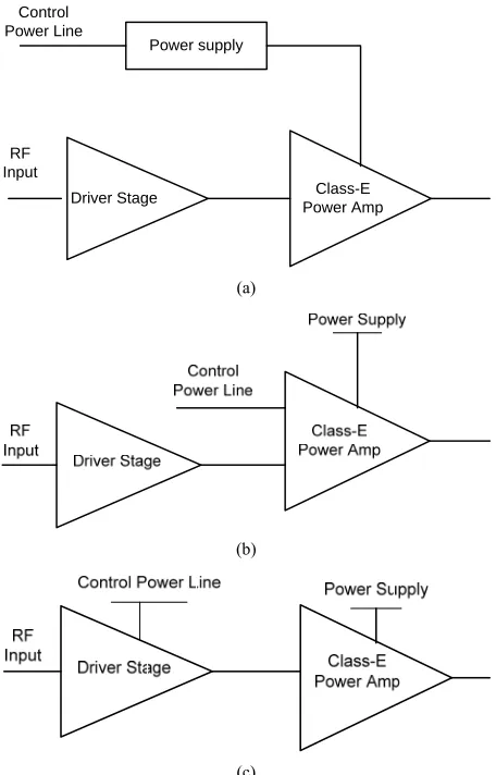
Many power control techniques [4-9] have been car-ried out before. For example, the conventional power con- trol of a switch-mode PA is implemented by adjusting the supply voltage [11]. Figure 1(a) Power control
tech-niques for a constant envelope modulation schemes can be used to improve the efficiency of the PA. For a switch mode PA, the input power is expected to be constant, and therefore a supply voltage power control technique is traditionally employed. High sensitivity to load varia-tions and limited output power control range are main drawbacks of supply voltage power control technique. And also the switch mode power controller is placed in the high power path [6]. Cascode Power Control Tech-nique is another power control techTech-nique that is shown in
Figure 1(b). The power control signal is applied to the
gate of the cascode transistor.
Class-E Power Amp Power supply
Driver Stage Control
Power Line
RF Input
(a)
(b)
(c)
Figure 1. (a) The conventional power control of a switch- mode PA is implemented by adjusting the supply voltage; (b) Cascode Power Control Technique; (c) Block diagram pro- posed power control technique for class E power amplifier
In [12] a two point modulation technique is proposed. The amplitude modulation is implemented by controlling the current of the PA and simultaneously the supply voltage is adjusted in order to improve the efficiency of PA. Low pass delta sigma modulator with a phase modulated clock is used to modulate the envelope which is another approach [12]. Turing on and off an array of cells according to a digital amplitude control signal, is a digital method for amplitude modulation.
The block diagram proposed technique is shown in
Figure 1(c). With this proposed technique, we received
the better PAE characteristic. In this structure, output power controlling is accommodated by driver stage. In Section 2 the technique is described.
This paper is organized as follows. Section 2 describes the basic operation and design implementation of used architecture. Simulation results and analysis are pre- sented in Section 3. Finally, the conclusions are pre- sented in Section 4.
2. Proposed Circuit
2.1. Base Structure
Figure 1(c) shows the schematic diagram of the de-
signed two stage fully-integrated PA. It is a two stage class-E power amplifier. The circuit consists of two stages, a class-E output stage and a driver stage. Figure 2
shows the proposed class-E output stage. Ideally, M1 and M3 act as switch; one-transistor switches on and the other off alternatively in every cycle. The conditions of operation in class-E (hard switching operation and zero- voltage switching condition [8]) allow for a great reduce- tion in power losses, and the tuning of harmonic load impedances is far less sophisticated than in classes rely- ing on tuning of harmonic impedances. The Common Gate transistor is biased so as to be always ON. That keeps the values of on-resistance low, thus limiting the losses and improving efficiency. Traditionally, the self- biased cascode configuration [6] was introduced to opti- mally divide the voltage swing across the Common Source and Common Gate transistors for higher output power and efficiency within the breakdown limits of the device. The common-source (CS) transistor M1 is de- signed to operate as a switch that operates in both, satu- ration and triode region.
The required output power level and the breakdown voltage of the NMOS device set the maximum load im- pedance RL. The power amplifier is designed to deliver output power for output stage. However, to achieve the desired performance, the output stage requires a high peak voltage. Thus a high gain preamplifier must be de- signed to deliver the necessary driver level. The large size output stage transistor implies the need for the pre- ceding stage to drive a huge capacitor. Therefore the first stage of the preamplifier needs to be small to minimize the capacitor seen by the mixer and the final stage of the preamplifier must be large to drive the large capacitor presented by the output stage transistors. In addition, to minimize the capacitive loading an inductor can be used at the gate of the large transistors to resonate its capacitor. An inductor with moderate value has reasonable imped- ance at RF frequency. To maintain the overall efficiency
R1 c1
L1 L4
l2
L3
C4
c2
C3 M2 M4
M3
M1 Vb
Vin
VDD1 VDD
Vbias
Vout +
[image:2.595.59.287.84.440.2] [image:2.595.312.538.597.713.2]
close to that of the output stage, the preamplifier DC current need to be small. For controlling output power, in this work power control line is applied to the gate of the M1 transistor common source stage.
2.2. Relations and Equations
Consider Power amplifier shown in Figure 2. The input
voltage (Vg) is sufficiently low (typically not much greater than the threshold voltage of M1 Transistor), so that M1 is OFF. As Vg is increased, M1 Transistor is ON. Voltage gate of M1 transistor is composed of DC and ac components. DC component is determined by Vbias and amplitude of ac component is determined by preamplifier stage.
1 1sin
1g bias TH
V t V V t V (1)
VTH is threshold voltage of transistor, oscillation frequency and Vbias is bias voltage of Transistor M1. The transistor M1 is off after t2. Also, duty cycle is
1
2 1
1
2 sin TH bias
in
V V
D t t
V
(2)
During the time interval D, transistor is ON. The Equation (2) shows that duty cycle (when the transistor is ON) is changed by the voltage bias. Figure 3 shows duty
cycle versus Vbias. And also, linear dependence of on duty cycle the bias voltage indicating that duty cycle can be achieved by linearly the bias voltage.
As reported in [14], the Equation (3) states output power change with D.
2 2 2 2 DD out V P R
(3)
In this equation, VDD is power supply and R is load
-1 -0.5 0 0.5 1
0.8 1 1.2 1.4 1.6 1.8 2 2.2 2.4x 10
[image:3.595.313.541.104.316.2]-10
Figure 3. Duty cycle versus Vbais (V1 = 2, fin = 2.4 GHz, Vth
= 0.55, Vbias = −1 to 1).
branch network and αand β is expressed by (4) and (5)
sin 2 sin
2
cos 2sin
D
F c X c c
D D
F cos c
(4)
2sin x sin D x
(5)
The θD is the phase duration of the switch on 2π
D D
(6)
And the phase duration of switch–off is
2π 1
F D
(7)
The difference the angle phase θX is expressed by 1 cos tan 2 sin D X D D
(8)
The θC can be expressed by Equation (9) as a function of the phase of switch on θD.
2
c D X
[image:3.595.58.289.523.714.2] (9)
Figure 4 shows output power with respect to duty
cy-cle (D). Output power increases as D. We can conclude that power should be changed with change by Vbias.
3. Post Layout Simulation Result
The power amplifier complete circuit consists of the output stage and the preamplifier shown in Figure 2.
Output stage drive is driven by a class E driver stage. In the proposed design, the finite RF choke technique was used and the maximum drain peak is reduced 2.5 VDD [7]. The width and length of transistor M1 is 4600 and 180
[image:3.595.311.536.544.717.2]m and also the width and length of transistor M2 is 8200 and 350 m, respectively. The spiral on chip L2 (2.6 nH) and C1 (6 pF) and C2 (8 pF) are the interstage matching network. The L1, L3 (5 nH) and L4 (5 nH) are
realized via bond wire inductor. The proposed power amplifier with output power levels in the range of −14 dBm to 23 dBm and with efficiencies ranging from 0% - 38% has been presented. Figure 5 shows transient re-
sponse of voltage gate node transistor M1 versus Vbias. DC voltage of gate M1 transistor increases with increas- ing Vbias. Figure 6 depicts the output power and effi- ciency versus the variation of the supply voltage VDD. By changing the gate voltage of M1 transistor, to the output stage as shown in Figure 2, output power is con-
trollable. Figure 7 shows that proposed technique pro-
vides output power from −14 to 23 dBm whereas; Vbias changes from 0 to 900 mv. As a result, Pout dynamic range is 37 dB. In the Vbias 700 mv, the maximum PAE power amplifier is 38%. Figure 8 shows PAE proposed
power amplifier versus Vbias. The proposed power ampli-
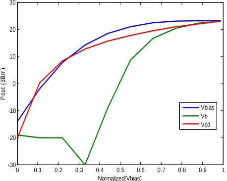
fier has good average power added efficiency with changing Vbias from 0 to 900 mv, PAE changing from 0 to 38% and average, PAE is 27% for all of range control voltage (Vbias). The results in Figure 9 show that the proposed modulated PA is more power efficient than the power supply modulated PA and cascode modulated PA. The proposed PA has good average PAE than other tech- niques. Figure 10 shows the pout versus normalized
control voltage, for changing power supply voltage, voltage gate M2 transistor (cascade transistor) and volt- age gate of M1 transistor. PAE and Pout versus fre- quency for different Vbias is plotted in Figures 11 and 12 respectively. The proposed Power amplifier has 1.2 × 0.6 mm area without pads and bond wire inductors. Figure 13 shows Layout photo of the proposed power amplifier. Table 1 shows the comparison parameters of the pro-
Table 1. Comparison Table of power amplifiers
Reference Frequency (GHz) Technology (micrometer) output power(dBm) Power supply(volt) Peak PAE (%) Dynamic range (dB)
[6] 1.9 0.18 32 3.3 40 20
[13] 1.7 0.25 25 1.5 49 17
[9] 2.2 0.18 18 1.6 35 35
This work 1.8 0.18 23 1.8 38 37
Figure 5. M1 transistor gate node voltage waveforms for different Vbias
Figure 8. Power added efficiency of proposed power am- plifier versus Vbias.
0 0.1 0.2 0.3 0.4 0.5 0.6 0.7 0.8 0.9 1 0
5 10 15 20 25 30 35 40
Normalized (Vbias)
PA
E(
%
)
[image:5.595.58.286.86.213.2]Vbias Vb Vdd
Figure 9. Power Added Efficiency power amplifier versus Vbias (0 to 1 v) and voltage gate of M2 transistor (0 to 1.8 v)
and power supply (0 to 1.8 v) are normalized.
0 0.1 0.2 0.3 0.4 0.5 0.6 0.7 0.8 0.9 1
-30 -20 -10 0 10 20 30
Normalized(Vbias)
Po
u
t (
d
Bm
)
Vbias Vb Vdd
Figure 10. Output power of PA versus Vbias (0 to 1 v) and
voltage gate of M2 transistor (0 to 1.8 v) and power supply (0 to 1.8 v) are normalized.
1.65 1.7 1.75 1.8 1.85 1.9 1.95 2
20 22 24 26 28 30 32 34 36 38
Frequency(GHz)
PA
E
(%
)
[image:5.595.61.286.258.449.2]500mv 600mv 7000mv
Figure 11. Power Added Efficiency power amplifier versus Frequency.
1.65 1.7 1.75 1.8 1.85 1.9 1.95 2
18 19 20 21 22 23 24
Frequency(GHz)
Po
u
t(
d
Bm
)
[image:5.595.311.535.274.434.2]500mv 600mv 700mv
Figure 12. Output power versus frequency.
Figure 13. Layout photo of the class-E PA.
posed PA with the published CMOS PAs.
4. Conclusion
[image:5.595.308.539.462.601.2] [image:5.595.59.288.509.692.2]This power amplifier is capable of delivering 24 dBm output power to a 50 Ω load at 1.8 GHz.
REFERENCES
[1] C. D. Presti, F. Carrara, A. Scuderi, P. M. Asbeck and G. Palmisano, “A 25 dBm Digitally Modulated CMOS Po- wer Amplifier for WCDMA/EDGE/OFDM With Adap-tive Digital Predistortion and Efficient Power Control,”
IEEE Journal of Solid-State Circuits, Vol. 44, No. 7, 2009, pp. 1883-1896.
http://dx.doi.org/10.1109/JSSC.2009.2020226
[2] N. O. Sokal, “Class-E RF Power Amplifiers,” QEX, No. 204, 2001, pp. 9-20.
[3] F. H. Raab, P. Asbeck, S. Cripps, P. B. Kenington, Z. B. Popovich, N. Pethecary, J. F. Sevic and N. O. Sokal, “RF and Microwave Power Amplifier and Transmitter Tech- nologies—Part 2,” High Frequency Electronics, 2003, pp. 39-48.
[4] P. Wagh and P. Midya, “High-Efficiency Switched-Mode RF Power Amplifier,” Proceedings of Midwest Sympo-sium on Circuits and Systems, Vol. 2, 1999, pp. 1044- 1047.
[5] P. Reynaert and M. Steyaert, “A 1.75-GHz Polar Modu-lated CMOS RF Power Amplifier for GSM-EDGE,”
IEEE Journal of Solid-State Circuits, Vol. 40, No. 12, 2005, pp. 2598-2608.
http://dx.doi.org/10.1109/JSSC.2005.857425
[6] Ch. Park, Y. Kim, H. Kim and S. Hong, “A 1.9-GHz CMOS Power Amplifier Using Three-Port Asymmetric Transmission Line Transformer for a Polar Transmitter,”
IEEE Transactions on Microwave Theory and Techniques, Vol. 55, No. 2, 2007, pp. 230-238.
http://dx.doi.org/10.1109/TMTT.2006.889152
[7] C. Yoo and Q. Huang, “A Common-Gate Switched 0.9-W Class-E Power Amplifier with 41% PAE in 0.25-_m CMOS,” IEEE Journal of Solid-State Circuits, Vol. 36, No. 5, 2001, pp. 823-830.
http://dx.doi.org/10.1109/4.918921
[8] T. Sowlati and D. M. W. Leenaerts, “A 2.4 GHz 0.18-_m CMOS Selfbiased Cascode Power Amplifier,” IEEE Jour- nal of Solid-State Circuits, Vol. 38, No. 8, 2003, pp. 1318-1324. http://dx.doi.org/10.1109/JSSC.2003.814417 [9] D. Sira, P. Thomsen and T. Larsen, “Output Power
Con-trol in Class-E Power Amplifiers,” IEEE Microwave and Wireless Components Letters, Vol. 20, No. 4, 2010. http://dx.doi.org/10.1109/LMWC.2010.2042562
[10] T. W. Kwak, M. C. Lee and G. H. Cho, “A 2 W CMOS Hybrid Switching Amplitude Modulator for EDGE Polar Transmitters,” IEEE International Solid-State Circuits Con- ference, San Francisco, 11-15 February 2007, pp 518- 619.
[11] J. N. Kitchen, I. Deligoz, S. Kiaei and B. Bakkaloglu, “Polar SiGe Class E and F Amplifiers Using Switch-Mo- de Supply Modulation,” IEEE Transactions on Micro-wave Theory and Techniques, Vol. 55, No. 5, 2007, pp. 845-856.
http://dx.doi.org/10.1109/TMTT.2007.895407
[12] A. Shameli, A. Safarian, A. Rofougaran, M. Rofougaran and F. De Flaviis, “A Two-Point Modulation Technique for CMOS Power Amplifier in Polar Transmitter Archi-tecture,” IEEE Transactions on Microwave Theory and Techniques, Vol. 56, No. 1, 2008, pp. 31-38.
http://dx.doi.org/10.1109/TMTT.2007.912012
[13] A. Shirvani, D. Su and B. Wooley, “A CMOS RF Power Amplifier with Parallel Amplification for Efficient Power Control,” IEEE Journal of Solid-State Circuits, Vol. 37, No. 6, 2002, pp. 684-693.
http://dx.doi.org/10.1109/JSSC.2002.1004572