International Journal of Emerging Technology and Advanced Engineering
Website: www.ijetae.com (ISSN 2250-2459,ISO 9001:2008 Certified Journal, Volume 4, Issue 7, July 2014)
518
Efficient Design of Reversible Multiplexers with Low Quantum
Cost and Power Consumption
Ashima Malhotra
1, Charanjit Singh
2, Amandeep Singh
31Student, 2,3Assistant Professor, Department of Electronics and Communication Engineering, Punjabi University, Patiala
Abstract- Multiplexing is the generic term used to designate the operation of sending one or more analogue or digital signals over a common transmission line at dissimilar times or speeds and as such, the scheme we use to do just that is called a Multiplexer. In digital electronics, multiplexers are similarly known as data selectors as they can “select” each input line, are made from individual Analogue Switches encased in a single IC package as conflicting to the “mechanical” type selectors such as standard conservative switches and relays. In today era, reversibility has become essential part of digital world to make digital circuits more efficient. In this paper, we have proposed a new method to reduce quantum cost and power for various multiplexers. The results are simulated in Xilinx by using VHDL language.
Keywords- FRG Gate , MFRG Gate , Multiplexer , Power Consumption , Quantum Cost.
I. INTRODUCTION
Reversible logic performs all operations in an invertible manner that marks a promising new direction. As compared with traditional logic, all computations can be reverted (i.e. the inputs can be obtained from the outputs and vice versa) by using reversible logic. This reversibility plays significant role for emerging technologies that may replace or at least enhance the traditional computer chip efficiency. Power dissipation and heat generation is a serious problem for today‟s computer chips. The non-ideal behavior of transistors and some other materials becomes primary cause for the power dissipation. A more fundamental reason for power dissipation arises from the observations made by Landauer in 1961. Landauer proved that using traditional (irreversible) logic gates always lead to energy
dissipation. More precisely, exactly
kT
log
2 Joule of energy is dissipated for each “lost” bit of information during the irreversible operation (wherek
is the Boltzmann constant andT
is the temperature). [1][9]Quantum Computation and Quantum Information can be accomplished using Quantum mechanical systems and is the study of the information processing tasks. Quantum mechanics is a mathematical schema or set of rules for the construction of physical theories.
Quantum computation directed us to think physically about computation, and this approach turnouts many new and exciting capabilities for information processing and communication. [7]
To implement reversible computation, estimate its cost, and to judge its limits, it is formalized it in terms of gate-level circuits. Reversible computing will also lead to improvement in power efficiency. Power efficiency will fundamentally affect the speed of circuits such as nanocircuits— and therefore the speed of most computing applications. [9]
A. Quantum Cost
Quantum Cost of the circuit is considered by knowing the number of simple reversible gates (gates of which rate is previously identified) needed to realize the circuit.
B. Garbage Output
The output of the reversible gate that is not used as a main output or as input to other gates is called the garbage output. In little the unexploited output of a reversible gate (or circuit) is the garbage output (s). These garbage outputs are required in the circuit to retain the reversibility concept.
[9]
C. Organization of the work
This section describes the organization of the paper. Section I includes the introduction of reversibility. Section II shows the work done by the various researchers in the field of reversibility.. Section III describes the concept of reversible logic gates . Section IV includes the proposed work. Section V includes results and discussions Section VI includes conclusion with future scope. References are shown in next section.
II. LITERATURE SURVEY
International Journal of Emerging Technology and Advanced Engineering
Website: www.ijetae.com (ISSN 2250-2459,ISO 9001:2008 Certified Journal, Volume 4, Issue 7, July 2014)
519
The SPICE simulation shows that the proposed dynamic ripple carry adders are at least two times faster than the conventional static ripple carry adder. T. Himanshu et al[7] described that the reversible logic has emerged as a promising technology having its applications in low power CMOS, quantum computing, nanotechnology, and optical computing. The classical set of gates such as AND, OR, and EXOR are not reversible. This work proposed a new
reversible gate called “TSG” gate. The proposed gate was used to design efficient adder units.
From above literature survey, it has been concluded that reversibility is essential for new technologies in terms of power efficiency. This can be done if the quantum cost and garbage output value of the digital circuits should be reduced which can only be possible by using reversible logic gates.
III. REVERSIBLE LOGIC GATES [7][10]
A. Peres Gate (PG)
The (Peres, 1985) is designated as follows: Input vector and output vector
[image:2.612.337.584.135.206.2]. Block diagram of Peres is showed in Fig. 1. Peres gate is the combination of Feynman gate and Toffoli gate and this can contrivance operations like AND EX-OR. In this projected design PG gate is used for performing AND operation. The quantum cost of Peres gate is 4.
Figure 1: Peres gate
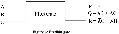
B. Fredkin Gate (FRG)
Input and output vectors for 3×3 FRG (Fredkin and Toffoli, 1982) is well-defined as follows: and ̅ ̅ FRG gate is showed in Fig. 2 and it is used in to hypothesis Multiplexers circuits. This gate is used in the planned designs for execution both AND and OR operation. This AND-OR output is attained at output R. The quantum cost of Peres gate is 5.
Figure 2: Fredkin gate
C. Modified Fredkin Gate (MFRG)
[image:2.612.330.559.329.421.2]Input and output vectors for 3×3 FRG (Fredkin and Toffoli, 1982) is well-defined as follows: and ̅ ̅ ̅ MFRG gate is showed in Fig. 3 and it is used in to hypothesis in Multiplexers circuits. This gate is used in the planned designs for execution both AND and OR operation. This AND-OR output is attained at output R. The quantum cost of Peres gate is 4.
Figure 3: Modified Fredkin gate
D. MTSG Gate
Modified TSG (MTSG) gate is a 4×4 reversible gate with following input and output vectors,
and and
. This MTSG gate in Fig. 4 can be recycled to recognize a full adder by providing constant „0‟ at the input D. Quantum cost of changeable MTSG gate is 6 which is lower than 13 of TSG gate. This gate is used in the enterprise so as to produce the sum, carry and the spread output of the inputs.
[image:2.612.62.283.465.541.2]International Journal of Emerging Technology and Advanced Engineering
Website: www.ijetae.com (ISSN 2250-2459,ISO 9001:2008 Certified Journal, Volume 4, Issue 7, July 2014)
520
E. MHNG Gate
[image:3.612.330.585.139.375.2]MHNG gate is a 4x4 reversible gate with following input and output vectors, Iv = (A, B, C, D) and Ov = (P = A, Q = D, R = A B C, S = (A B).C AB D). The MHNG gate is shown in Fig .5, where each output is annotated with the corresponding logic expression. One of the prominent functionalities of the MHNG gate is that it can work singly as a reversible full adder unit.
Figure 5: MHNG Gate
IV. PROPOSED WORK
A. 2:1 Multiplexer
Fig. 6 shows the proposed architecture for 2:1 MUX using MFRG gate.
Figure 6: 2:1 MUX using MFRG gate
B. 4:1 Multiplexer
Fig. 7 shows the proposed architecture for 4:1 MUX using MFRG gates.
Figure 7: 4:1 MUX using MFRG gates
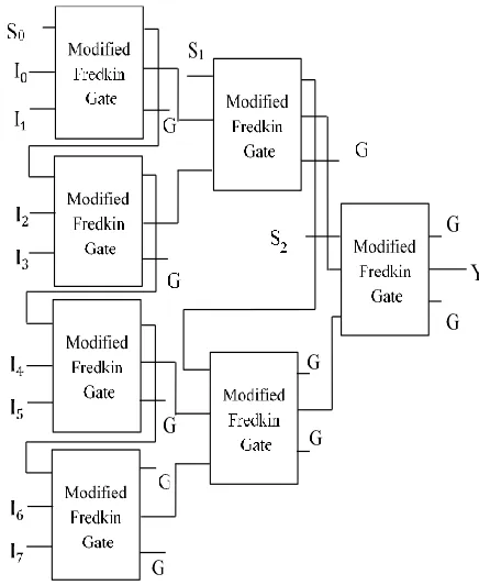
C. 8:1 Multiplexer
Fig. 8 shows the proposed architecture for 8:1 MUX using MFRG gate.
[image:3.612.53.240.241.374.2] [image:3.612.335.553.440.706.2]International Journal of Emerging Technology and Advanced Engineering
Website: www.ijetae.com (ISSN 2250-2459,ISO 9001:2008 Certified Journal, Volume 4, Issue 7, July 2014)
521
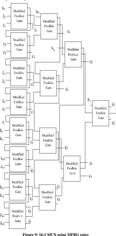
D. 16:1 Multiplexer
[image:4.612.52.569.134.656.2]Fig. 9 shows the proposed architecture for 16:1 MUX using MFRG gate.
Figure 9: 16:1 MUX using MFRG gates
V. RESULTS AND DISCUSSIONS
Table I
Comparison of proposed work with existing work
Quantum Cost
Power (W) 2:1
MUX
Using FRG Gates 5 2.070
Using MFRG Gates
4 1.701
4:1 MUX
Using FRG Gates 15 1.898
Using MFRG Gates
12 1.754
8:1 MUX
Using FRG Gates 35 2.017
Using MFRG Gates
28 1.754
16:1 MUX
Using FRG Gates 75 2.013
Using MFRG Gates
60 1.834
[image:4.612.320.568.164.629.2] [image:4.612.54.292.172.654.2]International Journal of Emerging Technology and Advanced Engineering
Website: www.ijetae.com (ISSN 2250-2459,ISO 9001:2008 Certified Journal, Volume 4, Issue 7, July 2014)
[image:5.612.48.295.123.418.2]522
Figure 11: Graphs showing power consumption for 4:1 Multiplexer [image:5.612.321.570.131.409.2]using reversible MFRG gates
Figure 12: Graphs showing power consumption for 8:1 Multiplexer using reversible MFRG gates
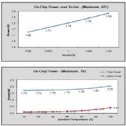
Figure 13: Graphs showing power consumption for 16:1 Multiplexer using reversible MFRG gates
The proposed reversible multiplexers are more efficient than the existing circuits presented in [10]. Evaluation of proposed circuit can be comprehended easily with the help of the comparative results in Table 1. Therefore, the proposed multiplexers are better than the existing circuits in terms of complexity. One of the other major constrains in designing a reversible logic circuit is less quantum cost.
VI. CONCLUSION
In this paper, we presented reversible multiplexers using MFRG gates. Table 1 demonstrates that the proposed reversible multiplexers are better than the existing designs in terms of hardware complexity and quantum cost. Our proposed reversible multiplexers can be applied to the design of complex systems in nanotechnology.
A. Future Scope
This paper opens up some possible research directions which are described below:
The demultiplexers can be optimized using various reversible logic gates having low power and quantum cost.
[image:5.612.48.299.448.700.2]International Journal of Emerging Technology and Advanced Engineering
Website: www.ijetae.com (ISSN 2250-2459,ISO 9001:2008 Certified Journal, Volume 4, Issue 7, July 2014)
523
REFERENCES[1] R. Landauer, “Irreversibility and Heat Generation in the
Computational Process”, IBM Journal of Research and Development, 5, 196 , pp. 183-191.
[2] R. H. M and T. Kaylani, "VLSI design of a quaternary carry ripple adder." System Theory," in Proceedings., Twenty-First Southeastern Symposium on. IEEE, 1989.
[3] C. C. Nez and E. A. Vittoz, Digital Integrated Circuits: A design Perspective. “Charge-Based MOS Transistor Modeling," 1996. [4] M. Vratonjic, B. R. Zeiden and V. G. Oklobdzija, "Low-and Ultra
Low-Power Arithmetic Units: Design and Comparison," in Proceedings of the IEEE International Conference on Computer Design: VLSI in computers and processors, 2005.
[5] Md. M. H Azad Khan, “Design of Full-adder With Reversible Gates”, International Conference on Computer and Information Technology, Dhaka, Bangladesh, 2002, pp. 515-519.
[6] H. Thapliyal and M. Srinivas, "Novel design and reversible logic synthesis of multiplexer based full adder and multipliers," in Circuits and Systems, 2005. 48th Midwest Symposium on, 2005.
[7] M. Khan, "Reversible Realization of Quaternary Decoder,
Multiplexer, and Demultiplexer Circuits," in Multiple Valued Logic, 2008. ISMVL 2008. 38th International Symposium on, 2008. [8] G. Maity, T. Chattopadhyay, J. Roy and S. Maity, "All-optical
reversible multiplexer," in Computers and Devices for
Communication, 2009. CODEC 2009. 4th International Conference on, 2009.
[9] Robert Wille, Rolf Drechsler, Towards a Design Flow for Reversible Logic, Springer, 2010.