Power Efficient Fir Filter Design
PG scholar, VLSI design,
P.A College of Engineering and Technology,
Abstract: Finite Impulse Response (FIR) digital filter is basic component in communication systems and in many digital signal processing (DSP). FIR filter is broadly used in portable application with small area and low power.
signal decision logic and amplitude detection logic we can reduce the power of FIR filter. In FIR filter extensive variations
data and in coefficient. The filter order is dynamically changed in accordance with amplitude of both filter input data and f coefficients. The power of the proposed FIR filter is reduced by 5mW from previous fir filter.
KeyWords: Finite impulse response (FIR), approximate filtering, low power filter, reconfigurable design
I.INTRODUCTION
Demand for the low power digital signal processing (DSP) is increasing day by day. Finite impulse response (FIR) is the major operation used in the DSP. A general FIR filter of order N can be expressed as equation (1):
( ) = ∑ ( − )…………(1)
Where N denotes the length of FIR filter,
coefficient, and x( n –i ) is the input data at the time instant
–i. In large DSP application FIR filter with considerably large number of taps are required. Reducing the area and power ingestion is the main intention of many previous papers while maintaining the fixed filter order[1]–[3]. In those papers add and shift operations are applied to the FIR filter structure to minimize the number of addition and subtraction.
The main drawback come across for those approaches are that once the filter architecture is decided, the coeff cannot be changed so that these techniques are not relevant FIR filter with programmable coefficients. For the design of low power digital filter [5], [6], approximate signal processing [4] is used. [6] Shows that the energy quality characteristics FIR filter can be improved by sorting both the data samples and filter coefficients before the convolution operation. Area efficient FIR filter [base] design in achieved with the help of faithfully rounded truncated MCMA.
Real time sorting of all incoming samples are very difficult. Reconfigurable FIR filter architectures [7]-[9] are used for low power implementations or to recognize several frequency responses by means of a single filter [10].
Power Efficient Fir Filter Design
Ranjini.C, Thiruvenkadam.S
PG scholar, VLSI design,HOD,IT Department, College of Engineering and Technology,
Tamilnadu, India
Finite Impulse Response (FIR) digital filter is basic component in communication systems and in many digital signal filter is broadly used in portable application with small area and low power. In this work by using multiple control signal decision logic and amplitude detection logic we can reduce the power of FIR filter. In FIR filter extensive variations
data and in coefficient. The filter order is dynamically changed in accordance with amplitude of both filter input data and f The power of the proposed FIR filter is reduced by 5mW from previous fir filter.
response (FIR), approximate filtering, low power filter, reconfigurable design
Demand for the low power digital signal processing (DSP) is increasing day by day. Finite impulse response (FIR) used in the DSP. A general FIR filter of
…………(1)
denotes the ith is the input data at the time instant n
. In large DSP application FIR filter with considerably large number of taps are required. Reducing the area and power ingestion is the main intention of many previous papers while [3]. In those papers add and shift operations are applied to the FIR filter structure to minimize the number of addition and subtraction.
The main drawback come across for those approaches are that once the filter architecture is decided, the coefficients cannot be changed so that these techniques are not relevant FIR filter with programmable coefficients. For the design of low power digital filter [5], [6], approximate signal processing [4] is used. [6] Shows that the energy quality characteristics of FIR filter can be improved by sorting both the data samples and filter coefficients before the convolution operation. Area efficient FIR filter [base] design in achieved with the help of
oming samples are very difficult. [9] are used for low power implementations or to recognize several frequency
A area and power efficient FIR filter architecture is d
where the filter order can be changed with respect to the amplitude of both filter coefficient and the inputs. Area of FIR filter is reduce using the concept of faithfully rounded truncated MCMA and the power can be reduce by cancelling unwanted multiplication operation.
II. EXISTING FIR FILTER ARCHITECTURE
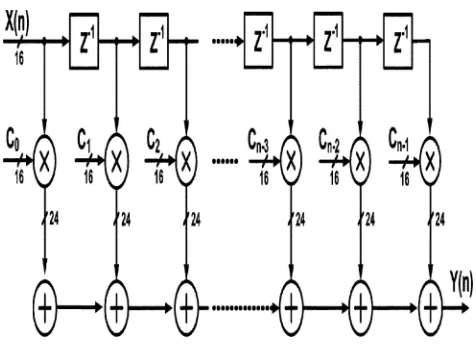
The direct form of FIR filter is adopting for this project. The direct form of a FIR filter is as shown in fig.1.where all
[image:2.612.314.552.440.617.2]products in bi × x [n –i] are summed up with MCMA module.
Fig -1: Architecture of Direct form FIR filter.
The existing method will efficiently collect all the partial products (PP) into a single PPB matrix with carry addition. It is more efficient than accumulating individual
Power Efficient Fir Filter Design
Finite Impulse Response (FIR) digital filter is basic component in communication systems and in many digital signal In this work by using multiple control signal decision logic and amplitude detection logic we can reduce the power of FIR filter. In FIR filter extensive variations occur in input data and in coefficient. The filter order is dynamically changed in accordance with amplitude of both filter input data and filter
A area and power efficient FIR filter architecture is designed, where the filter order can be changed with respect to the amplitude of both filter coefficient and the inputs. Area of FIR filter is reduce using the concept of faithfully rounded truncated MCMA and the power can be reduce by cancelling
II. EXISTING FIR FILTER ARCHITECTURE
The direct form of FIR filter is adopting for this project. The direct form of a FIR filter is as shown in fig.1.where all are summed up with MCMA module.
1: Architecture of Direct form FIR filter.
I N T E R N A T I O N A L J O U R N
AN D E N G IN E E
multiplication for each product. This operation will reduce the matrix height to two, followed by a final carry propagation adder.
Faithfully rounding and truncating method of operation is implemented in the FIR filter to reduce the number of arithmetic operation. The total error in arithmetic operation introduced in this method is not larger than one ulp. The most recent truncated multiplier design is as shown in the fig.2.
Fig -2: improved version of truncated multiplier designs using the approach in [ 12].
In the improved version of truncated multiplier designed using the approach [13] can delete more PPBs which leads to the reduction in area cost. This multiplier made a single row of PPBs undeletable and also the elimination of the PPB consists of deletion and rounding. By using t
version of truncation design an architecture of MCMA with truncation (MCMAT) which removes the unnecessary PPBs as shown in fig 3.In fig 3 the L-shaped block with white circles represents the undeletable PPBs. Gray color circles represents the deletion of PPBs. The crossed circles represent the rounding of resultant bits after PP compression. All the offset and bias constants required including the sign bit modifications are represented in the last row of PPB matrix.
III. PROPOSED FIR FILTER STRUCTURE
Fig 1 shows the direct form FIR filtering operation performs the convolution, the weighted summations of input sequences. Low pass, high pass and band pass filters are using
N A L F O R R E S E A R C H I N A P P L I E
E R I N G T E C H N O L O GY (I J R A S E T
his operation will reduce the al carry propagation
Faithfully rounding and truncating method of operation is implemented in the FIR filter to reduce the number of metic operation introduced in this method is not larger than one ulp. The most recent truncated multiplier design is as shown in the fig.2.
2: improved version of truncated multiplier designs
of truncated multiplier designed using the approach [13] can delete more PPBs which leads to the reduction in area cost. This multiplier made a single row of PPBs undeletable and also the elimination of the PPB consists of deletion and rounding. By using the improved version of truncation design an architecture of MCMA with truncation (MCMAT) which removes the unnecessary PPBs shaped block with white circles represents the undeletable PPBs. Gray color circles deletion of PPBs. The crossed circles represent the rounding of resultant bits after PP compression. All the offset and bias constants required including the sign bit modifications are represented in the last row of PPB matrix.
TRUCTURE
1 shows the direct form FIR filtering operation performs the convolution, the weighted summations of input sequences. Low pass, high pass and band pass filters are using
the convolution operation to realize frequency selective application. The FIR filter power consumption and its amount of computation is directly proportional to its order. So that we can achieve significant power saving by reducing the filter order by turning off some of the multiplier. The degradation of filter performance should be considered when we change the filter taps.
Coefficients of a typical 25-tap low pass FIR filter is shown in fig 4. The central coefficient
in 25- tap filter and the amplitude of the coefficient decreases
[image:3.612.85.537.222.426.2]askbecomes more distant from the centre tap.
Fig -3: Overall FIR filter architecture using multiple constant multipliers/accumulators with faithfully rounded truncation (MCMAT).
Fig -4: Amplitude of the 25-tapequi-ripplefiltercoe
E D S C I E N C E
T)
the convolution operation to realize frequency selective e FIR filter power consumption and its amount of computation is directly proportional to its order. So that we can achieve significant power saving by reducing the filter order by turning off some of the multiplier. The degradation hould be considered when we change
tap low pass FIR filter is shown in fig 4. The central coefficient c12 has the largest value
tap filter and the amplitude of the coefficient decreases distant from the centre tap.
3: Overall FIR filter architecture using multiple constant multipliers/accumulators with faithfully rounded truncation
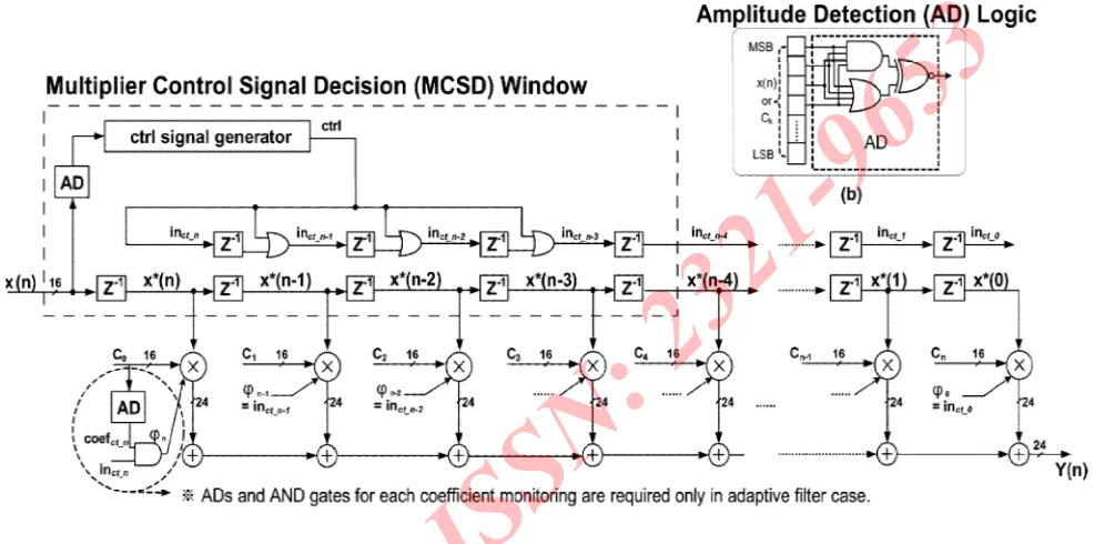
[image:3.612.352.551.484.666.2]The FIR inputs x(n) are multiplied with the coefficients therefore the amplitude of the inputs are also changes. If the amplitudes of both the coefficient and data input of a FIR filter are small then the multiplication of those two numbers are proportionately small. Thus we can turn off the corresponding multiplier has negligible effect on the filter performance.
Fig -5: a) Proposed reconfigurable FIR filter architecture.(b)Amplitude detection logic (AD).
Generally in the fixed width FIR filter full operand bit width of the multiplier is not used. When the bit
input and the filter coefficient are 16, the multiplier generates 32 bit outputs. By considering the circuit area of following adder, the LSB of the multiplier outputs are truncated or rounded off, which incurs quantization error. For example in fig 1, we have used 24 bits. When we turn off the multiplier in the FIR filter, if we can carefully select the input and coefficient amplitudes such that the multiplication of those two numbers are as small as the quantization erro performance degradation can be made negligible.
Considering the threshold of the input is coefficient is cth. We can turn off the multiplier for
the multiplication operation in FIR filter by considering the threshold. If the threshold of the x(n) andckare lesser than its
threshold value, the corresponding multiplier can turn off. When we determine xth and cth, the trade-off between filter
are multiplied with the coefficients therefore the amplitude of the inputs are also changes. If the amplitudes of both the coefficient and data input of a FIR filter are small then the multiplication of those two numbers can turn off the corresponding multiplier has negligible effect on the filter
DSP application are widely using the two’s compliment
data format, if one or both of the multiplier input has negative value, multiplication of two small values giv
switching activities, which is due to the series of 1’s in the
MSB part. Power saving can be achieved by cancelling the multiplication of two small numbers with negligible degradation in filter performance.
a) Proposed reconfigurable FIR filter architecture.(b)Amplitude detection logic (AD).
Generally in the fixed width FIR filter full operand bit-width of the multiplier is not used. When the bit-bit-width of filter input and the filter coefficient are 16, the multiplier generates By considering the circuit area of following the LSB of the multiplier outputs are truncated or rounded off, which incurs quantization error. For example in f the multiplier in , if we can carefully select the input and such that the multiplication of those o numbers are as small as the quantization error, filter
gligible.
Considering the threshold of the input is xth and the
. We can turn off the multiplier for cancelling the multiplication operation in FIR filter by considering the are lesser than its threshold value, the corresponding multiplier can turn off. f between filter
performance and power savings should be carefully considered.
IV.PROPOSED ARCHITECTURE
The architecture of a proposed FIR filter is shown in fig 5(a). To scrutinize the amplitude of data input
the coefficient ck, an amplitude detector (AD), in fig 5(b) is
used. If the amplitude of the one or both multiplier input signals are smaller than the threshold then we can cancel the corresponding multiplication operation. The output of
is set to 1 when the absolute value of
input threshold xth. The design of AD is dependent on the
input threshold xth, where the fan-in’s of AND and OR gate
are decided by xth. If xth and c
adaptively due to designer’s considerations,
implemented using a simple comparator.
DSP application are widely using the two’s compliment
data format, if one or both of the multiplier input has negative value, multiplication of two small values gives rise to large
switching activities, which is due to the series of 1’s in the
MSB part. Power saving can be achieved by cancelling the multiplication of two small numbers with negligible
a) Proposed reconfigurable FIR filter architecture.(b)Amplitude detection logic (AD).
vings should be carefully
IV.PROPOSED ARCHITECTURE
The architecture of a proposed FIR filter is shown in fig 5(a). To scrutinize the amplitude of data input x(n )and also an amplitude detector (AD), in fig 5(b) is used. If the amplitude of the one or both multiplier input signals are smaller than the threshold then we can cancel the corresponding multiplication operation. The output of the AD is smaller than the . The design of AD is dependent on the
in’s of AND and OR gate cth have to be changed
[image:4.612.66.559.187.432.2]I N T E R N A T I O N A L J O U R N
AN D E N G IN E E
Switching activity on the internal node capacitance is a main factor which affects the dynamic power consumption of CMOS logic gate. In this proposed reconfigurable FIR filter, we can turn off the multiplier according to the amplitude of each input. If the amplitude of the input x(n) rapidly changes for every cycle, the multiplier will turn on and off continuously, which produces continuous switching activities.
To control this switching problem we are using
control signal decision (MCSD) window in fig 5(a). MCSD
generate control signal ctrl, which counts the number of input
samples smaller than xth are counted and multipliers are turned
off only when m consecutive input samples are smaller than
xth. In the fig 5(a) mdenotes the size of MCSD. The detailed
diagram of ctrl signal generator design is as shown in fig 6. If an input signal smaller than xthcomes in then the output of the
AD is set to “1”, then the counter is counting up.
Only the first gate of the multiplier is modified and once
the is set to “1”, thereis no switching activity in
nodes and multiplier output is set to “0”. The area overhead
for the proposed reconfigurable filter are flip
signals, AD and ctrl signal generator inside MCSD and the modified gates in fig 7 for turning off multiplier. Those overheads can be implemented using simple logic
single AD is needed for input monitoring
in Fig. 3(a). Consequently, the overall circuit implementing reconfigurable filter is as small multiplier.
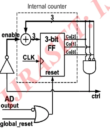
Fig -6: Schematic of ctrl signal generator. Internal counter
sets ctrlsignal to “1” when all input samples inside MCSD are
smaller than xth.
N A L F O R R E S E A R C H I N A P P L I E
E R I N G T E C H N O L O GY (I J R A S E T
Switching activity on the internal node capacitance is a main factor which affects the dynamic power consumption of CMOS logic gate. In this proposed reconfigurable FIR filter, according to the amplitude of rapidly changes for every cycle, the multiplier will turn on and off continuously, which produces continuous switching activities.
To control this switching problem we are using multiplier control signal decision (MCSD) window in fig 5(a). MCSD , which counts the number of input are counted and multipliers are turned off only when m consecutive input samples are smaller than denotes the size of MCSD. The detailed signal generator design is as shown in fig 6. If comes in then the output of the
AD is set to “1”, then the counter is counting up.
gate of the multiplier is modified and once in the following
“0”. The area overhead
for the proposed reconfigurable filter are flip-flops for inct-n
signal generator inside MCSD and the modified gates in fig 7 for turning off multiplier. Those
simple logic gates, and a monitoring as specified circuit overhead for small as a single
signal generator. Internal counter
signal to “1” when all input samples inside MCSD are
The ctrl generator changes to “1”after the counter reaches
m which shows that m successive small inputs are observed and multipliers are set to turn off. To decide the multiplier operation by monitoring the value of c
bit inct-n in fig 5 is added. The additional bit is controlled by ctrland also the inct-naccompanies the data all the way in the
subsequent flipflops to shows that the input sample and the coefficients are smaller than xthand cth
signal is fixed inside the MCSD; it does not change outside the MCSD and hold the amplitude information of the input signal. For the synchronization process between x
n, add a delay component infront of the first strap in fig 5(
since once clock latency is needed due to the counter in MCSD.
[image:5.612.316.550.288.632.2]In case of the adaptive filter more ADs are needed for monitoring the amplitudes of each coefficient as shown in fig 5(a). However, in the FIR filter with fixed or programmable coefficients, since we know the amplitude of coefficients ahead, extra AD modules for coefficient monitoring are not needed.
Fig 7. Modified gate schematic to turn o
After comparing the input and coefficient are smaller than
xth and cth, respectively, the multiplier is turned off by setting
E D S C I E N C E
T)
generator changes to “1”after the counter reaches
m which shows that m successive small inputs are observed and multipliers are set to turn off. To decide the multiplier operation by monitoring the value of cthand xth, one additional
is added. The additional bit is controlled by accompanies the data all the way in the subsequent flipflops to shows that the input sample and the
threspectively. The inct-n
side the MCSD; it does not change outside the MCSD and hold the amplitude information of the input signal. For the synchronization process between x*(n) and in
ct-, add a delay component infront of the first strap in fig 5(a) since once clock latency is needed due to the counter in
In case of the adaptive filter more ADs are needed for monitoring the amplitudes of each coefficient as shown in fig However, in the FIR filter with fixed or programmable since we know the amplitude of coefficients ahead, extra AD modules for coefficient monitoring are not
turn off multiplier
[image:5.612.101.291.418.640.2]Page 148
the output signal to “1”. By using the simple technique
discussed [11] in fig 7, the multiplier can be turned off easily
and the output is enforced to “0”. Fig 7 shows, if the control
signal is “1” then the PMOS turns off and NMOS turns
off, the gate output is enforced to “0” irrespective of the input.
If the value is “0” then the gate will functions like a normal gate.
IV. SIMULATION RESULTS AND COMPARISON
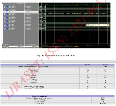
Simulation result of FIR filter by using the two software Xilinx ISE 8.1 and Modelsim 6.3f is given below. The simulated waveform output of FIR filter is as shown below in fig 8. The simulation results are taken by using modelsim 6.3f version software. We generate a output for four tap FIR filter
[image:6.612.82.550.207.634.2]with clk input. The coefficient values are fixed.
Fig .-8: Simulation Result of FIR filter
I N T E R N A T I O N A L J O U R N A L F O R R E S E A R C H I N A P P L I E D S C I E N C E
AN D E N G I N E E R I N G T E C H N O L O G Y (I J R A S E T)
Page 149
The power usage of the proposed FIR filter is as shown below in fig 9. The power consumption value can be found by using the Xilinx ISE 8.1 software. Power usage of this proposed FIR filter is 103mW and this is comparatively less than the power usage of previous FIR filter. And also the delay also has been reduced from 2.636 ns to 1.568 ns.
COMPARISON By using Existing method By using proposed work
POWER 108mW 2.636ns
DELAY TIME 103mW 1.568
V.CONCLUSION
In this paper, we tend to propose less power reconfigurable FIR filter design to permit economical trade-off between the filter performance and computation energy. Within the projected reconfigurable filter, the input data measures are monitored and therefore the multipliers within the filter turned off once each the coefficients and inputs square measure sufficiently small to mitigate the result on the filter output. Therefore, the projected reconfigurable filter dynamically changes the filter order to attain important power savings with minor degradation in performance. Power savings and filter performance degradation square measure diagrammatical as robust functions of MCSD window size, the input and coefficient thresholds, and input signal characteristics. The projected theme achieves power savings up to 41.9% with but around 5.34% of space overhead with terribly sleek degradation within the filter output. The projected approach may be applicable to alternative areas of signal process, wherever a correct trade-off between power savings and performance degradation ought to be rigorously thought-about. the concept bestowed during this paper will assist within the style of FIR filters and its implementation for low power applications.
REFERENCES
[1] H. Samueli, “An improved search algorithm for the design of multiplierless FIR filter with powers-of-two
coefficients,” IEEE Trans. Circuits Syst., vol. 36, no. 7, pp.
1044–1047, Jul. 1989.
[2] R. I. Hartley, “Subexpression sharing in filters using
canonical signed digit multipliers,” IEEE Trans. Circuits
Syst. II, Analog Digit. Signal Process., vol. 43, no. 10, pp. 677–688, Oct. 1996.
[3] O. Gustafsson, “A difference based adder graph heuristic for multiple constant multiplication problems,” in
Proc. IEEE Int. Symp. Circuits Syst., 2007, pp. 1097–1100.
[4] S. H. Nawab, A. V. Oppenheim, A. P. Chandrakasan, J.
M. Winograd, and J. T. Ludwig, “Approximate signal processing,” J. VLSI Signal Process., vol. 15, no. 1–2, pp. 177–200, Jan. 1997.
[5] J. Ludwig, H. Nawab, and A. P. Chandrakasan, “Low
power digital filtering using approximate processing,”
IEEE J. Solid-State Circuits, vol. 31, no. 3, pp. 395–400, Mar. 1996.
[6] A. Sinha, A. Wang, and A. P. Chandrakasan, “Energy scalable system design,” IEEE Trans. Very Large Scale Integr. Syst., vol. 10, no. 2, pp. 135–145, Apr. 2002.
[7] K.-H. Chen and T.-D. Chiueh, “A low-power
digit-based reconfigurable FIR filter,” IEEE Trans. Circuits Syst.
II, Exp. Briefs, vol. 53, no. 8, pp. 617–621, Dec. 2006.
[8] R.Mahesh and A.P.Vinod, “New reconfigurable
architectures for implementing filters with low
complexity,” IEEE Trans. Comput.-Aided Des. Integr. Circuits Syst., vol. 29, no. 2, pp. 275–288, Feb. 2010.
[9] Z. Yu, M.-L. Yu, K. Azadet, and A. N. Wilson, Jr, “A
low power FIR filter design technique using dynamic
reduced signal representation,” in Proc. Int. Symp. VLSI
Tech., Syst., Appl., 2001, pp. 113–116.
[10] R. Mahesh and A. P. Vinod, “Coefficient decimation
approach for realizing reconfigurable finite impulse response filters,” in Proc. IEEE Int. Symp. Circuits Syst., 2008, pp. 81–84.
[11] J. Park and K. Roy, “A low complexity reconfigurable
DCT architecture to trade off image quality for power
consumption,” J. Signal Process. Syst., vol. 53, no. 3, pp.
399–410, Dec. 2008.
[12] J. G. Proakis, Digital Communications, 3rd ed. New York: McGraw-Hill, 1995.
[13] Shen-Fu Hsiao, Jun-Hong Zhang Jian, and Ming-Chih
Chen ,”Low-Cost FIR Filter Designs Based on Faithfully
Page 150 Multiplication/Accumulation” IEEE Trans. Circuits Syst.
II,: Exp.Brief, vol. 60, no. 5,may 2013.
[14] H.-J. Ko and S.-F. Hsiao, “Design and application of faithfully rounded and truncated multipliers with combined
deletion, reduction, truncation, and rounding,” IEEE Trans.
Circuits Syst. II, Exp. Briefs, vol. 58, no. 5, pp. 304–308, May 2011.
BIOGRAPHIES
Ranjini.c received the B.E. and. degrees in electronics and communication engineering from Anna University, Chennai, in 2012 and doing the M.E degree in VLSI Design in the Anna University ,Chennai. Her research interest includes low power circuit and system design for digital signal processing and digital communications.
![Fig -2: improved version of truncated multiplier designs using the approach in [ 12].2: improved version of truncated multiplier designs](https://thumb-us.123doks.com/thumbv2/123dok_us/8588229.863059/3.612.352.551.484.666/improved-version-truncated-multiplier-approach-improved-truncated-multiplier.webp)