Technology (IJRASET)
Graphical User Interfacing of Test Stimulus
Generation for Sigma Delta ADC Built in Self-Test
Shiv Ashish Agrahari#1, Anil Kumar Sahu#2 #
SSTC, Bhilai, India
Abstract— In this paper, a test stimulus generator with graphical user interfacing is proposed which can be realize on chip
with high area utilization. The generated test stimulus can be used to find out the static (offset error, gain error, integral nonlinearity error and differential nonlinearity error) and dynamic (signal to noise ratio, effective no. of bits and signal to noise and distortion ratio) parameter of the sigma delta analog to digital converter. It is possible to fabricate on chip generator so that we can use this generator.
Keywords— Graphical user interface, test stimulus generator, sigma delta modulator, analog to digital converter, built in
self-test, on chip testing, sigma delta ADC
I. INTRODUCTION
System-on-a-chip (SOC) design may contain digital, memory, analog and mixed-signal cores. Testing for an SOC chip is a challenging task, especially for its analog and mixed-signal cores.
The most commonly used mixed signal devices are analog-to-digital (A/D) converters and digital-to-analog (D/A) converters. The conventional test methods for A/D and D/A converters mainly focus on functional tests, which are both expensive and time-consuming [1], [2]. To resolve the problem, one promising strategy is the built-in self-test approach in which both stimulus generation and response measurement are performed on the chip [3]. In this paper, we focus on developing efficient test stimulus generator for built in self-test schemes for testing A/D converters.
II. LITERATURE REVIEW
In [4], [5], [6], described a memory based pattern generator. Where bit streams are already present in RAM type of memory. Data is stored in memory at the time of fabrication or with the help of storing the output data of design under test (analog to digital converter).
In [7], to generate the test stimulus, an integrator is used to produce ramp signal. A definite range of signal is allocated into (N+1)segment, with each segment parallel to one output combination of N+1 bit counter, where N is the number of bits of the Analog to Digital Converter (design under test).
In [8], [9], [10], proposed delta-sigma modulation based technique which can concurrently generate analog sinusoidal or ramp type test stimuli. It also generates digital sinusoidal reference signals on-chip. In [10] digital delta-sigma noise shaping technique is used to generate triangular waveform as test stimulus.
In [11], described built-in self-test structure that uses only digital test stimulus. There is no need for analog test stimuli, which is prone to variation while setting up the high-resolution modulator to complete testing. This technique eliminated the requirement to generate an analog signal, which has the high cost for high-resolution modulators.
In [12], [13], proposed technique uses a bit stream as test stimulus and carries out a sine-wave fitting algorithm to analyse the output response. The test signal generation and the output response analysis both are executed on-chip. Sine-wave fitting can be performed with the help of coordinate rotation digital computer (CORDIC) algorithm.
If we conclude the review then the conclusion is that the test stimulus can be generated by the integrator, sin waves fitting algorithm, shift register, sigma-delta modulator and with the help of memory. The main factor is that in built-in self-test approach the area of the generator should be very less.
III. SIGMA DELTA ADC TESTING
Technology (IJRASET)
Dynamic testing is when the converter is stimulated by episodic waveforms instead of dc levels. This type of testing is suitable for production testing due to easier signal generation and less time-consuming behavior. The signal bandwidth can be higher than in static testing and thereby resembling the actual applications signal. One disadvantage is that dynamic tests are not deterministic in nature, the analog input isn’t compared to the resulting digital code; instead the converter transfer function is interpreted from the resulting out data. To ensure adequate resolution under test, the signal source requires a resolution at least 3-bit greater than the device under test.
IV. THE BASIC BUILT IN SELF-TEST STRUCTURE
[image:3.612.86.526.240.405.2]A basic built-in self-test structure is shown in Figure 1. The main function of the test pattern generator is to apply test patterns to the unit under test (assumed to be a multi-output combinational circuit). BIST increases the observability and the controllability of the chip, thereby making the test generation and fault detection easier. The resulting outputs are transferred to the output response analyzer. Ideally, a BIST structure should be easy to implement and must provide high fault coverage.
Fig. 1. Basic BIST Blocks.
BIST controller is used to control the whole testing process. The test pattern generator and output response analyzer can be modified according to accuracy and area of the chip.
V. PROPOSEDMETHODOLOGY
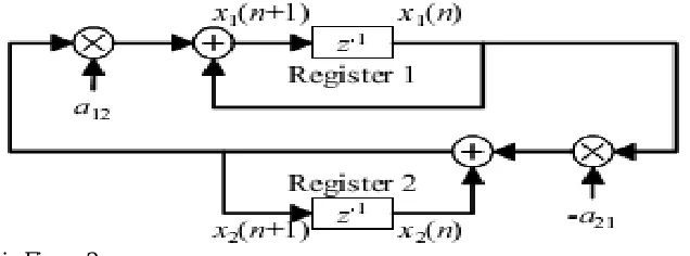
To test analog devices, it is necessary to have trustful and highly configurable analog stimulus and reference signals. In this section, we present a sigma-delta modulation based signal generator to generate reliable analog sinusoidal signals with easily adjustable frequencies. Except for an analog low pass filter, all the added circuits are digital circuits and thus it is easier to integrate the function in silicon and to verify itself before testing the A/D converters. For on-chip test stimulus generation, we start with a digital resonator based on a Lossless Discrete Integrator (LDI) biquad circuit [9]. The resonators are formed by cascading two discrete-time integrators of the form z-1/ (1-z-1) and 1/ (1- z-1) in a loop with the sign of one integrator being positive and the other negative. This
arrangement is shown in Figure 2.
[image:3.612.130.448.574.692.2]Technology (IJRASET)
Two facts are important for the digital resonator. The first one is that variations in the coefficients a21and a12 may cause shifts in the
oscillation frequency. Assuming the resonator is clocked at a rate fos= 1/T, the oscillation frequency ω0will take the following form
[9]:
[image:4.612.170.441.312.506.2]
The second fact is that the amplitude (A) and phase (φ) of the oscillating tone depend on the initial conditions imposed on registers x1and x2. Precisely, it will be [9]:
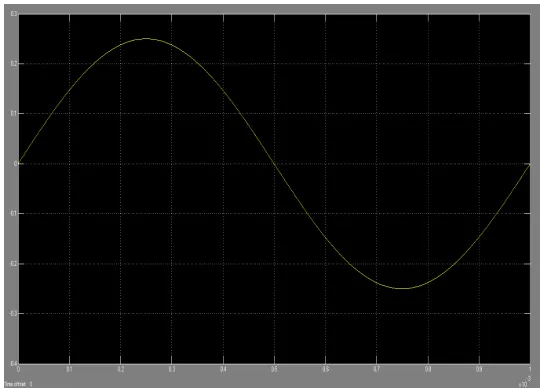
[image:4.612.100.486.556.697.2]Fig. 3. Output of Stimulus Generator, F=1k, Amplitude=.25.
Technology (IJRASET)
When we use Graphical User interfacing of test stimulus generator then GUI needs four inputs. They are 1) Bandwidth, 2) Oversampling Ratio, 3) Number of samples and 4) constant. These all inputs are very closely related to Sigma Delta analog to digital converter.
The basic GUI performs the following function
A. For giving the inputs: following figure 5 it is clearly shown that 4 inputs namely Bandwidth, Oversampling Ratio(R), No. of
Samples (N) and constant are inputs.
B. For generating the Simulink Model : After applying the inputs the START Tab will open the Simulink model as shown below
C. For getting the outputs: After the Simulink model runs we will get the output in the GUI.
Relation between inputs and Sigma Delta analog to digital converter -
Bandwidth (BW) =20000Hz.
Oversampling Ratio(R) =256.
Sampling Frequency= R*2*BW=1024000Hz.
Constant (a21) =.002720171.
Constant (a12) = 2-6.
Fout=10625Hz.
Fout shows the frequency of generated test stimulus.
Fig. 5. Setup of GUI. Fig. 6. GUI of test stimulus generation.
VI. CONCLUSION
The generated test stimulus is trustful and highly configurable analog stimulus. The generated stimulus can used to find the static (offset error, gain error, integral nonlinearity error and differential nonlinearity error) and dynamic (signal to noise ratio, effective no. of bits and signal to noise and distortion ratio) parameter of the sigma delta analog to digital converter.
The graphical user interface providing extra flexibility and playing a very important role in Built in Self-test.
REFERENCES
Technology (IJRASET)
[2] M. Burns, and G. Roberts, an Introduction to Mixed-Signal IC Test and Measurement, Oxford University Press, 2001.
[3] M. L. Bushnell and V. D. Agrawal, Essential of Electronic Testing for Digital, memory & Mixed-Signal VLSI Circuits, Kluwer Academic Publishers, 2000. [4] Evan M. Hawrys hand Gordon W. Roberts. (June 1998),”An Integration of Memory Based Analog Signal Generation into Current DFT Architectures”, IEEE
Transactions on Instrumentation and Measurement, Vol. 47, No. 3.
[5] Dufort, B. & Roberts, G. W. (1999) “On-Chip Analog Signal Generation for Mixed-Signal Built-In Self-Test”. IEEE Journal of Solid-State Circuits, 34, 318-330.
[6] K. Abbes, A. Hentati, M. Masmoudi (2008), “Test and Characterization Of 1bit Sigma Delta Modulator”, 5th International Multi-Conference on Systems, Signals and Devices.
[7] Yun-Che, W. & Kuen-Jong, L. (2000) "An On-Chip ADC Test Structure. Proceedings of Design”, Automation and Test in Europe.
[8] J. L. Huang, C. K. Ong, And K. T. Cheng (2000), “A BIST Scheme For On-Chip ADC And DAC Testing", Design, Automation And Testing Europe, Pp.216-220.
[9] Kuen-Jong, L., Soon-Jyh, C. & Ruei-Shiuan, T. (2003), “A Sigma-Delta Modulation Based BIST Scheme for A/D Converters”, 12th Asian Test Symposium.
[10] Wang, Y.-S., Wang, J.-X., Lai, F.-C. & Ye, Y.-Z. (2005), “A Low-Cost BIST Scheme For ADC Testing”, 6th International Conference On ASIC.
[11] Chee-Kian, O., Kwang-Ting, C. & Wang, L. C. (2004), “A New Sigma-Delta Modulator Architecture for Testing Using Digital Stimulus”. IEEE Transactions on Circuits and Systems, 51, 206-213.
[12] Rolindez, L., Mir, S., Bounceur, A. & Carbonero, J. L. (2006) “A SNDR BIST for Sigma Delta Analogue-To-Digital Converters”. Proceedings ofthe24th IEEEVLSI Test Symposium.
[13] Nabil Chouba, Laroussi Bouzaida, “A BIST Architecture For Sigma Delta ADC Testing Based On Embedded NOEB Self-test And CORDIC Algorithm”, International Conference On Design & Technology Of Integrated Systems In Nanoscale Era, 2010.