Electrical and Optical Characterization of Mg doping in GaN
E.AZIMAH
1,a, N. ZAINAL
1,b, Z. HASSAN
1,c, A. SHUHAIMI
2,d,
AZLAN BAHRIN
1,e1
Nano-optoelectronics Research and Technology, School of Physics, UniversitiSains Malaysia, 11800 Penang, Malaysia
2
Low Dimensional Materials Research Centre (LDMRC), Department of Physics, Faculty of Science, University of Malaya, LembahPantai, 50603 Kuala Lumpur, Malaysia
Email: [email protected], [email protected], [email protected], [email protected],
e
Keywords: Mg doped GaN, PL, I-V, annealing temperature.
Abstract. Apossible evidence of Mg related emission in Mg doped GaN material is observed inoptical measurement, even without thermal annealing. Meanwhile, the electrical properties of the
sample improve when Ni/Au contact layer was annealed up to 400°C, but degrade at further
temperature. We propose that such behavior isrelated to degradation of surface morphology of metal contact at higher temperature.
Introduction
P-type GaN (p-GaN) is one of the critical elements in development of III-V nitride based devices. Traditionally, magnesium (Mg) is used as a dopant for GaN in order to achieve p-type conductivity. However, producing p-GaN with high hole concentration is quite problematic as the activation energy of the Mg is high (135-160 meV) [1-4]. This is due to the strong bonding of Mg-H complexes. For this reason, the evidence of Mg doping in GaN is difficult to be observed in many measurements. On top of that, the strong bonding of the Mg-H complexes leads to low free carrier concentration, causing the difficulty to obtain an excellent Ohmic contact on Mg doped GaN with low resistance.
Here, we investigate the properties of Mg doped GaN using a commercial sample, which was grown by metal-organic chemical vapor deposition (MOCVD). The optical measurement via photoluminescence (PL) allows us to observe the evidence of Mg incorporation in the GaN sample. Further, the ability of the sample to achieve good electrical characteristic will be determined using
current-voltage (I-V) measurements. The factors that affect the electrical characteristic of the
samples are proposed.
Materials and Method
In this work, we used a commercial Mg doped GaN sample grown on sapphire substrate. The
doping concentration of the sample is ~1017cm-3. At the first stage, the sample was measured using
PL measurement and the results were analyzed so that the evidence of incorporation of Mg in the GaN can be identified. The experiment was conducted at room temperature with the excitation wavelength of 325 nm. Next, Ni-Au metal layers were deposited on the sample using thermal evaporator and annealed at different temperatures (in nitrogen gas ambient) in order to increase the diffusion of the metal contact into the sample. Next, the electrical properties of the sample were
measured by I-V measurement. In this experiment, a positive bias is applied on the top of the
sample, hence allowing electrons to be injected from the bottom contact. Such condition is operated under forward bias. Results from this measurement will identify the electrical contact characteristics of the sample; either it has ohmic or shottky characteristics. The change of the electrical behavior of the sample with the annealing temperature was discussed.
Result and Discussion
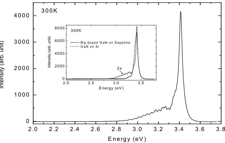
Optical properties. Fig. 1 shows the PL spectrum of the Mg doped GaN sample. Clearly, there is a broad peak around 3.0 to 3.3 eV. We suspect that the transitions from the Mg impurities level may also contribute to this peak. To support this, wehad measured PL of an undoped GaN on Si substrate, whichistypically, has higher density of defects and impuritiesthan mostGaN sampleson sapphire substrate. The PL for both samples is compared and the result isshown in the insert figure of Fig.1. It can be seen that the strong peak near band edge emission in GaN/Si sample is broader than that of the Mg doped GaN and it is shifted to lower energy. These indicate that there are high defects and impurities in the GaN/Si sample. In contrast, on the lower energy side, Mg doped GaN sample exhibits abroader emission peak as compared to the GaN/Si sample. This shows that there is possibility that thetransition from Mg levelalso contributes to the emission. In addition to that, such behavior proposes that our sample does not require a thermal annealing process to activate the Mg acceptor, as has been reported in [5]. On another matter, the yellow band emission, which is typically observed at 2.5 eV is almost invisible in the spectrum.
2 .0 2 .2 2 .4 2 .6 2 .8 3 .0 3 .2 3 .4 3 .6 3 .8
0 1 0 0 0 2 0 0 0 3 0 0 0 4 0 0 0
2 .0 2 .5 3 .0 3 .5
0 2 0 0 0 4 0 0 0 6 0 0 0 8 0 0 0
In te n s it y ( a rb . u n it )
E n e rg y (e V ) 3 0 0 K
M g d o p e d G a N o n S a p p h ire G a N o n S i
In te n s it y ( a rb . u n it )
E ne rg y (e V ) 3 0 0 K
[image:2.595.84.466.293.536.2]2 x
Fig. 1: PL spectrum of the Mg doped GaN sample. Insert figure shows the comparison of PL for the Mg doped sample and the undopedGaN on Si sample.
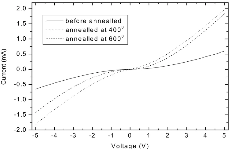
Next, the electrical properties of the Mg doped GaN samples were investigated via I-V
measurement. Prior to this work, Ni (~0.6µm)-Au (~0.3µm) metal bi-layers were deposited onto the
sample using thermal evaporator. The sample was then annealed at different temperature.Changing
in temperature results in different I-V characteristic of the sample and this is shown in Fig. 2.
Clearly, the sample shows good electrical properties when it was heated up to 400°C. However,
On the other matter, it is worth to note that theI-V curves do not show Ohmic characteristic at all. This issue may relate to the use of nitrogen gas during the anneal process. Instead, we suggest that oxygen gaswould promote good Ohmic characteristic to the sample as the gas will introduce a p-type Ni-oxide layer between Ni and p-GaN [6, 7]. Such layer carries high hole density that makes less resistanceto the current tobe injected to the sample.
Fig. 2: I-V characteristic of the Mg doped GaN sample annealed at different temperature.
Obviously, the electrical properties of the sample behave differently with temperature.
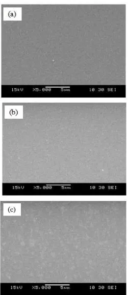
Fig. 3 shows the surface morphology of the metal contact layers on the sample with the variation of annealing temperature. Detailed investigation found that the surface becomes smoother when the
sample was annealed up to 400°C. At this temperature, the electrical contact of the sample is
improved due to the increase of the metal diffusion into the sample. However, the surface
morphology of the metal layers degrades at 600°C, as shows Fig. 3c.This may lead to the
fluctuation of the metal layers and surface roughness, and hence reduces the electrical properties of the sample. Degradation of surface morphology of the Ni-Au metal layers on p-GaN samplesat higher temperature has been reported across literature, see example [8, 9].
-5 -4 -3 -2 -1 0 1 2 3 4 5
-2 .0 -1 .5 -1 .0 -0 .5 0 .0 0 .5 1 .0 1 .5 2 .0
b e fo re a n n e a lle d
a n n e a lle d a t 4 0 00
a n n e a lle d a t 6 0 00
C
u
rr
e
n
t
(m
A
)
Fig. 3: SEM images of surface morphology of the Ni-Au metal layers on the Mg dopedGaNsample
at different annealing temperature. (a) before annealed, (b) annealed at 400°C and (c) annealed at
600°C.
Conclusion
The possibility that Mgplayed a role in the optical transitions in the Mg doped GaN sample was
observed in the PL measurement. A Ni-Au layer was deposited onto the sample and its
I-Vproperties degraded as the temperature increased. The degradation of surface morphology might
Acknowledgement
This work was supported by Universiti Sains Malaysia Short Term Grant under account number 304/PFIZIK/6311066 and Fundamental Research Grant Scheme under account number 203/PFIZIK/6711261. The authors would like to acknowledgetechnical support from NOR Lab staff is gratefully acknowledged.
References
[1] N.A. Reshchikov and J. HadisMorkoç: Appl. Phys. Vol. 97 (2005), p. 061301.
[2] L. Yow-Jon: Appl. Phys. Lett. Vol. 84 (2004), p. 2760 .
[3] Y. Nakano and T. Jimbo: J. Appl. Phys.Vol. 92 (2002), p. 5590 .
[4] R. Kudrawiec, M. Motyka, J. Misiewicz, B. Paszkiewicz, R. Paszkiewicz and M Tłaczała,J:
Phys. D: Appl. Phys.Vol. 41 (2008), p. 165109 .
[5] C. Guarneros and V. Sánchez: Material Science and Engineering B Vol. 174 (2010), p. 263
[6] J.O. Song, D.E. Leem, S.H. Kim, J.S. Kwak, O.H. Nam, Y. Park, T.Y. Seong, Solid-State
Electronics Vol. 48 (2004), p. 1597 .
[7] R.H. Jorng, D-S Wuu, Y-C Lien and W-H. Lan: Appl. Phys. Lett.Vol. 79 (2001), p. 2925
[8] H. Chin-Yuan, L. Wen-How and S.Y. Chung, and S. Wu: Appl. Phys. Lett.Vol. 83 (2003),
p. 2447.
[9] J.Y. Moon, J.H. Kim, H.S. Lee, C.H. Ahn and H.K. Cho, J.Y. Lee and H.S. Kim: Journal of