NoC based Efficient RTL Design and Verification of
SoCWire BUS Protocol
Nitin Kumar
Tiwari
Department of Electronics & Communication Dr. B. R. Ambedkar National Institute of
Technology Jalandhar (India)
Ravi Kumar
Department of Electronics & Communication Dr. B. R Ambedkar National Instituteof
Technology Jalandhar (India)
R. K. Sarin
Department of Electronics & Communication Dr. B. R. Ambedkar National Institute of
Technology Jalandhar (India)
Sarabjeet Singh
Department of Physics Dr. B. R. Ambedkar National Institute of
Technology Jalandhar (India)
ABSTRACT
System on Chip Wire (SoCWire) is a Network on Chip (NoC) based design that composed of intellectual property blocks (IP) and interconnects based on space wire standard, was successfully implemented in Venus Express Monitoring Camera (VMC) mission and proposed to implement in Solar Orbital mission in future. The efficient and accurate implementation of SoCWire is the main concern in this work. A solution for single bit error detection and correction with hamming code for 8 bit data has been proposed, so that the accuracy of the design is improved with cost of extra resources and we can save nearly 19.2 μs time that is required to link re-initialization also the speed of the design is improved compared to conventional Codec. For routing data of many codec from one node to many other nodes SoCWire Switch is implement with crossbar based switch for 8 ports and achieved maximum frequency 179.743 MHz and 5% device utilization can be saved compared to [1]. These functionality and design performance are achieved with coding level change in VHDL for SoCWire. The design is synthesized on Xilinx ISE 12.1. The Target FPGA is XCVLX-60 which belongs to Xilinx Virtex 4 QPro.
Keywords
SoCWire, Hamming code, Crossbar and packet
1.
INTRODUCTION
Single chip integrated circuits are commonly referred to as system-on-chip (SoC), and typically consist of several complex heterogeneous components have fueled the need for complex chips that incorporate multiple processors dedicated for specific computational needs [1]. NoC-based SoC design uses packet transactions rather than circuit transactions, and there is a distributed network structure instead of a conventional globally shared bus or a centralized matrix. In NoC-based SoC design each of the functional modules should be designed to be latency-insensitive to support packet transactions which improve reliability and the speed of interconnection links, efficient link utilization is another advantage because only one part of the end-to-end path between functional modules is occupied by the traversing packets. For all these reasons, advanced bus architectures are gradually considering a packet transaction concept into their protocols [2, 3]. NoC-based SoC design based on space wire interface standard of ESA (European Space Agency) supports packet transactions and known as SoCWire [4]. The advantageous features of the SpaceWire standard including
flow control and hot-plug ability and the error detection was still fully supported with easy implementation of standard Xilinx Bus- Macros [5]. The SoCWire architecture composed of SoCWire Codec and SoCWire Switch. SoCWire CODEC connects a node or host system to a SoCWire network and developed in a complete synchronous VHDL model. SoCWire Switch enables the transfer of packets arriving at one link interface to another link interface on the switch was realized by internal SoCWire Codecs. The main difference between SpaceWire and SoCWire was the parallel data transfer and the complete synchronous implementation of SoCWire. Therefore SoCWire is more deterministic because any change of state is related to clock cycles. The overall link initialization requires minimum time of ‘19.2 μs’ [6]. SoCWire Codec operation controlled with a state machine parity bit concept was used to detect transmission errors at link initialization or at the run state of a SoCWire. For 8 bit data word width 10 bit wide packet (1 bit parity, 1 bit data control flag, 8 bit data) as shown in figure 1 was used for link initialization of CODECs.
MSB LSB
D7 D6 D5 D4 D3 D2 D1 D0 0 P
Data Control Flag
[image:1.595.311.549.484.597.2]Parity Bit
Figure 1 SoCWire Packet for interface [1]
To overcome the problem of link initialization we proposed a new framework for 8 bit data using hamming code.
Concept of hamming code
The Hamming single-bit correction code is implemented by adding check bits to the output data packet when the transmitted packet is received parity bit is calculated and stored in a syndrome value. If the syndrome value is „0‟ there have been no errors. Syndrome value identifies the erroneous bit, which needs to be inverted [7]. SoCWire works on odd parity for detection and correction of bit errors [8]. For 8 bit data packet size 13 bits (4 check bit, 8 data bit, and 1 bit data control flag) used as shown in figure [9].
MSB LSB D 7 D 6 D 5 D 4 P 3 D 3 D 2 D 1 P 2 D 0 P 1 P 0 0 Parity bits
Data Control Flag
Figure 2 Proposed SoCWire Packet with hamming code.
[image:2.595.61.280.271.388.2]The SoCWire Switch was fully scalable design supporting data word width (from 8 to 128 Bit) and 2 to 32 ports with low latency and supports wormhole routing and round robin scheduling [10]. In indirect or switch-based networks each connection between nodes has to pass a set of switches each node comprises the processor module and network interface which is connected to a switch as shown in figure 3 [6]. Processor Module Switch Network Interface
Figure 3 Crossbar topology [6]
The crossbar topology is especially suitable for the reconfigurable data processing units (such as SoCWire) with macro pipeline that provide isolation of faulty modules [6]. In this work we utilized flexibility of crossbar switch and optimized the performance of SoCWire by transferring codec data upto 8 ports and validate the performance by transferring codec data from one port to another. For future space missions e.g. Solar Orbiter, the demand for high performance onboard processing has drastically increased. By using capabilities for in flight re-configurability of data processing units based on FPGA system maintenance and performance enhancement on board can be achieved [11]. In this paper we implement Modified SoCWire and compare its performance with the conventional SoCWire. The paper is organized as following Section 2, present design and implementation of SoCWire Codec and SoCWire Switch. Section 3 gives comparison based on simulation results of Modified SoCWire with conventional SoCWire.
2.
DESIGN AND IMPLEMENTATION
OF SoCWire
In this section design and implementation of SoCwire is given, in first part design process of SoCWire Codec is described and implemented. Design and implementation of SoCWire Switch is given in the next part.
2.1
Design of SoCWire Codec
Space Wire interface is a well established standard, providing a layered protocol (physical, signal, character, exchange packet, network) and proven interface for space applications. The SoCWire character level, exchange level, packet level and network level is derived from the SpaceWire standard. Flow Control Token (FCT), End of Packet (EOP), Error End
of Packet (EEP) and an Escape Character (ESC) are 4 bit length control characters for flow control. Flow Control Token (FCT) manages the flow of data, indicating Space for 8 more normal-characters in the receiver buffer. Regular packets completed with an EOP marker. EEP marker sends by indicate an erroneous packet and target reject the packet. Escape Character (ESC) is used to form the higher level control code (8 bit length). Null is formed by the combination of escape and FCT control code (ESC + FCT). The controlled operation and link initialization sequence of SoCWire Codec is shown by sate diagram in figure 4.
The initial state of SoCWire Codec is “ErrorReset” after link reset, by de-asserting reset and delay of „6.4 μs’ state moves to “ErrorWait” at ErrorWait a delay of ‘12.8 μs’ was taken for next state to move. The link was established for transmission that both ends of the link are ready to receive data after that time. The “Ready” state has the permission for link set up and state moves to “Started” state and waits „12.8 μs’ for NULL-characters. After reception of NULL characters state moves into “Connecting” and wait upto ‘12.8 μs’ for FCT. By receiving FCT state goes to “Run” state and normal operation of SoCWire codec was started. If an Rxerror occurs at any state of Codec during link initialization the operation was terminated and codec state forced to move on Error Reset state. For critical space mission or real time operation this situation becomes critical due to loss of data if link connection re-started. These errors are generally bit error we used hamming code for bit error detection and correction for 8 bit data and save the link initialization time approximately ’19.2 μs’ time with Modified SoCWire Codec based on Proposed SoCWire Packet with hamming code. The comparative results of modified SoCWire Codec with conventional Codec in form of devices utilization and speed are given in Table 1.
Reset
After 6.4 us Disable
Rx_err
Rx_err Rx_err Rx_err got_fct got_fct got_fct
got_ fct 12.8 us 12.8 us 12.8 us after12.8 us
got_Null enable
Figure 4 SoCWire Codec State Machine.
Error Reset
Run Error
Wait
Ready
Conne-cting
Table 1 Device utilization summery of SoCWire Codec with 8 bit data
Parameter
Conventional SoCWire Codec [10]
Modified SoCWire Codec with Hamming code
Slices 180 181
Flip Flops 143 166
4 input LUTs 340 341
Maximum Frequency (MHz)
219.450 224.369
2.2
Design of SoCWire Switch
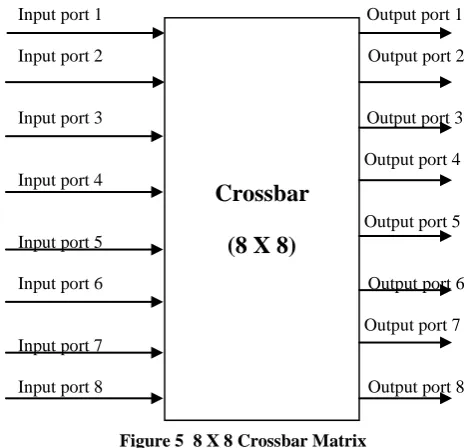
NoC based and reconfigurable computing design has implemented in on-chip programmable interconnects. The interconnect structure significantly affect area and speed. For a network a packet oriented protocol and a switch is required for routing many codec data from one node to many nodes. The packet oriented switch contains <destination address + cargo + end of packet>. Destination address in the port number of output port, cargo is the data to be send and end of packet indicate that the data has been send to the specified port or indicate an erroneous packet and terminated the operation for further destination address search. In the direct port addressing packets with crossbar switch packets are routed directly to one of the output port to others with the port addresses. As the destination port address and input port address is matched packet routed immediately to that output port address and thus that port is marked as busy and cannot be accessed until the end of the packet is received. The 8x8 crossbar matrix implemented in this work as SoCWire Switch is shown in figure 5.
Input port 1 Output port 1 Input port 2 Output port 2
Input port 3 Output port 3 Output port 4 Input port 4
Output port 5 Input port 5
Input port 6 Output port 6 Output port 7 Input port 7
[image:3.595.45.279.475.699.2]Input port 8 Output port 8
Figure 5 8 X 8 Crossbar Matrix
The SoCWire consists of a number of SoCWire Codec according to the number of ports of Switch and additional fully pipelined control machines. The SoCWire Switch has been implemented on Xilinx Virtex-4 LX60-10. Table 2 shows the device utilization summery and maximum frequency of Modified SoCWire for transferring 8 bit data to
8 ports of switch. It is implemented by Modified SoCWire Codec and crossbar based switch.
Table 2 Device utilization summery of SoCWire with 8 bit data and 8 ports
Parameter
Conventional SoCWire (Codec + Switch) [10]
Modified SoCWire (Modified SoCWire Codec + Crossbar based switch)
Slices 2204 2096
Flip Flops 1512 2100
4 input LUTs 4139 3915
Maximum Frequency (MHz)
157.306 179.743
3.
SIMULATION RESULTS OF SoCWire
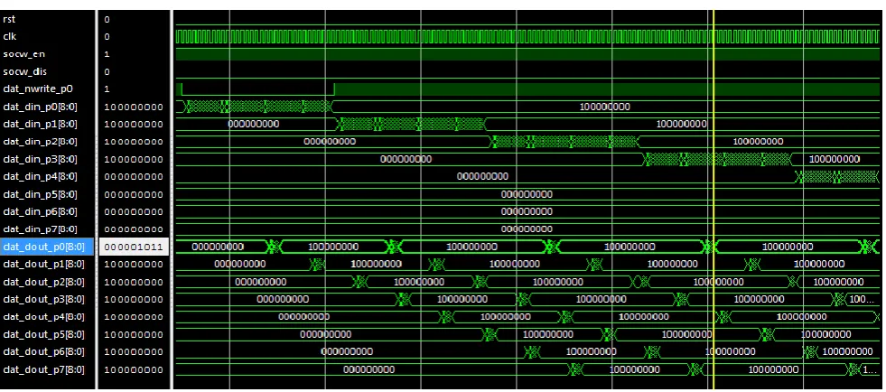
Verification of the system architecture was done using Xilinx ISE 12.1 and ISIM Simulator. Figure 6 shows the waveform of SoCWire Codec when parity Error was detected the waveform clearly shows that when parity error was high the Codec state jump to “ErrorReset” of Codec State machine. For proper operation of SoCWire first of all link connection is established for that state of the codec should be “Run” state so that parity error must be corrected. To overcome this and to improve the performance of SoCWire Codec hamming code concept for 8 bit data is used with VHDL coding level changes and implemented as Modified SoCWire Codec and got high speed with accurate design as the error detected and corrected at run time. The simulated waveform of it is shown in figure 7. SoCWire Switch simulated waveform for transferring Modified SoCWire Codec data is shown in figure 8 in this waveform dat_din_p0 to dat_din_p7 are input data port and port dat_dout_p0 to dat_dout_p7 are output ports. Data from one port to other was send with port address and terminated at end of packet. The SoCWire Switch was verified by transferring data randomly from one input port to all output port and respectively for the other input ports.
4.
CONCLUSION
SoCWire was successfully implemented in space in Venus Express mission and proposed to implement in Solar Orbiter mission in near future. SoCWire IP was available to us we use the same IP and proposed a solution for single bit error detection and correction with hamming code for 8 bit data in Modified SoCWire Codec so that the accuracy of the system is improved with cost of same extra resources but these are available enough on our target FPGA and we can save nearly ‘19.2 μs’ time which plays a vital role on such critical mission or real time operation also the speed of the design is improved. For routing data of Modified SoCWire Codec for routing data from one codec to others SoCWire Switch is implemented with crossbar based switch and achieved maximum frequency 179.743 MHz with Modified SoCWire (Modified SoCWire Codec + crossbar based Switch) which is 22 MHz faster than the conventional SoCWire and the overall devices requirement in terms of slices and LUTs is 5% less compared to conventional SoCWire for routing 8 bit data to 8 port via switch. So that for higher frequency requirement this modification can be used. The proposed design was implemented for 8 bit data and for 8 port of Switch. In future,
error detection and correction of larger data width and to transfer this data for large number of ports will be implemented
.
Figure 6 Waveform of SoCWire codec with parity error.
Figure 7 Waveform of SoCWire Codec after removed parity error with applying hamming code.
[image:4.595.55.546.531.748.2]5.
REFERENCES
[1] B. Osterloh, “SoCWire User Manual”, www.socwire.org, 2009.
[2] Sudeep Pasricha, Nikil Dutt,“On-Chip Communication Architectures”, Morgan Kaufmann Publications, U.S, 2008.
[3] P. Guerrier and A. Greiner, “A Generic Architecture for On-Chip Packet-Switched Interconnections,” Proc. Design, Automation and Test in Europe (DATE ‟00), pp. 250-256, Mar. 2000.
[4] ECSS, Space Engineering: SpaceWire–Links, nodes, routers, and networks, ESA-ESTEC, Noordwijk
Netherlands, ECSS-E-50-12A, (January 2003).
[5] SM Parkes “ECSS, Space Engineering: SpaceWire:SERIAL POINT-TO POINT LINKS”, ESA- ESTEC, , Dundee, ECSS-E-50-12A,(January 2000).
[6] Bjorn Osterloh, Harald Michalik, Björn Fiethe, Frank Bubenhagen “Architecture Verification of the SoCWire NoC Approach for Safe Dynamic Partia Reconfiguration in Space Applications” NASA/ESA
Conference on Adaptive Hardware and Systems (AHS 2011), Sep 2010.
[7] U.K. Kumar, B.S Umashankar “Improved Hamming Code for Error Detection and Correction”, ISWPC, pp. 498-500, 2007.
[8] U.K. Kumar, B.S Umashankar “Improved Hamming Code for Error Detection and Correction” ISWPC-2007.
[9] Simon Tam, “Single Error Correction and Double Error Detection”, Application Note: Virtex-II Pro, Virtex-4, and Virtex-5 Families, Xilinx XAPP645 (v2.2) August 9, 2006.
[10] B. Osterloh, H. Michalik, B. Fiethe, F. Bubenhagen, “Enhancements of reconfigurable System-on-Chip Data Processing Units for Space Application”, AHS‟07. pp. 258-262, Second NASA/ESA Conference on Adaptive Hardware and Systems (AHS 2007), Edinburgh, August 2007.
![Figure 1 SoCWire Packet for interface [1]](https://thumb-us.123doks.com/thumbv2/123dok_us/8119779.793832/1.595.311.549.484.597/figure-socwire-packet-for-interface.webp)
![Figure 3 Crossbar topology [6]](https://thumb-us.123doks.com/thumbv2/123dok_us/8119779.793832/2.595.61.280.271.388/figure-crossbar-topology.webp)