Design and Optimization of n-bit Reversible
Binary Comparator
Rangaraju H G
Department of Electronics andCommunication Engineering, Government Engineering
College,
Chamarajanagar 571313, India
Vinayak Hegde, Raja K B
Department of Electronics and Communication Engineering,University Visvesvaraya College of Engineering, Bangalore – 560001, India
Muralidhara K N
Department of Electronics andCommunication Engineering, P E S College of Engineering,
Mandya 571401, India
ABSTRACT
Reversible logic has attracted significance attention in recent years, leading to different approaches such as synthesis, optimization, simulation and verification. In this paper, we propose the design and optimization of n-bit reversible binary comparator. The circuit for MSB and one-bit comparator cell using NOT, PG and CNOT gates are designed. The n-bit reversible binary comparator is designed using circuit for MSB as first stage to compare MSBs and one-bit comparator cell as second stage and so on to compare lesser significant bit positions. The power consumption, delay, garbage outputs and constant inputs are computed. It is observed that the quantum cost and garbage output values are less in the proposed technique compared to the existing approaches.
KEYWORDS
Reversible Binary Comparator, Quantum Cost, Reversible Logic, Garbage Output, Constant Input.
1.
INTRODUCTION
Power dissipation, silicon area and delay are major issues in VLSI design. The more number of devices are fabricated in a small silicon area to reduce size of equipment used in the real time applications. The power dissipation increases since the heat developed by more number of devices in the system. The disadvantages of real time application equipment’s are (i) Increase the cost of cooling and packaging, (ii) performance of the circuit deteriorates and (iii) spoils the environment by global warming. Power consumption in CMOS design is of three types: static, short-circuit and dynamic power. Static power consumption is due to transistor leakage current, is the sum of leakage and all biased currents. Short-circuit power is related to supply voltage and threshold voltage of transistor, is determined by the process. Dynamic power is the power consumed during switching events in the core or input/output of the design. Switching activity is function of voltage, frequency and capacitance.
The dynamic power is the charging and discharging of parasitic gate capacitance and metal layers, which is dominant among the overall power consumption of the chip. Hence most of the designer’s effort goes on reducing dynamic power, which includes the reduction of capacitance, operating voltage, frequency and switching. With advancement in technologies, ASIC and FPGAs have increased in logic capacity and performance. Power consumption is receiving greater attention at the component selection phase of ASIC and FPGA-based designs. Due to exponential growth, physical boundaries will be reached in the near future hence traditional technologies like CMOS will reach their limits. To overcome this, an alternative computation technologies are required that encourages research in reversible logic.
Reversible computing has become a strongly studied research area. As reversible circuits are subjected to certain restrictions like fan-out and feedback, synthesis aspects are of interesting. According to Landauer [1], every bit of information lost consumes KTln2 joules of energy, where K is Boltzmann’s constant and T is the absolute temperature at which the operation performed. Charles Bennett [2] showed that if the computation is carried out in reversible logic, the energy loss can be reduced or even eliminated and also proved that circuits built from reversible gates have zero power dissipation.
The recycling of real life entities like bottles, cans, paper etc., were impossible decades back, but they are quite prominent today. The same applies to the computing world also. Today’s computers consume huge amount of energy, as millions of bits are manipulated billion times in every second. The irreversible logic devices are used in computers been recognized as energy inefficient for several decades. The reversible computing, which does not compute bits that are no longer needed, that allows their energy to be recovered and recycled for use in later operations. The demand for energy efficient becomes more prominent hence reversible computing will become popular. Before the computer industry reaches the fundamental brick wall of performance and energy constraints of computing devices, reversible computing needs to be fully developed.
Organization: The paper is organized into the following sections. Section 2 is an overview of basic reversible gates. The literature survey is described in section 3. Section 4 is the proposed comparator design, result analysis of the proposed design is presented in section 5 and conclusions are contained in section 6.
2.
BASIC REVERSIBLE GATES
The simplest reversible gate is NOT gate and is a 1*1 gate. Controlled NOT (CNOT) gate is an example for a 2*2 gate. There are many 3*3 reversible gates such as Fredkin (F), Toffoli (TG), Peres (PG) and TR gate. The quantum cost of 1*1 Reversible gates is zero, and quantum cost of 2*2 reversible gates is one. Any reversible gate is realized by using 1*1 NOT gates and 2*2 reversible gates, such as V, V+ (V is square root of NOT gate and V+ is its hermitian) and Feynman gate which is also known as CNOT gate. The V and V+ quantum gates have the property given in the Equations 1, 2 and 3.
V * V = NOT ……… (1) V * V+ = V+ * V = I ……….. (2) V+ * V+ = NOT ………. (3)
The quantum cost of a reversible gate is calculated by counting the number of V, V+ and CNOT gates.
2.1 NOT Gate
A P = A′
[image:2.595.321.530.107.246.2]
Figure 1. NOT Gate.
The reversible 1*1 gate is NOT gate with zero quantum cost is as shown in the Figure 1.
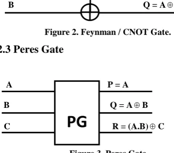
2.2 Feynman / CNOT Gate
The reversible 2*2 gate with quantum cost of one having mapping input (A, B) to output (P = A, Q = AB) is as shown in the Figure 2.
A P = A
[image:2.595.54.234.356.417.2]B Q = AB
Figure 2. Feynman / CNOT Gate.
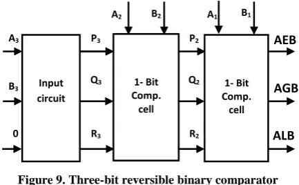
2.3 Peres Gate
A P = A B Q = AB C R = (A.B)C
Figure 3. Peres Gate
The three inputs and three outputs i.e., 3*3 reversible gate having inputs (A, B, C) mapping to outputs (P = A, Q = A B, R = (A.B)C). Since it requires two V+, one V and one CNOT gate, it has the quantum cost of four. The Peres gate
[7] and its quantum implementation are as shown in the Figure 3 and 4 respectively.
A P = A
B Q = AB
[image:2.595.57.234.547.703.2]
C R = (A.B)C
Figure 4. Quantum implementation of Peres Gate
3.
LITERATURE SURVEY
Zeljko Zilic et al., [8] presented a methodology for realizing the networks of reversible gates results in synthesizing complex reversible circuits by mapping the original irreversible circuit specification into a library of reversible cells. Mozammel Khan [9] explained the design of quantum ternary equality, less-than and greater-than comparator using one-qutrit and two-qutrit Muthukrishnan-stroud gates, which are multi-valued quantum gates. Zichu Qi et al., [10] presented a floating-point Fused multiply-add unit with low-cost and low-power techniques. To reduce area for supporting two single precision operations in parallel, the multiplier, shifter and adder are reused. Leland Chang et al., [11] explored about the limitations of power dissipation due to advancement in silicon microelectronics and the importance of trade-off between power and performance and also shown that area is the constraint in improving power efficiency. Fuming Sun et al., [12] analyzed the sources of power consumption, design consideration, technologies and analysis tools in FPGA. A general view of power consumption, various forms of power consumption and design characteristics to minimize power consumption are discussed. Michael Miller and Zahra Sasanian [13] explained cost saving with the goal of reducing the number of quantum gates required, based on novel line labeling and gate moving procedures. Maii Emam and Layle Elsayed [14] presented two novel designs of adder/subtractor using reversible gates. First design uses two’s complement adder/subtractor suitable for signed/unsigned numbers. Other one is a novel reversible gate that can work singly as reversible full adder/subtractor unit. The design is extended for reversible four-bit ripple adder/subtractor. Madhusmita Mahapatro et al., [15] developed a reversible counterpart of all the irreversible basic logic gates and full custom layout of all these gates with reversibility using 0.25 µm technology. The reversible full adder, half adder, four-bit binary parallel adder and 4x4 multiplier circuits are designed using reversible logic. Lihui Ni et al., [16] proposed a general approach to construct the reversible full-adder with two reversible gates and two garbage outputs. The reversible full adder can be used to construct the large-scale reversible systems and can reduce the cost of the circuits.
Mathias Soeken et al., [17] introduced Revkit, a toolkit that helps to make recent developments in reversible circuit design accessible to others. A modular and extendable framework is provided which enables the addition of new methods and tools. Stefan Frehse et al., [18] presented an automatic debugging approach for reversible logic, based on simulation with pattern matching. In many cases this leads to significant
PG
[image:2.595.59.225.623.709.2]reductions of the number of errors. Applying this leads to run time improvements up to five orders of magnitude. Rangaraju et al., [19] proposed three designs of reversible parallel binary adder/subtractor which is used for low-power applications and is efficient in terms of quantum cost, number of gates used, garbage inputs/outputs. Praveen et al., [20] presented a 4x4 reversible adder/subtractor circuit which performs half/full adder and subtractor function with minimum garbage count and critical path.
4. PROPOSED COMPARATOR DESIGN
4.1 Circuit for MSB
The circuit for MSB is to binary comparator using reversible logic is shown in Figure 5. This circuit consists of three inputs An, Bn and logical low i.e., 0 and the outputs A Equal to B
[image:3.595.310.554.103.530.2](AEB), A Greater than B (AGB) and A Less than B (ALB). The reversible circuit for MSB is designed using one PG, two CNOT and one NOT gates. The circuit for MSB alone can function as one-bit comparator and has one garbage output, two constant inputs and the quantum cost of six as PG gate costs four and each CNOT gate costs one. This circuit for MSB is connected at the first stage of the serial design of n-bit reversible binary comparator.
Figure 5. The circuit for MSB of the reversible binary comparator
The input Bn is connected to the NOT gate to get Bn′ at the
output of the NOT gate and the inputs An, Bn′and logical Low
are connected to PG gate. The output x is garbage output represented as g1 and output y of the PG gate is (AB)′ is connected to input of CNOT1 gate, another input to CNOT1 gate is Logical High i.e., 1. The output z of the PG gate is AB′ and output m of CNOT1 is (AB) are connected to inputs of the CNOT2 gate. The final outputs of the circuit for MSB are given in Equation 4, 5 and 6.
AEB = (AB)′ ……….. (4) AGB = AB′………... (5)
ALB = A′B ………. (6)
4.2 One-bit Reversible Binary Comparator
Block A is shown in Figure 6 is used in the one-bit comparator cell, which consists of two NOT, one PG and one CNOT gate. The output i of PG is garbage output and output j of the PG gate is (AB)′ is connected to NOT gate and then to input of the CNOT gate. The output k of the PG gate is
connected to input of CNOT gate which results in C1 i.e., AB′
and C2 i.e., A′B.
Figure 6. Block diagram of block A
[image:3.595.55.274.326.505.2]Figure 7. One-bit reversible binary comparator Table 1. One-bit reversible binary comparator
Inputs Outputs
A B ALB AEB AGB
0 0 0 1 0
0 1 1 0 0
1 0 0 0 1
1 1 0 1 0
One-bit reversible binary comparator consists of three PG and four CNOT gates. It has five inputs viz., Pn (AEB), Qn (AGB),
Rn (ALB), An-1 and Bn-1 and three outputs Qn-1 i.e., AGB, Pn-1
i.e., AEB and Rn-1 i.e., ALB as shown in the Figure 7. In this
PG gates are used to generate the product functions like AB′ and A′B and connecting these to three CNOT gates and one
ALB
R
nAEB
P
nAGB
Q
nm
x
y
z
0
A
n
B
n
g
1
1
CNOT1
PG
CNOT 2
Input circuit
C
1k
j
i
C
2Block A
A
n-1B
n-10
g
1PG
CNOT
Pn-1
Qn-1
Rn-1
C2
C1
Bn-1
An-1
R
n Qn
Pn
g3
g4
g5
0
AGB
ALB
AEB
0
g2PG
PG
CNOT 3 CNOT
1
CNOT 2
1-bit comparator cell
[image:3.595.317.542.565.703.2]NOT gate to get the final outputs of one-bit comparator. This circuit designed to be fit at lesser significant bit positions in n-bit binary comparator. This design has a quantum cost of sixteen as three PG gates costs twelve and four CNOT gates costs four, constant inputs of three denoted as logical Low and five garbage outputs represented as g1 to g5. The corresponding input and output combinations are shown in the Table 1.
4.3 Two-bit Reversible Binary Comparator
Two-bit reversible binary comparator is shown in Figure 8. It has two stages: circuit for MSB stage and one-bit comparator cell stage. The two Most Significant Bits (MSBs) A2, B2 are
applied to circuit for MSB, gives one-bit comparison outputs P2, Q2 and R2. These outputs are connected to one-bit
comparator cell which compares two Least Significant Bits (LSBs) A1, B1 with P2, Q2 and R2.The outputs AEB, AGB
and ALB, are final outputs of the two-bit comparator. This design has the quantum cost of twenty two as circuit for MSB costs six and one-bit comparator cell costs sixteen. The constant inputs i.e., inputs connected to Logical low or Logical high are five numbers and six garbage outputs i.e., unused outputs. Outputs for different input combinations are shown in the Table 2.
[image:4.595.321.538.278.412.2]Figure 8. Two-bit reversible binary comparator Table 2. Two-bit reversible binary comparator
Inputs Outputs
A B
ALB AEB AGB
A2 A1 B2 B1
0 0 0 0 0 1 0
0 0 0 1 1 0 0
0 0 1 0 1 0 0
0 0 1 1 1 0 0
0 1 0 0 0 0 1
0 1 0 1 0 1 0
0 1 1 0 1 0 0
0 1 1 1 1 0 0
1 0 0 0 0 0 1
1 0 0 1 0 0 1
1 0 1 0 0 1 0
1 0 1 1 1 0 0
1 1 0 0 0 0 1
1 1 0 1 0 0 1
1 1 1 0 0 0 1
1 1 1 1 0 1 0
In the table A2, A1 and B2, B1 are two-bit numbers A and B
and depending on the magnitude of these bits any one of the outputs i.e., ALB, AEB and AGB will be Logical high. For example consider the tenth row in the table i.e., A2=1, A1=0
and B2=0, B1=1, here since A2 is the MSB bit of A which is
Logical high and B2 is the MSB bit of B which is Logical low
irrespective of other input bits the result will be AGB.
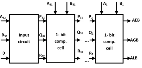
4.4 Three-bit Reversible Binary Comparator
Three stages of three-bit reversible binary comparator is shown in Figure 9. First stage is circuit for MSB stage functions as one-bit comparator compares the MSB bits A3,
B3 of the two numbers. Second stage is one-bit comparator
cell compares the result of the first stage i.e., P3, Q3, R3 and
the input bits A2 and B2. Third stage is also one-bit
comparator cell compares the outputs P2, Q2 and R2 of the
second stage and the LSB bits A1, B1 of the two numbers
results in the final outputs AEB, AGB and ALB of the three-bit comparator.
Figure 9. Three-bit reversible binary comparator
The Quantum Cost (QC) of three-bit reversible binary comparator is given in an Equation:
QC = QC of circuit for MSB + (2 * QC of one-bit Comparator cell) ………. (7)
QC = 6 + 2 x 16 = 38.
The number of Constant Inputs (CIs) of three-bit reversible binary comparator is given in an Equation:
CIs = CIs of circuit for MSB + (2 * CIs of one-bit Comparator cell) ………. (8)
CIs = 2 + 2 x 3 = 8.
The Garbage Outputs (GOs) of three-bit reversible binary comparator is given in an Equation:
GOs = GOs of circuit for MSB + (2 * GOs of one- bit comparator cell) ………..…. (9)
GOs = 1 + 2 x 5 = 11.
4.5 Four-bit Reversible Binary Comparator
Four stages of four-bit reversible binary comparator are shown in Figure 10. First stage is circuit for MSB stage compares the MSB bits of the two numbers. Second stage is one-bit comparator cell compares the result of the first stage and the input bits A2, B2. Third stage is also one-bit
comparator cell compares the output of the second stage and the input bits A1, B1. Fourth stage compares the result of third
stage and the LSB bits A0, B0 of the two numbers resulting the
final output of the four-bit numbers A and B.
ALB
AGB
AEB
B1A1
R2
Q2
P2
B
20
A
2Input circuit 1- bit
comparator cell
ALB AGB AEB B2
A2
R2
Q2
P2
B1
A1
R3
Q3
P3
B3
0 A3
Input circuit
1- Bit Comp.
cell
1- Bit Comp.
[image:4.595.59.274.336.456.2]Figure 10. Four-bit reversible binary comparator
The QC of four-bit reversible binary comparator is given in an Equation:
QC = QC of circuit for MSB + (3 * QC of one-bit Comparator cell) ………. (10)
QC = 6 + 3 x 16 = 54.
The number of CIs of four-bit reversible binary comparator is given in an Equation:
CIs = CIs of circuit for MSB + (3 * CIs of one-bit Comparator cell) ………. (11)
CIs = 2 + 3 x 3 = 11.
The GOs of four-bit reversible binary comparator is given in an Equation:
GOs = GOs of circuit for MSB + (3 * GOs of one- bit comparator cell) ………. (12)
GOs = 1 + 3 x 5 = 16.
4.6 Eight-bit Reversible Binary Comparator
Eight-bit reversible binary comparator is shown in Figure 11. First stage is circuit for MSB stage compares the MSB bits of the two numbers A8, B8. Second stage is one-bit comparator
cell compares the result of the first stage and the input bits A7,
B7. Third stage is also one-bit comparator cell compares the
output of the second stage and the input bits A6, B6. Fourth
stage compares the result of third stage and the input bits A5,
B5 of the two numbers and so on. The final stage compares
the output of the seventh stage and the LSB bits A1, B1
resulting the final output of the eight-bit numbers A and B.
Figure 11. Eight-bit reversible binary comparator
The QC of eight-bit reversible binary comparator is given in an Equation:
QC = QC of circuit for MSB + (7 * QC of one-bit Comparator cell) ……….……. (13)
QC = 6 + 7 x 16 = 118.
The number of CIs of eight-bit reversible binary comparator is given in an Equation:
CIs = CIs of circuit for MSB + (7 * CIs of one-bit Comparator cell) ………..……. (14)
CIs = 2 + 7 x 3 = 23.
The GOs of eight-bit reversible binary comparator is given in an Equation:
GOs = GOs of circuit for MSB + (7 * GOs of one- bit comparator cell) ………. (15)
GOs = 1 + 7 x 5 = 36.
4.7 Sixteen-bit Reversible Binary Comparator
Sixteen stages of sixteen-bit reversible binary comparator are shown in Figure 12. First stage compares the MSB bits of the two numbers A16, B16. Second stage is one-bit comparator cell
compares the result of the first stage and the input bits A15,
B15. Third stage is also one-bit comparator cell compares the
output of the second stage and the input bits A14, B14. Fourth
stage compares the result of third stage and the input bits A13,
B13 of the two numbers and so on. The final stage compares
the output of the fifteenth stage and the LSB bits A1, B1
[image:5.595.309.550.239.353.2]resulting the final output of the eight-bit numbers A and B.
Figure 12. Sixteen-bit reversible binary comparator
The QC of sixteen-bit reversible binary comparator is given in an Equation:
QC = QC of circuit for MSB + (15 * QC of one-bit Comparator cell) ………. (16)
QC = 6 + 15 x 16 = 246.
The number of CIs of sixteen-bit reversible binary comparator is given in an Equation:
CIs = CIs of circuit for MSB + (15 * CIs of one-bit Comparator cell) ………. (17)
CIs = 2 + 15 x 3 = 47.
The GOs of sixteen-bit reversible binary comparator is given in an Equation:
GOs = GOs of circuit for MSB + (15 * GOs of one-bit comparator cell) …………...…. (18)
GOs = 1 + 15 x 5 = 76.
4.8 Thirty-Two-bit Reversible Binary
Comparator
[image:5.595.50.291.507.616.2]Thirty-two-bit reversible binary comparator are shown in Figure 13. First stage is circuit for MSB stage works as one-bit comparator compares the MSB one-bits of the two numbers A32, B32. Second stage is one-bit comparator cell compares the
result of the first stage and the input bits A31, B31. Third stage
is also one-bit comparator cell compares the output of the second stage and the input bits A30, B30. Fourth stage
compares the result of third stage and the input bits A29, B29 of
the two numbers and so on. The final stage compares the output of the thirty-first stage and the LSB bits A1, B1
resulting the final output of the thirty-two-bit numbers A and B.
…
…
Q3 R3…
.
P3 R2 Q2 P2 A3 ALB AGB AEBB3 A1 B1
R4 Q4 P4 B4 0 A4
Input circuit 1- bit comp. cell 1- bit comp. cell
…
…
Q7 R7…
.
P7 R2 Q2 P2 A7 ALB AGB AEBB7 A1 B1
R8 Q8 P8 B8 0 A8
Input circuit 1- bit comp. cell 1- bit comp. cell
…
…
Q15 R15…
.
P15 R2 Q2 P2 A15 ALB AGB AEBB15 A1 B1
Figure 13.
Thirty-two-bit reversible binary comparator
The QC of Thirty-two-bit reversible binary comparator is given in an Equation:
QC = QC of circuit for MSB + (31 * QC of one-bit Comparator cell) ………. (19)
QC = 6 + 31 x 16 = 502.
The number of CIs of Thirty-two-bit reversible binary comparator is given in an Equation:
CIs = CIs of circuit for MSB + (31 * CIs of one-bit Comparator cell) ………. (20)
CIs = 2 + 31 x 3 = 95.
The GOs of Thirty-two-bit reversible binary comparator is given in an Equation:
GOs = GOs of circuit for MSB + (31 * GOs of one-bit comparator cell) ……...…………. (21)
GOs = 1 + 31 x 5 = 156.
4.9 Sixty-Four-bit Reversible Binary
Comparator
Sixty-four-bit reversible binary comparator is shown in Figure 14. First stage is circuit for MSB stage works as one-bit comparator compares the MSB bits of the two numbers A64,
B64. Second stage is one-bit comparator cell compares the
result of the first stage and the input bits A63, B63. Third stage
is also one-bit comparator cell compares the output of the second stage and the input bits A62, B62. Fourth stage
compares the result of third stage and the input bits A61, B61 of
the two numbers and so on. The final stage compares the output of the sixty-third stage and the LSB bits A1, B1
resulting the final output of the sixty-four-bit numbers A and B.
The QC of Sixty-four-bit reversible binary comparator is given in an Equation:
QC = QC of circuit for MSB + (63 * QC of one-bit Comparator cell) ………. (22)
QC = 6 + 63 x 16 = 1014.
The number of CIs of Sixty-four-bit reversible binary comparator is given in an Equation:
CIs = CIs of circuit for MSB + (63 * CIs of one-bit Comparator cell) ………. (23)
CIs = 2 + 63 x 3 = 191.
The GOs of Sixty-four-bit reversible binary comparator is given in an Equation:
GOs = GOs of circuit for MSB + (63 * GOs of one-bit comparator cell) …………...……. (24)
[image:6.595.41.285.79.195.2]GOs = 1 + 63 x 5 = 316.
Figure 14. Sixty-Four-bit reversible binary comparator
4.10 n-bit Reversible Binary Comparator
In n-bit reversible binary comparator first stage is circuit for MSB stage works as one-bit comparator to compares the MSB bits of the two numbers An, Bn. Second stage is one-bit
comparator cell compares the result of the first stage and the input bits An-1, Bn-1. Third stage is also one-bit comparator cell
compares the output of the second stage and the input bits A n-2, Bn-2. Fourth stage compares the result of third stage and the
input bits An-3, Bn-3 of the two numbers and so on. The final
stage compares the output of the (n-1)th stage and the LSB bits A1, B1 resulting the final output of the n-bit numbers A and B.
The QC of n-bit reversible binary comparator is given in an Equation:
QC = QC of circuit for MSB + ((n-1) * QC of one-bit Comparator cell) ………. (25)
The number of CIs of n-bit reversible binary comparator is given in an Equation:
CIs = CIs of circuit for MSB + ((n-1) * CIs of one-bit Comparator cell) ………. (26)
The GOs of n-bit reversible binary comparator is given in an Equation:
GOs = GOs of circuit for MSB + ((n-1) * GOs of one-bit comparator cell) …………...……. (27)
5. RESULT ANALYSIS
5.1 Simulation Results
The simulation is carried out using Cadence Tool and S18 (180nm-Analog Process) Technology. The typical gate delay for the process is given ~ 0.2 pf/gate. The one-bit, two-bit, three-bit and four-bit reversible binary comparators are designed and the schematics are simulated to check the functionality of the design, power consumption and delay. The simulation results of one-bit, two-bit, three-bit and four-bit reversible binary comparator are shown in Figure 15, 16, 17 and 18 respectively.
…
…
Q31
R31
…
.
P31
R2
Q2
P2
A31
ALB AGB AEB
B31 A1 B1
R32
Q32
P32
B32
0 A32
Input circuit
1- bit comp. cell
1- bit comp. cell
…
…
Q63
R63
…
.
P63
R2
Q2
P2
A63
ALB AGB AEB
B63 A1 B1
R64
Q64
P64
B64
0 A64
Input circuit
1- bit comp. cell
[image:6.595.308.556.96.209.2]Figure 15. Simulation result of one-bit reversible comparator
Figure 16. Simulation result of two-bit reversible comparator
Figure 17. Simulation result of three-bit reversible comparator
Figure 18. Simulation result of four-bit reversible comparator
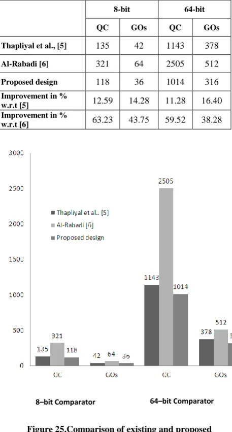
5.2 Performance analysis
The performance of 8, 16, 32 and 64-bit binary comparator design is shown in the table 5. The quantum cost is 118 in case of 8-bit comparator and 246, 502 and 1014 in case of 16, 32 and 64-bit comparator respectively. The number of constant inputs are 23, 47, 95 and 191 in case of 8, 16, 32 and 64-bit comparator respectively. The numbers of garbage outputs are 36 in 8-bit design, 76 in the case of 16-bit, 156 and 316 in the case of 32-bit and 64-bit design respectively.
Table 5. Performance of 8, 16, 32, 64-bit reversible binary comparator
A comparison of the proposed serial design of 8 and 64-bit reversible binary comparator with the existing approaches [5] and [6] is given in table 6. From the table it is evident that the proposed design has an improvement of 12.59% and 63.23% in QC, 14.28% and 43.75% in GOs in the case of 8-Bit. The improvement of 11.28% and 59.52% in QC, 16.40% and 38.28% in GOs in the case of 64-bit comparator w. r. t. the existing techniques [5] and [6] respectively. Figure 25 shows the graphical representation of the existing and proposed reversible binary comparators compared in terms of quantum cost and number of garbage outputs. Therefore proposed design has better performance compared to the existing techniques.
Parameter 8-bit 16-bit 32-bit 64-bit Quantum cost 118 246 502 1014
Constant
inputs 23 47 95 191 Garbage
outputs 36 76 156 316 Delay ( nS) 57.6 120 244.8 494.4
[image:7.595.57.289.281.664.2]Table 6. Comparison of existing and proposed 8-bit and 64-bit reversible binary comparators
6. CONCLUSIONS
In this paper design and optimization of n-bit reversible binary comparator is presented. The design is based on the useful properties of PG gate suitable for comparator. The n-bit reversible binary comparator are designed using circuit for MSB as first stage to compare MSBs and one-bit comparator cell as second stage and so on to compare lesser significant bits. The power consumption, delay, garbage outputs and constant inputs are computed. It is seen that the quantum cost and garbage output values are less in the proposed technique compared to the existing approaches. The design is useful in realizing hardware implementation of the quantum algorithms.
REFERENCES
[1] R Landauer, “Irreversibility and Heat Generation in the Computational Process,” IBM Journal of Research and Development, vol. 5, no. 3, pp. 183-191, July 1961. [2] C H Bennett, “Logical Reversibility of Computation,”
IBM Journal of Research and Development, vol. 17, no. 6, pp. 525-532, November 1973.
[3] M Nielsen and I Chuang, “Quantum Computation and Quantum Information,” Cambridge University Press, 2000.
[4]Kerntopf P, M A Perkowski and M H A Khan, “On Universality of General Reversible Multiple Valued Logic Gates,” Proceedings of the Thirty Fourth IEEE International Symposium on Multiple valued Logic, pp. 68 – 73, 2004.
[5]H Thapliyal, N Ranganathan and Ryan Ferreira, “Design of a Comparator Tree based on Reversible logic,” Proceedings of Tenth IEEE International Conference on Nanotechnology Joint Symposium with Nano, pp. 1113 – 1116, August 2010.
[6]A N Al-Rabadi, “Closed – System Quantum Logic Network Implementation of the Viterbi Algorithm,” Facta Universitatis – ser: Elec. Energ., vol. 22, no. 1, pp. 1 – 33, April 2009.
[7] A Peres, “Reversible Logic and Quantum Computers,” International Journal on Physical Review a General Physics, vol. 32, no. 6, pp. 3266–3276, December 1985. [8] Zeljke Zilic, Katarzyna Radecka and Ali Kazamiphur,
“Reversible Circuit Technology Mapping from Non-Reversible Specifications,” Design, Automation and Test Conference Exhibition, pp. 1 – 6, April 2007.
[9]Mozammel H A Khan, “Design of Reversible/ Quantum Ternary Comparator Circuits,” Published in Engineering Letters, Vol. 16, no. 2, pp. 178 – 184, 2008.
[10]Zichu Qi, Qi Guo, Ge Zhang, Xiangku Li and Weiwu Hu, “Design of Low-Cost High-Performance Floating-Point Fused Multiply-Add with Reduced Power,” Twenty Third International Conference on VLSI Design, pp. 206 – 211, January 2010.
[11]L Chang, D J Frank, R K Montoye, S J Koester, Brian L Ji, P W Coteus, R H Dennard, and W Haensch, “Practical Strategies for Power-efficient Computing Technologies,” Proceedings of the IEEE Journal, vol. 98, no. 2, pp. 215 – 236, February 2010.
[12]Fuming Sun, Haiyang Wang, Fei Fu, and Xiaoying Li, “Survey on FPGA Low Power Design,” IEEE International Conference on Intelligent Control and Information Processing, pp. 547 – 550, August 2010. [13]D Michael Miller and Zahra Sasanian, “Lowering the
Quantum Gate Cost of Reversible Circuits,” Fifty Third IEEE Midwest Symposium on Circuits and Systems, pp. 260 – 263, August 2010.
[14]Maii T Emam and Layle A A Elsayed, “Reversible Full Adder/Subtractor,” Tenth IEEE International Conference on Symbolic and Numerical Methods, Modeling and Applications to Circuit Design, pp. 1 – 4, October 2010. [15]Madhusmita Mahapatro, Sisira Kanta Panda, Jagannath
Satpathy, Meraj Saheel, M Suresh, Ajith Kumar Panda and M K Sukla, “Design of Arithmetic Circuits using Reversible Logic Gates and Power Dissipation Calculation,” IEEE International Symposium on Electronic System Design, pp. 85 – 90, 2010.
[16]Lihui Ni, Zhijin Guan and Wenying Zhu, “A General method of Constructing the Reversible Full-Adder,” Third IEEE International Symposium on Intelligent
8-bit 64-bit QC GOs QC GOs Thapliyal et al., [5] 135 42 1143 378
Al-Rabadi [6] 321 64 2505 512
Proposed design 118 36 1014 316
Improvement in %
w.r.t [5] 12.59 14.28 11.28 16.40 Improvement in %
w.r.t [6] 63.23 43.75 59.52 38.28
[image:8.595.53.282.124.550.2]8–bit Comparator 64–bit Comparator
Information Technology and Security Informatics, pp. 109 – 113, 2010.
[17]Mathias Seken, Stefan Frehse, Robert Wille and Rolf Drechsler, “RevKit: A Tool Kit for Reversible Circuit Design,” Workshop on Reversible Computation, 2010. [18]Stefan Frehse, Robert Wille and Rolf Drechsler,
“Efficient Simulation-based Debugging of Reversible Logic,” Fortieth IEEE Symposium on Multi-valued Logic, pp. 156 – 161, 2010.
[19]Rangaraju H G, Venugopal U, Muralidhara K N and Raja K B, “Low Power Reversible Paralell Binary Adder/Subtractor,” International Journal of VLSI design and Communication Systems (VLSICS) Vol.1, No.3, pp. 23 – 34, September 2010.