The Design of Analog Active Filter with Different
Component Value using Genetic Algorithm
Turgay Kaya
Firat University, Faculty of Engineering Department of Electrical and Electronics
Engineering Elazig/Turkey
Melih Cevdet Ince
Firat University, Faculty of Engineering Department of Electrical and Electronics
Engineering Elazig/Turkey
ABSTRACT
The basic purpose in active filters design is to calculate of filter transfer function providing desired features and is to find component values. By using of classical calculation methods in active filters component values calculations cause over time and process load and a different design with found same component value cannot be done. In this study, the reaching of analog active filter amplitude response that provides desired features with different component value that is found by helping of Genetic Algorithm (GA) is provided. With this work, the circuit design by using of different component values at different stages was enabled. In this way, unlike the studies at literature, the same selection imperative of component values have been eliminated to provide easy calculation and this offers easier circuit design possibility for users. In addition; with helping of implemented study, the increasing process load depending on filter degree is eliminated. To reach desired filter characteristic, obtained amplitude response from the used approach methods and desired amplitude response were compared and satisfactory results were observed.
General Terms
Evolution Calculation, Signal Processing, Circuit and System Design
Keywords
Genetic algorithms, Analog circuit design, Active filter,
1.
INTRODUCTION
The system used to obtain output signal for desired features is called as filter. The implemented filters that use circuit equipments are analog filters. The system which is used to eliminate negative effects of inductance in an analog filter is also called as active filters.
Active analog filters are made up of many different circuit components. All circuit component values must be known to solve an analog filter. The following way designing active analog filter is generally in the form of determining component value inspired from well known circuit model [1]. In the methods, component choices are generally made from standard series values and this situation makes more difficult the circuit design for different component value. However, implementing filter transfer function providing features with different component values is desired. Because of the failure of finding different component value of classical calculation methods, different methods have been developed such as Tabu Search Algorithm (TSA), Genetic Algorithm (GA), Ant
Ning and et al. used SA methods to optimize circuit dimension [2]. While Jayaraman ve Rutenbar used to SA for applications of cell-placement and floor-planning which are described as discrete problem [3], Wong and Liu, Gupta and et al. have used to SA for designing of non discrete FR power amplifier [4, 5]. By using of TSA, many studies have been done for optimum circuit dimension and placement of component in the analog circuit [6, 7, 8, 9, 10, 11]. Kuntz and et al. implemented circuit design by using of ACO algorithm [12]. However, determination of component values with ACO algorithm was implemented by Kalinli in the analog circuit design [13].
In literature, there are many studies about the usage of GA in analog circuit design. Krusiskamp and Leenaerts suggested GA by using of Op-Amp in the analog circuit design [14]. Paulino and et al. recommended using of GA to solve non-convex problems [15]. Grimbleby also used GA for optimization approach based on simulation [16]. Many studies about designing of active and passive filter and for choice of component value by using of GA have been done by Horrocks and et al [17, 18, 19, 20]. Horrocks improved the design process to choose standard series values in the calculation of component values of analog filter design. However, this method doesn’t succeed in providing desired features by using of different component values. Thus, the filter design that provides desired features with different component values is required.
In this study, design of the filter transfer function providing desired feature was implemented with adjusted component instead of standard resistance. Thus, the obstacles limiting design of the user were removed and the program that will provide fast and easy design process were developed.
2.
ACTIVE FILTERS USING OP-AMP
At study, well known Sallen-Key filter circuit was used and it was shown at Fig 1. This circuit is a bandpass active filter using Butterworth approach. The transfer function for this stage has been shown at equation 1. The different filters which theirs order has been increased can be obtained by connecting circuit in Fig 1 cascade.
2 1 3 2 1
2 1
1 1 2 3 1 3 1 1 2
1 1 ,
. ) 1 ( 1 1 1
. )
(
C C R R R
R R s C R
K C R C R C R s
C R
s K s
HcP
+
-Op-amp
R1
R2
R3
RB
RA
C1
C2
[image:2.595.62.271.83.221.2]Vin Vout
Fig 1: Bandpass active filter stage The constant (K) in equation 1 can be defined as,
K=1+(RB/RA) (2)
Some acceptances should be in solution of circuit with traditional methods. These are R1=R2=R3 and C1=C2. When these values replace at transfer function at equation 1, new transfer function is as equation 3.
2 2 2
,
2
.
)
4
(
.
)
(
C
R
s
RC
K
s
RC
s
K
s
H
cP
(3)The coefficients that depend on R and C at obtained transfer function are constant. Instead of these values, coefficients such as a and b are used to simplify of circuit solution. The obtained transfer function has been shown at equation 4.
2 1 2
1 ,
.
.
)
(
b
s
b
s
s
a
s
H
aH
(4)The equivalents of terms at denominator after match are as below.
b1=(4-K)/RC (5)
b2=2/R 2
C2 (6)
If the equations are solved, the following results are obtained.
2 2
2 /
R b C (7)
2 1 2
4 2 /
K b b (8)
2 1 2
/ 3 2 /
B A
R R b b (9)
The overall gain of active filter must be calculated. These processes are more difficult and complex than the processes in lowpass or highpass filters because of bandpass centre frequency (ω0) should be adjusted for the gain calibration. The
gain adjustment factor (GAF) for each stage is then the ratio of the two numerator constants as shown in Equation 8. The total gain adjustment is then the product of this stage gain adjustments.
1 1
/( )
m
i i i i i
GAF K a R C
(10)where m is stage number. As can be seen, there are more complex processes in the circuit solutions done with traditional methods. The emerged problem at classic circuit solution is the making of some initial acceptances. Circuit solution gets easy with consequence of these acceptances, but component values must be same. The designers who have different circuit components have difficulty at circuit design with these methods. With this work, the necessity of doing initial acceptances was eliminated and necessary process load for calculation of component values at circuit was removed. With this application, different component values providing same transfer function can be obtained.
New methods to reach the result with different component value at literature have been improved. The calculations done with using heuristic methods give successful results to reach the conclusion with different component value. GA, one of the alternative optimization methods, having parameters has been used many application areas.
3.
OPTIMIZATION ALGORITHM
USING GENETIC ALGORITHM
GA, one of the methods of the heuristic calculation is based on principle protection of the best (conversation of optimum). When there are any data about solution, initial population is obtained from that data. At used GA program, chromosomes are coded by real value not binary codes. Chromosomes in the creating population are used in fitness function, different from problem to problem, to measure the fitness. The fitness function for improved method is defined as a function to minimize difference between the obtained amplitude response samples by using of chromosome at GA and amplitude response samples which provide desired features.
1
(i.samplefrom desired amplitude response) min
-(i.samplefromfound amplitude response) M
firness i
F
(11)i=1,….M where M sample number.
Due to the fitness value, for creating next generation, chromosome in the population is reproduced and crossed and mutated if necessary.
The calculated copy numbers of each chromosome determine which chromosome will be used at reselection, crossing or mutation operations. Chromosome having higher possibility to be selected is crossed more times and it is in the next generation more times. Chromosome having less possibility is rarely taking places in the next generation or maybe it is no in that.
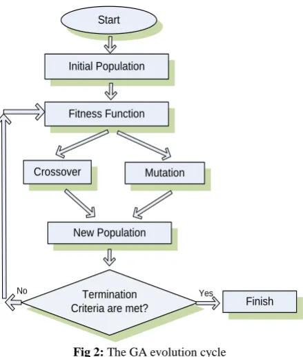
This process is continued until value of desired convergence or reaches max. generation number [21]. The GA evolution cycle was demonstrated at Fig 2.
4.
SIMULATION RESULTS
Initial Population Start
Fitness Function
Crossover Mutation
New Population
Finish
Yes No Termination
[image:3.595.58.278.69.328.2]Criteria are met?
Fig 2: The GA evolution cycle
[image:3.595.325.532.75.455.2]The simulation applications were done for same filter type and same conditions to show performance of the proposed study. The initial conditions were shown in Table 1.
Table 1. Initial conditions
Filter type BP
Passband edges Fp1 1000 Hz
Passband edges Fp2 2000 Hz
Stopband edges Fs1 500 Hz
Stopband edges Fs2 4000 Hz
Pass band ripple 1.5 dB
Stop band ripple 28 dB
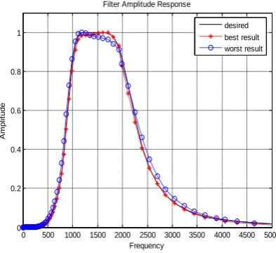
The programme results for different generation number were shown at Fig 3.
0 500 1000 1500 2000 2500 3000 3500 4000 4500 5000 0
0.2 0.4 0.6 0.8 1
Frequency
A
m
p
li
tu
d
e
Filter Amplitude Response
desired best result worst result
0 500 1000 1500 2000 2500 3000 3500 4000 4500 5000 0
0.2 0.4 0.6 0.8 1
Frequency
A
m
p
li
tu
d
e
Filter Amplitude Response
desired best result worst result
b) Generation number: 250
0 500 1000 1500 2000 2500 3000 3500 4000 4500 5000 0
0.2 0.4 0.6 0.8 1
Frequency
A
m
p
lit
u
d
e
Filter Amplitude Response
desired best result worst result
c) Generation number: 500
Fig 3: Simulation results for different generation number (a, b, c)
From the Fig 3, it is seen that GA obtained amplitude response for the generation number 250 approximately.
The programme results for different resistance values are shown in Fig 4 and data are given in Table 2.
0 500 1000 1500 2000 2500 3000 3500 4000 4500 5000 0
0.2 0.4 0.6 0.8 1
Frequency
A
m
p
li
tu
d
e
Filter Amplitude Response
desired best result worst result
[image:3.595.329.534.547.729.2]0 500 1000 1500 2000 2500 3000 3500 4000 4500 5000 0
0.2 0.4 0.6 0.8 1
Frequency
A
m
p
li
tu
d
e
Filter Amplitude Response
desired best result worst result
(b) Resistance between 1 kΩ and 9.9 kΩ
0 500 1000 1500 2000 2500 3000 3500 4000 4500 5000 0
0.2 0.4 0.6 0.8 1
Frequency
A
m
p
li
tu
d
e
Filter Amplitude Response
desired best result worst result
(c) Resistance between 10 kΩ and 99.9 kΩ
[image:4.595.68.269.76.259.2]Fig 4: Simulation results for different resistance values
Table 2. Results for different resistance values
Stage no (m)
Between 1Ω – 0.9 kΩ R1 R2 R3
Between 0.9 kΩ – 9.9 kΩ R1 R2 R3
Between 10 kΩ – 99.9 kΩ R1 R2 R3
Commands results R1=R2=R3(kΩ)
1 0.0183 0.0553 0.1015 4.4414 2.0209 1.5155 68.0069 36.4633 33.6354 22.68
2 0.1871 0.4801 0.5664 8.8508 9.0098 2.1522 16.1161 12.9521 13.0122 11.17
3 0.7324 0.3660 0.0280 9.3845 9.5990 8.7534 15.8656 55.5357 18.1917 15.92
In the circuit design implemented by taking component value equally, the design process is impossible with different component values that the user have. This problem has been removed with helping of improved method.
In Fig 4.(a), it has been found R1=0.02, R2=0.06, R3=0.1 instead of R1=R2=R3=22.7 for the first stage, R1=0.2, R2=0.5, R3=0.6 instead of R1=R2=R3=11.2 for the second stage, R1=0.7, R2=0.4, R3=0.03 instead of R1=R2=R3=15.9 for the third stage and the result close to the amplitude response that will provide desired conditions was obtained. In Fig 4.(b), it has been found R1=4.4, R2=2, R3=1.5 instead of R1=R2=R3=22.7 for the first stage, R1=8.9, R2=9, R3=2.2 instead of R1=R2=R3=11.2 for the second stage, R1=9.4,
R2=9.6, R3=8.8 instead of R1=R2=R3=15.9 for the third stage and the result close to the amplitude response that will provide desired conditions was obtained. In Fig 4.(c), it has
been found R1=68, R2=36.5, R3=33.6 instead of
R1=R2=R3=22.7 for the first stage, R1=16.1, R2=13, R3=13 instead of R1=R2=R3=11.2 for the second stage, R1=15.9, R2=55.5, R3=18.2 instead of R1=R2=R3=15.9 for the third stage and the result close to the amplitude response that will provide desired condition was obtained.
According the resistance values in between 10 kΩ and 99.9 kΩ, bandpass active filter circuit with 3 stage-6th
order was illustrated at Fig 5 for C=0.01 µF and RA=10 kΩ
+
- Op-amp
68.0
24.6
10.0
0.01
V
in+
- Op-amp
16.1
+
- Op-amp
V
out0.01
33.6
36.4
0.01
0.01
13.0
12.9
10.0
24.6
0.01
0.01
15.8
55.5
18.1
10.0
18.4
218
[image:4.595.329.526.77.257.2]10.5
[image:4.595.62.534.315.391.2] [image:4.595.69.528.569.711.2]5.
CONCLUSION
At active filter design, the using of classical calculation methods make more difficult to circuit design with different component values. In this study, the using of GA, one of the methods of the heuristic calculation, was proposed at active filter circuits that are preferred at realization of transfer function owing to natural correspondence between electronic circuit and mathematical functions. At work, selection of component value was used for different component values instead of standard series discretely works at literature and the desired amplitude response with that data was reached. In this study, the improved programme with desired initial conditions was run for circuit design that the user will define its specification and the similar amplitude responses were observed for different conditions.
At work, quadratic bandpass filter layer structure was used but, the programme can be generalized for other filter types such as lowpass, highpass and bandstop using with different circuit models.
6.
REFERENCES
[1] Thede, L. (1996). Analog and Digital Filter Design. Prentice Hall: New Jersey.
[2] Ning, Z., Kole, M., Mouthaan, T. Willings, H. (1992). Analog Circuits Design Automation for Performance. Proceedings of the 14th CICC, New York, I1 Press, 8.2.1.- 8.2.4.
[3] Jayaraman, R., Rutenbar, R.A. (1987). Floorplanning by Annealing on A Hypercube Multiprocessor. Proc. IEEE International Conference on CAD, 346-349.
[4] Wong, D.F., Liu, C.L. (1986). A New Algorithm for Floorplan Design. Processing of the 23rd ACM/IEEE Design Automation Conference, 101-107
[5] Gupta, R., Ballweber, B.M., Allstot, D.J. (2001). Design and Optimization of CMOS RF Power Amplifiers. IEEE Journal of Solid-State Circuits, 36, 166-175.
[6] Tao, L., Zhao, Y.C. (1993). Effective Heuristic Algorithms for VLSI-Circuit Partition. IEE Proceeding G: Circuits, Devices and Systems, 140, 2, 127-134.
[7] Aguirre, M.M.A., Torralba, A., Ch΄aves, J., Franquelo, L.G. (1994). Sizing of Analog Cells by means of Tabu Search Approach. In Proceedings IEEE International Symposium on Circuits and Systems, C.1, 375-378.
[8] Sadiq, S.M., Youssef, H. (1998). CMOS/BiCMOS
Mixed Design using Tabu Search. Electronics Letters, C. 34,14, 1395-1396.
[9] Sadiq, S.M., Youssef, H., Zahra, M.M. (1998). Tabu Search Based Circuit Optimization. Proceeding of the 8th Great Lakes Symposium on VLSI, 338-343.
[10]Sadiq, S.M., Youssef, H., Barada, H.R., Al-Yamani, A. (2000). A Parallel Tabu Search Algorithm for VLSI
Standard-Cell Placement. Proceeding of the IEEE International Symposium on Circuits and Systems ISCAS 2000, C.2, 581-584.
[11]Lodha, S.K., Bhatia, D. (1998). Bipartitioning Circuits using Tabu Search. Proceedings of Eleventh Annual IEEE International Conference ASIC, 223-227.
[12]Kuntz, P., Layzell, P., Snyers, D. (1997). A Colony of Ant-like Agents for Partitioning in VLSI Technology. In: Proc. 4th International Conference on Artificial Life (ECAL97), P. Husbands and I. Harvey (eds.), MIT Press.
[13]Kalinli, A. (2003). Component Value Selection for Active Filters Using Ant Colony Algorithm. Dokuz Eylul University Journal of Science and Engineering, 5(3), 41-53.
[14]Kruiskamp, W., Leenaerts, D. (1995). DARWIN:CMOS
Opamp Synthesis by means of A Genetic Algorithm. Proceeding of the 32nd Design Automation Conference,
New York, Association for Computing Machinery, 433-438.
[15]Paulino, N.F., Goes, J.C., Steiger, A. (2001). Design Methodology for Optimization of Analog Building Blocks using Genetic Algorithms. The 2001 IEEE International Conference on Circuits and Systems, C.5, 435-438.
[16]Grimbleby, J.B. (2000). Automatic Analogue Circuit Synthesis using Genetic Algorithms. IEE Proc. Circuits Devices Syst., C.147, No.6, 319-323.
[17]Horrocks, D.H., Khalifa, Y.M.A. (1994). Genetically Derived Filters Circuits using Preferred Value Components. Proc. of IEE colloq. on Linear Analogue Circuits and Systems, Oxford UK.
[18]Horrocks, D.H., Spittle, M.C. (1995). Component Value Selection for Active Filters using Genetic Algorithms. C2. 553-556.
[19]Horrocks, D.H., Khalifa, Y.M.A. (1995). Genetically Evolved FDNR and Leap-Frog Active Filters using
Preferred Component Values. Proc. European
Conference on Circuits Theory and Design, Turkey, 359-362.
[20]Horrocks, D.H., Khalifa, Y.M.A. (1996). Genetic Algorithm Design of Electronic Analogue Circuits Including Parasitic Effects. Proc. First On-Line
Workshop on Soft Computing (WSC1),Nagoya
University, Japan, 71-78.