Simulations and Analysis of Nano Scale
Porous Silicon Structures for Optical Sensor
Applications
P. N. Patel
Electronics Engg. Deptt.
S. V. National Institute of Technology, Surat
Vivekanand Mishra,
SMIEEEElectronics Engg. Deptt.
S. V. National Institute of Technology, Surat
ABSTRACT
Recently, Porous Silicon (PS) is emerged as novel and unique material as a stable nano scale optical sensor device. In this work, one dimensional (1D) Photonic Bandgap (PBG) structures such as single layer (SL), Distributed Bragg Reflector (DBR) and Microcavity (MC) using PS material are suggested as optical sensor applications. Design and simulations are relying on the Bruggeman’s Effective Medium Approximation (BEMA) and the Transfer Matrix Method (TMM) to predict the optical properties of 1D-PSPBG sensor device structures. By analyzing the reflectance spectra, wavelength shift (Δλ) has been obtained, which showed good linear relationship with refractive index of the void. Sensitivity analysis showed that MC structure performs best as 1D-PSPBG optical sensor device due to its structural and optical properties. The results reported here are useful for the design and prediction of the response of optical sensor devices using 1D-PSPBG structures.
Keywords
Porous silicon; Photonic Band gap Structures; Bruggeman’s Effective Medium Approximation; simulation of Optical Sensor Device.
1.
INTRODUCTION
1D-PBG structures are periodic dielectric structures that control the propagation of electromagnetic wave through the photonic crystals [1-4]. In past years, 1D-PBG structures attracted lot of attention of scientist and researchers, due to their enormous advantages and applications in optoelectronic devices, instrumentation and sensors [5-8]. PS is a two phase composite structure, being a mixture of air and the silicon solid phase containing the silicon network with silicon walls and pores [9]. In recent years, PS is emerged as a promising 1D-PBG structure in nano scale optical sensor device due to tremendous advantages. Its large surface area within a small volume, silicon based easy fabrication, controllable pore sizes, convenient surface chemistry and ability to modulate its refractive index as a function of depth makes it suitable for many real world applications [10]. In the porous structure, PS contains large number of pores which is useful as a host for the detection of analytes because its optical properties [11] are highly sensitive to the presence of chemical and biological species inside the pores. All these features make 1D-PSPBG structures suitable for many emerging optical sensor applications.
Till date number of publications on fabrication, characterizations and applications are reported [12-15] using PS structure. But still there is lake of systematic theoretical analysis. In this work, numerical simulations and analysis of 1D-PSPBG sensor device structures has been done. In section
2, theory of optical sensing using PS structure based on the reflectance spectra is described. Section 3 deals with the detailed results and discussion of the simulations for different structures. Finally, this theoretical work leads to set up the optimized conditions based on the wavelength shift and sensitivity analysis of different structures.
2.
THEORY
Principle of interferometric optical transduction is used in PS based optical sensing [16]. The reflectance spectrum is determined by the effective optical thickness of the entire structure. The optical thickness is defined as the product of the refractive index and the physical thickness of the structure. The peak positions of the fringes are determined by the following Eq. 1:
where, m = integer, λ = peak wavelength, n = effective refractive index of the layer, h = thickness of the layer.
For the multilayer PS structures such as DBR and MC consists of a stack of thin PS layers of alternating high refractive index layers and low refractive index layers. In such a case, the interferometric Fabry-Perot relation of Eq. 1 becomes [17]:
where, λ0 = Photonic resonance wavelength, nL and hL =
Refractive index and the thickness of the low index layer, respectively, nHand hH = Refractive index and the thickness
of the high index layer, respectively.
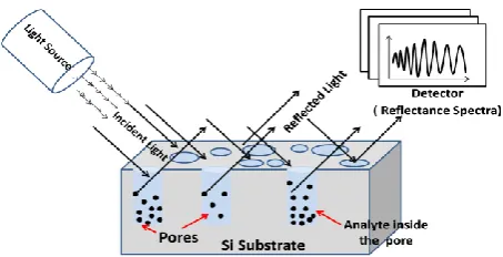
As shown in Fig. 1, light reflected from the top interface (air-PS) and the bottom interface (PS-Si substrate) interfere with each other and form the typical Fabry-Perot fringes in the reflectance spectrum. When pores are not infiltrated (i.e. nvoid
= 1= air) then the refractive index of PS is nps and the
wavelength in the reflectance spectrum is . When the pores are infiltrated with an analyte (i.e. nvoid > 1) like
chemical, biochemical or biological objects, the effective refractive index of the PS layer increases from nps to nps + Δn
and hence the resultant wavelength in the reflectance spectra shifts from to a longer wavelength . Where, = Reference wavelength for = Air =1,
= Shifted wavelength for > 1 (when analyte is
Fig 1: Schematic drawing of single layer PS interferometric optical sensor device
Optical properties of 1D-PSPBG sensor device structure directly depend on refractive index (n), thickness (h) and the porosity (P) of the layers. These parameters are the base of the simulations and analysis of 1D-PSPBG structures. Refractive index of the 1D-PSPBG layers with the porosity is related by BEMA model [18]. This approximation is acceptable because the size of the pore is much smaller than the wavelengths of incidence light in the near UV-VIS-IR regions. In this range, the electromagnetic radiation does not distinguish between silicon and void, and it is possible to treat the PS as a homogeneous medium.
If not exposed to the analyte, PS can be simplified as a uniform mixture of silicon and air. Thus, one can calculate the effective refractive index of the PS from Eq. 3 and 5.
where, P = Porosity of the PS, = dielectric constant of silicon, = dielectric constant of PS, = dielectric constant of the medium inside the pores (air/analyte), = refractive index of silicon, = refractive index of PS, = refractive index of the medium inside the pores (air/analyte).
Wave transmission in a 1D-PSPBG structure is realized based on TMM [6, 19].
3.
SIMULATIONS, RESULTS AND
DISCUSSION
To study the sensing performance of the different 1D-PSPBG structures, critical parameters such as physical thickness and refractive index (or porosity) are considered. The schematic diagram of 1D-PSPBG structures such as single layer, DBR and MC are shown in Fig. 2 (a), (b) and (c), respectively.
Design of single layer 1D-PSPBG structure is simple as it is a two phase composite, being a mixture of air and the silicon solid phase. It can be designed using Eq. 1. As shown in Fig. 2 (b), DBR is periodic multilayer structure formed by the periodic repetition of two layers with different refractive indices and thicknesses according to Eq. 6.
where, n1 and h1 are the refractive index and the thickness of
the low refractive index layer, while n2 and h2 are the
refractive index and the thickness of the high refractive index layer. When this condition, called the ‘Bragg condition’, is fulfilled, the light at wavelengths in the range of the photonic band gap of the crystal is reflected giving photonic stop band of the Bragg reflector centered at λ0. The design schematic
diagram of MC is shown in Fig. 2 (c). To obtain the desired MC, the optical thickness of the cavity layer, situated between the two DBRs, is half the wavelength for which the structure is designed according to Eq. 7.
where, nc and hc being the refractive index and the thickness
of the defect or cavity layer.
All the simulations are done for the normal incidence of the light. Refractive index of ambient medium n0, and substrate is
1.0 and 3.4, respectively, while the wavelength range of analysis is 400-1200 nm. Also our basic aim is to observe the wavelength shift in the reflectance spectra hence we have neglect the absorption effects.The critical design parameters for simulation are: porosity (%), refractive indices of the layers and the thickness of layers. Refractive index is related with porosity by BEMA theory as per Eq. 5. The porosity of the low refractive index, high refractive index and the microcavity layers are chosen as 56.5%, 25% and 64%, respectively as it is suitable with fabrications. Corresponding values of refractive indices of layers n1, n2 and nc had been
calculated as 2.0, 2.95 and 1.75 which is also suitable with fabrications. DBR and MC structures are designed for the resonance wavelength of 800 nm; hence the corresponding layer thicknesses h1, h2 and hc are calculated from the Eq. 6
and 7, which are 100 nm, 67.77 nm and 227.87 nm, respectively. DBR is realized by the twenty repetitions of low and high refractive indices. Microcavity is realized by the two symmetric DBRs of six repetitions with cavity layer in the center.
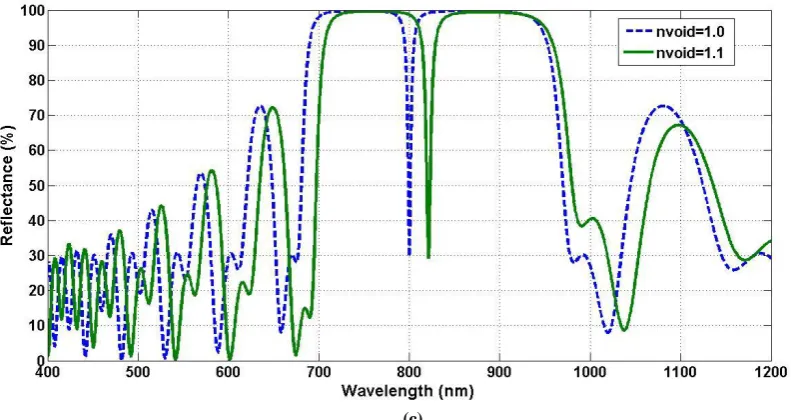
Based on the above values, simulation is done for the nvoid =
(a) (b) (c) Fig 2: Schematic Diagram of (a) Single Layer, (b) DBR and (c) MC Structure
(a)
(c)
Fig 3: Reflectance Spectra of (a) single layer, (b) DBR and (c) MC Structures
As shown in the Fig. 3 (a), fringes in the reflectance spectrum can be observed for the single layer structure, because it is a two phase composite mixture of air and the silicon solid phase. It is remarkable to observe the photonic resonance centered at near 800 in the reflectance spectrum of DBR and MC structures respectively. Also, it is clearly visible in the Fig. 3 (a), (b) and (c) that as the refractive index of the void is changed from 1.0 to 1.1, the remarkable shift in the wavelength is observed in the reflectance spectrum of different structures. One can observe in the Fig. 3 (a) that, in single layer structure there is lake of any benchmark or reference wavelength for the accurate measurement of the wavelength shift, while in the case of DBR structure, the center wavelength can be used as the reference wavelength (Fig. 3 (b)). In the case of MC structure, sharp photonic resonance that appears as a dip in the reflectance spectrum which is highly sensitive to finite changes in the refractive index of void (Fig. 3 (c)). These simulations are done for the different values of the refractive index of voids for all the structures and the wavelength shift is measured and listed in the Table 1.
Table1. Effect of nvoid on the Δλ
nvoid Δλ (nm)
Single Layer DBR MC
1.0 0.00 0.00 0.00
1.1 1.02 15.12 21.15
1.2 1.57 30.68 41.38
1.3 2.57 44.78 59.62
1.4 4.18 60.82 76.79
1.5 5.49 74.41 93.96
1.6 7.09 90.96 109.75
1.7 8.80 105.54 124.86
1.8 10.66 121.08 139.29
1.9 12.28 136.66 153.02
As shown in the Table 1, the standard variations in the wavelength shift of the multilayer DBR and MC PSPBG structures is consistently higher than those of the single layer structure. This is due to the different structural properties of these structures. Due to multilayer nature of these structures, effective refractive index of the bare structure (without any
analyte) is higher than the single layer structure according to Eq. 2 and hence the optical thickness are much larger than that of single layer structure. Also, the wavelength shift depends on the refractive index of the void as per Eq. 1. When the refractive index of void is high, large variations in the wavelength shift in the reflectance spectra is observed; correspondingly, when the refractive index of the void is low, small variations in the reflectance spectra is observed in each case of 1D-PSPBG structure.
Sensitivity is one of the most important issues to evaluate the performance of the sensor device. In this case, the response of the sensor device is evaluated throughout the change of the wavelength shift ( ) in the reflectance spectrum for change in the refractive index ( ). Sensitivity (S) is defined as:
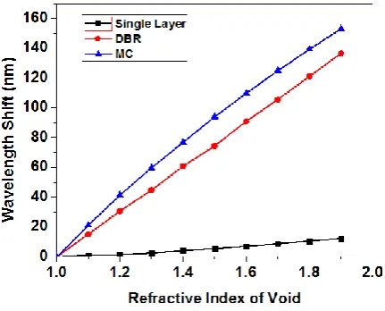
This parameter shows to be a good indicator for sensing measurement in the 1D-PSPBG sensing devices. The relationship between refractive index of the void and the wavelength shift is plotted in Fig. 4 from the data listed in Table 1. Calculated sensitivity is 14.07, 151.93 and 164.84 for the single layer, DBR and MC sensor device structures respectively.
[image:4.595.91.487.83.293.2]reflectance spectrum of MC due to sharp resonance peak in the reflectance spectra.
Fig 4: Refractive Index of Void vs. Wavelength Shift
4.
CONCLUSIONS
To conclude, one dimensional porous silicon based photonic bandgap structures are suggested as optical sensor devices. Simulation program was developed and investigations were done for different 1D-PSPBG sensor device structures. Simulation parameters were chosen as per the suitability for fabrications of these structures. It was observed that slight refractive index change in refractive index of void causes a sufficiently large wavelength shift, which can be very easily detected by monitoring reflectance spectrum, with the help of existing sophisticated optical spectroscopy. Higher wavelength shift was observed in the case of higher refractive index of void for all the suggested sensor devices. The reflectance spectra of the different 1D-PSPBG structures showed good linear relation for the wavelength shift with respect to change in the refractive index of void. Highest wavelength shift, measurement accuracy and the sensitivity was observed for the MC structure due to its structural and optical properties. These 1D-PSPBG sensor devices found potential applications in chemical, biochemical and biological analyte sensing elements.
5.
ACKNOWLEDGMENT
This work was supported by the grant from Defence Research and Development Organization (DRDO), Govt. of India.
6.
REFERENCES
[1] Yablonovitch E., “Inhibited spontaneous emission in solid state physics and electronics,” Phys. Rev. Lett., Vol. 58, pp. 2059-2062, 1987.
[2] Yablonovitch E., “Photonic band gap structures,” Journal of Optical Society of America B, Vol. 10, pp. 283-295, 1993.
[3] R H Lipson and C Lu, “Photonic crystals: a unique partnership between light and matter”, Eur. J. Phys. Vol. 30, pp. 33, 2009.
[4] A. Banerjee, “Enhanced Refractometric Optical Sensing By Using One-Dimensional Ternary Photonic Crystals”, Progress In Electromagnetics Research, PIER, Vol. 89, pp. 11-22, 2009.
[5] Hopman, W. C. L.,P . Pottier, D. Yudistira, J. V. Lith, P. V. Lambeck, R. M. De, L. Rue,A. Driessen, H. J. W. M. Hoekstra and R. M. de Ridder, “Quasi-one-dimensional photonic crystal as a compact building-block for refractometric optical sensors,” IEEE J. Selected Topics in Quantum Electronics, Vol. 11, No.1, pp.11-16, 2005. [6] Sunita P. Ugale, V. Mishra, “Modeling and
characterization of fiber Bragg grating for maximum reflectivity”, Optik, Vol. 122, pp. 1990-1993, 2011.
[7] Luca De Stefano, Ivo Rendina, Luigi Moretti, Stefania Tundo, and Andrea Mario Rossi, “Smart Optical Sensors for Chemical Substances Based on Porous Silicon Technology”, Applied Optics, Vol. 43, Issue 1, pp. 167-172, 2004.
[8] Victor S. Y. Lin, Kianoush Motesharei, Keiki-Pua S. Dancil, Michael J. Sailor, M. Reza Ghadiri, , “A Porous Silicon-Based Optical Interferometric Biosensor”, Science, Vol. 278, no. 5339, pp. 840-843, 1997.
[9] Liegh Canham (ed.), “Properties of Porous Silicon” INSPEC, London, 1st Ed., 1997.
[10] A. G. Cullis, L. T. Canham and P. D. J. Calcott, “The Structural And Luminescence Properties Of Porous Silicon”, J. Appl. Physics, Vol. 82, No. 3, August 1997.
[11] W. Theiss, “Optical properties of porous silicon”, Surf. Sci. Rep. 29, pp. 91-192, 1997.
[12] P. N. Patel, V. Mishra, A. K. Panchal, “Synthesis and characterization of nano scale porous silicon photonic crystals for optical device and sensing applications”, Journal of Optoelectronics and Biomedical Materials, vol. 4, issue 1, pp. 19-28, 2012.
[13] P. N. Patel, V. Mishra, A. K. Panchal, “Theoretical and Experimental Study of Nano Porous Silicon Photonic Microcavity Optical Sensor Devices”, Adv. Nat. Sci.: Nanosci. Nanotechnol. vol. 3, 2012.
[14] P. N. Patel, V. Mishra, A. K. Panchal, N. H. Maniya, “Realization of porous silicon distributed Bragg reflector for optical sensing applications”, Sensors & Transducers Journal, Vol. 139, Issue 4, pp. 79-86, 2012.
[15] P. N. Patel, V. Mishra, A. K. Panchal, “Nano porous silicon microcavity optical biosensor device for glucose detection”, Digest Journal of Nanomaterials and Biostructures, vol. 7, no. 3, pp. 973-982, 2012.
[16] Hee-Kyung Min, Ho-Sik Yang, Sung M. Cho., “Extremely Sensitive Optical Sensing Of Ethanol Using Porous Silicon”, Sensors and Actuators B, vol. 67, pp. 199-202, 2000.
[17] Han-Jung Kim, Young-You Kim, Ki-Won Lee, Horchhong Cheng and Dong Han Ha, Physica B, 406, 1536 (2011).
[18] M. Khardani, “Bruggeman Effective Medium Approach for Modeling Optical Properties of Porous Silicon: Comparison with Experiment,” phys. stat. sol. (c) 4, No. 6, pp. 1986-1990, 2007.