Virginia Commonwealth University Virginia Commonwealth University
VCU Scholars Compass
VCU Scholars Compass
Theses and Dissertations Graduate School
2017
IMPROVING THE PERFORMANCE AND TIME-PREDICTABILITY OF
IMPROVING THE PERFORMANCE AND TIME-PREDICTABILITY OF
GPUs
GPUs
Yijie HuangfuFollow this and additional works at: https://scholarscompass.vcu.edu/etd
Part of the Computer and Systems Architecture Commons
© The Author
Downloaded from Downloaded from
https://scholarscompass.vcu.edu/etd/4930
This Dissertation is brought to you for free and open access by the Graduate School at VCU Scholars Compass. It has been accepted for inclusion in Theses and Dissertations by an authorized administrator of VCU Scholars
c
Yijie Huangfu, May 2017 All Rights Reserved.
IMPROVING THE PERFORMANCE AND TIME-PREDICTABILITY OF GPUS
A dissertation submitted in partial fulfillment of the requirements for the degree of Doctor of Philosophy at Virginia Commonwealth University.
by
YIJIE HUANGFU, PH.D. VIRGINIA COMMONWEALTH UNIVERSITY, MAY 2017
Director: Wei Zhang, Ph.D.
Professor, Department of Electrical and Computer Engineering
Virginia Commonwewalth University Richmond, Virginia
Acknowledgements
I thank my advisor, Prof. Wei Zhang. I am grateful for the opportunity of work-ing with Prof. Zhang in this Ph.D. program, where I received excellent trainwork-ing and insightful guidance and feedback from him. With his diligence and preciseness, Prof. Zhang sets up a model for young academics to follow to succeed. I also appreciate Prof. Zhang’s supportive attitude in encouraging me to explore research ideas and career opportunities.
Dr. Carl Elks, Dr. Preetam Ghosh, Dr. Weijun Xiao and Dr. Qiong Zhang, who also nicely serve on my committee, are appreciated for their highly suggestive feedback and comments to my research plan proposal. I also thank their efforts and patience in accommodating my proposal and dissertation defense dates to their tight schedules.
I thank my friends Elaine and Bob Metcalf, Susie and Bud Whitehouse, Kate and Lex Strickland, Jan and Jim Fiorelli, Geoffrey and Eunice Chan, Kun Tang, Tao Lyu and Qianbin Xia for being a huge and wonderful part in my life at Richmond. It is such a blessing to know them and to have them as friends.
I thank my parents for giving me life and the abilities and educations, with which I can survive and thrive. I thank my parents in law for their unfailing supports, without which I could not finish my Ph.D. program. I thank my daughter Claire for bring joy, hope and noisy peace to the family. Specially, I thank my wife Xiaochen, who is always supportive and encouraging and is forever the source of my energy for pursuing excellence.
TABLE OF CONTENTS
Chapter Page
Acknowledgements . . . ii
Table of Contents . . . iii
Abstract . . . . 1 Introduction . . . 1
1.1 Background . . . 1
1.2 GPU L1 Data Cache Bypassing . . . 3
1.3 GPU L1 Data Cache Access Reordering . . . 3
1.4 WCET Timing Model for GPU Kernels . . . 4
1.5 WCET Analysis of Shared Data LLC in integrated CPU-GPU Architecture . . . 4
1.6 Dissertation Organization . . . 5
2 GPU Architecture and GPGPU Programming Model . . . 6
2.1 GPU Architecture . . . 6
2.2 GPGPU Programming Model . . . 7
3 Profiling-Based GPU L1 Data Cache Bypassing . . . 9
3.1 Introduction . . . 9
3.2 Related Work . . . 10
3.3 Profiling-Based GPU L1 data Cache Bypassing Method . . . 11
3.3.1 Global Memory Access Utilization . . . 11
3.3.2 Global Memory Reuse Time . . . 13
3.3.3 Heuristic for GPU Cache Bypassing . . . 14
3.4 Evaluation Results . . . 16
4 Warp-Based Load/Store Reordering for Better Time-Predictability in GPU L1 Data Cache . . . 19
4.1 Introduction . . . 19
4.2 Related Work . . . 20
4.3.1 Dynamic Warp Scheduling . . . 21
4.3.2 Out-of-Order Execution . . . 21
4.3.3 Independent Execution Among Warps . . . 22
4.4 GPU L1 Data Cache Access Reordering Framework . . . 23
4.4.1 Challenges of GPU Execution on Cache Timing Analysis . . 23
4.4.2 Issues of Regulating the Warp Scheduling Orders . . . 24
4.4.3 The Load/Store Reordering Framework . . . 24
4.4.4 Compiler-Based Kernel Analyzer . . . 25
4.4.5 Architectural Extension for Warp-Based Load/Store Reordering 29 4.4.6 GPU L1 Data Cache Miss Rate Estimation . . . 34
4.4.6.1 Limitation of the GPU L1 Data Cache Timing Analyzer 36 4.5 Evaluation Results . . . 37
4.5.1 Performance Results . . . 37
4.5.2 GPU L1 Data Cache Miss Rate Estimation Results . . . 38
5 Timing Model for Static WCET Analysis of GPU Kernels . . . 41
5.1 Introduction . . . 41
5.2 Related Work . . . 42
5.3 GPU WCET Analysis with Predictable Warp Scheduling . . . 43
5.3.1 Pure Round-Robin Scheduler Timing Model . . . 43
5.3.2 Code Segment Issuing and Execution Latency Timing Models 46 5.3.3 Static GPU Kernel Analyzer . . . 50
5.3.3.1 Warp Scheduling Order . . . 51
5.3.3.2 Number of Coalesced Memory Accesses . . . 51
5.3.3.3 Number of Competing SMs . . . 53
5.4 Evaluation Results . . . 57
6 Static WCET Analysis on Last Level Data Cache in Integrated CPU-GPU Architecture . . . 61
6.1 Introduction . . . 61
6.2 Related Work . . . 62
6.3 Reuse Distance . . . 63
6.4 Shared LLC Analysis . . . 64
6.4.1 The Integrated CPU-GPU Architecture Under Analysis . . . 64
6.4.2 Simple Shared Data LLC Analysis Method . . . 64
6.4.3 Access Interval Based Shared Data LLC Analysis Method . . 67
6.5 WCET Analysis of GPU Kernels with Shared Data LLC Esti-mation Results . . . 71
6.6 Evaluation Results . . . 72 6.6.1 Experimental Methodology . . . 72 6.6.1.1 Simulator . . . 72 6.6.1.2 Benchmarks . . . 73 6.6.1.3 Assumptions . . . 74 6.6.2 Experiment Results . . . 75
6.6.2.1 Shared Data LLC Miss Rate Estimation Results . . . 75
6.6.2.2 WCET Estimation Results of GPU Kernels . . . 77
7 Conclusions . . . 80
7.1 Profiling-Based GPU L1 Data Cache Bypassing . . . 80
7.2 Warp-Based Load/Store Reordering for Time-Predictability Im-provement . . . 81
7.3 Static WCET Analysis Timing Model for GPUs . . . 82
7.4 Static WCET Analysis on Shared Data LLC in CPU-GPU Ar-chitectures . . . 82
7.5 Future Work . . . 83
References . . . 84
Abstract
IMPROVING THE PERFORMANCE AND TIME-PREDICTABILITY OF GPUs
By Yijie Huangfu, Ph.D.
A dissertation submitted in partial fulfillment of the requirements for the degree of Doctor of Philosophy at Virginia Commonwealth University.
Virginia Commonwealth University, 2017
Major Director: Wei Zhang, Professor, Electrical and Computer Engineering
Graphic Processing Units (GPUs) are originally mainly designed to accelerate graphic applications. Now the capability of GPUs to accelerate applications that can be parallelized into a massive number of threads makes GPUs the ideal accelerator for boosting the performance of such kind of general-purpose applications. Meanwhile it is also very promising to apply GPUs to embedded and real-time applications as well, where high throughput and intensive computation are also needed.
However, due to the different architecture and programming model of GPUs, how to fully utilize the advanced architectural features of GPUs to boost the performance and how to analyze the worst-case execution time (WCET) of GPU applications are the problems that need to be addressed before exploiting GPUs further in embedded and real-time applications. We propose to apply both architectural modification and static analysis methods to address these problems. First, we propose to study the GPU cache behavior and use bypassing to reduce unnecessary memory traffic and to improve the performance. The results show that the proposed bypassing method
can reduce the global memory traffic by about 22% and improve the performance by about 13% on average. Second, we propose a cache access reordering framework based on both architectural extension and static analysis to improve the predictabil-ity of GPU L1 data caches. The evaluation results show that the proposed method can provide good predictability in GPU L1 data caches, while allowing the dynamic warp scheduling for good performance. Third, based on the analysis of the architec-ture and dynamic behavior of GPUs, we propose a WCET timing model based on a predictable warp scheduling policy to enable the WCET estimation on GPUs. The experimental results show that the proposed WCET analyzer can effectively provide WCET estimations for both soft and hard real-time application purposes. Last, we propose to analyze the shared Last Level Cache (LLC) in integrated CPU-GPU ar-chitectures and to integrate the analysis of the shared LLC into the WCET analysis of the GPU kernels in such systems. The results show that the proposed shared data LLC analysis method can improve the accuracy of the shared LLC miss rate estima-tions, which can further improve the WCET estimations of the GPU kernels.
CHAPTER 1
INTRODUCTION
1.1 Background
In the past decade or so, Graphics Processing Units (GPUs), originally designed to accelerate graphical computation, have rapidly become a popular platform for high-performance parallel computing. Modern GPUs can support massive parallel computing with thousands of cores and extremely high-bandwidth external memory systems. The single-instruction multiple-thread (SIMT) programming model used by GPUs well matches the underlying computing patterns of many high-performance embedded applications, including imaging, audio, video, military, and medical appli-cations [1]. At the same time, GPUs are increasingly used in System-on-Chips (SoCs) for mobile devices, for example ARM’s Mali graphics processor [2], the NVIDIA Tegra[3] and the DRIVE PX platform [4].
GPUs can also provide considerable benefits to a variety of real-time applications that demand high throughput and energy efficiency. In particular, GPUs are promis-ing for many computation-intensive hard real-time and safety-critical applications such as medical data processing [5], autonomous auto navigation [6], vision-based aircraft controls [7] and human pose recognition [8]. All these applications need to meet strict deadlines and require high system throughput, making GPUs the ideal potential computing engines for them.
There are efforts made to explore the performance and energy benefits of the heterogeneous CPU-GPU architectures. For instance, the management method in [9] employs a unified Dynamic Voltage Frequency Scaling (DVFS) approach to further
reduce the power consumption for 3D mobile games. Studies have also been done on real-time image processing in different types of applications based on the CPU-GPU architecture[10][11][12]. Besides the real-time image processing field, moreover, the CPU-GPU architecture is more and more used in other real-time applications, e.g. the NVIDIA PX 2 self-driving car computing platform[4] using the Tegra[3] chips. And, with the development of the general purpose GPU programming model and the CPU-GPU architectures, it is expected that such architectures will be widely used in all kinds of different real-time applications, e.g. computer vision, automation control and robotics.
However, many GPU architecture features designed for improving the average-case performance are harmful to the time-predictability feature of the system. There-fore, before exploiting the computing power of GPUs in these applications, the im-pacts of these advanced GPU architecture features in time-predictability and perfor-mance need to be analyzed and studied accordingly. One example is the usage of cache memories. In CPUs, cache memories help to reduce the speed gap between the processor cores and the main memory, by exploiting the spacial and temporal localities. GPU applications, nevertheless, are different in spacial and temporal lo-calities, which leads to the first problem of how to better utilize the cache memory in GPUs. According to the time-predictability of GPUs, the advanced architecture features, such as dynamic scheduling and out-of-order execution, make it very hard, if not impossible, to estimate the WCET of GPU applications, since at run-time there are usually thousands of warps scheduled and executed dynamically. Furthermore, the trend of building and utilizing the integrated CPU-GPU architectures raises the problem of how to model the behavior of the shared resources in such architectures, e.g., the shared Last Level Cache (LLC), so that the behavior of the whole chip in the worst case can be better modeled.
1.2 GPU L1 Data Cache Bypassing
The first topic is about using cache bypassing to study the impact of the GPU L1 data cache on the performance and finding a way to use the GPU L1 data cache more effectively. We comparatively evaluate the GPU performance without and with the cache memory. We find that unlike CPU caches, GPU applications tend to exhibit low temporal and/or spatial locality in the L1 data cache. On average, the GPU with the L1 data cache actually leads to worse performance than the one without the L1 data cache. However, this does not necessarily imply that caches should not be used for real-time GPU computing. By examining the GPU application behavior and architectural features, we propose to use GPU L1 data cache bypassing methods to filter out the GPU cache accesses that are detrimental to performance, so that the cache can be used in a more effective way.[13]
1.3 GPU L1 Data Cache Access Reordering
Secondly, the dynamic warp scheduling operations in GPUs can benefit the average-case performance of general-purpose GPU (GPGPU) applications. But such a kind of dynamic behaviors is hard to be analyzed statically. Therefore, we propose a warp-based load/store reordering framework that is based on collaborative static analysis and architectural extensions in GPUs to improve the predictability of the GPU L1 data caches. The proposed framework supports dynamic warp scheduling while reordering the load/store instructions to enable safe and accurate timing anal-ysis for L1 GPU data caches. As a result, the predictability is improved without putting constraints on the dynamic warp scheduling behaviors, which helps to keep good average-case performance.[14]
1.4 WCET Timing Model for GPU Kernels
The third effort is to build a timing model and static analyzer for the purpose of GPU WCET analysis and estimation. We proposed to employ a predictable pure round-robin scheduling policy, based on which a timing model is built for GPGPU kernels. With this timing model, a static analyzer is built to analyze the assembly codes of the GPGPU kernels and to give their WCET estimations. Building such a kind of low-level timing model of a processor architecture requires detailed docu-mentation of the processor, which is usually unavailable for GPUs. Furthermore, the proposed methods involve changes in the architecture. Therefore, the detailed and configurable GPU simulatorGPGPU-Sim [15] is used to implement and evaluate the proposed model and analyzer.
1.5 WCET Analysis of Shared Data LLC in integrated CPU-GPU
Ar-chitecture
The last work is to improve the time-predictability of the integrated CPU-GPU architectures. Specifically, the focus in this work is the shared Last Level Cache (LLC). The method of Access Interval regulations is used to improve the time-predictability of the shared data LLC, according to the cache miss rate estimations. The improved miss rate estimations are then integrated into the WCET timing model for better WCET estimations of GPU kernels. Thegem5-gpu[16] simulator is used to implement the integrated architecture with shared LLC and to evaluate the impact of the shared LLC in such systems.
1.6 Dissertation Organization
The rest of the dissertation is organized as follows. Chapter 2 briefly introduces the background information about the GPU architecture and GPGPU programming model. In Chapter 3, the profiling-based GPU L1 data cache bypassing is present to illustrate how the GPU L1 data caches can be used in a more effective way. Chapter 4 talks about a reordering framework, which is based on both architectural extensions and static analysis, and how this framework can improve the predictability of the GPU L1 data cache. A timing model for WCET analysis of GPU kernels that is based on a predictable warp scheduling policy is introduced in Chapter 5, after which a static WCET analysis technique for the shared data LLC in the integrated CPU-GPU architecture is discussed in Chapter 6. In Chapter 7, the conclusions are made.
CHAPTER 2
GPU ARCHITECTURE AND GPGPU PROGRAMMING MODEL
2.1 GPU Architecture
Fig. 1 shows the basic architecture of a NVIDIA GPU1, which has a certain number of Streaming Multiprocessors (SMs), e.g., 16 SMs in Fermi architecture[17]. All the SMs share the L2 cache, through which they access the DRAM global memory. Other parts, like the interface to host CPUs, are not included in Fig. 1.
L2 Cache . . . . . . SM SM SM SM SM SM . . . . . . SM SM SM SM SM SM D R A M D R A M D R A M D R A M
Fig. 1. GPU Architecture[17]
Fig. 2 shows the architecture of an SM, which contains a group of Shader Pro-cessors (SPs, also called CUDA processor or CUDA core). Each SP has the pipelined integer arithmetic logic unit and floating point unit, which execute the normal arith-metic instructions, while the Special Function Units (SFUs) execute the transcenden-tal instruction, such as sin, square root, etc. Besides the computing functional units, there are several L1 caches for instruction, data, texture data and constants. The register file contains a huge number of registers shared by all the SPs and SFUs, while the warp scheduler and dispatching unit choose among the active warps and collect
the operands needed and send the warp to execution. Instruction Cache
Constant
Cache TextureCache L1 DataCache
. . . Dispatching Unit Registers File SFU . . . LD/ST . . . SP SP SP SP SP SP SP SP SFU LD/ST Warp Scheduler Fig. 2. SM Architecture[17]
2.2 GPGPU Programming Model
With the support of a massive number of cores, GPUs use the SIMT execution model to allow a big number of threads to execute in parallel. A GPGPU pro-gram, which is also called a GPU kernel, can be written in either CUDA C[18] or OpenCL[19]. A GPU kernel is configured and launched by a host CPU. Through the configuration of the kernel, the host CPU tells the GPU how many threads there are in the execution of the kernel and what the hierarchy of the threads is like. The hierarchy of a kernel has two levels; the dimensions in kernel grid (how many kernel blocks there are in a kernel grid) and in kernel block (how many threads there are in a kernel block). For example, the kernel in Fig. 3 has64 (2×4×8) kernel blocks in the kernel grid and 512 (32×16×1) threads in one kernel block.
The kernel code describes the function and behavior of a single thread, based on the position of this thread in the hierarchy of the kernel, e.g., thread and block IDs.
dim3 grdDim( 2, 4, 8);
dim3 blkDim(32,16, 1);
Kernel<<<grdDim, blkDim>>>(...);
Fig. 3. GPU Kernel Configuration Example
The most common way is to use the thread and block IDs to calculate the indices, which each thread uses to access a certain array, so that the threads work on different parts of the data in parallel. In the execution of a GPU kernel, a kernel block is assigned to an SM and stays there until finishing its execution. 32 threads in a kernel block are grouped together as the basic scheduling and execution unit, which is called a warp. The threads in the same warp execute the same instruction together in the SIMT model. Therefore, a GPU kernel instruction is also called a warp instruction.
CHAPTER 3
PROFILING-BASED GPU L1 DATA CACHE BYPASSING
3.1 Introduction
To exploit the localities in GPGPU applications and boost the average-case per-formance, both the L1 data cache and the unified L2 cache are included in modern GPUs. Although the cache memory can effectively hide the access latency for data with good temporal and/or spatial locality for both CPUs and GPUs, GPGPU plications may exhibit divergent memory access patterns from traditional CPU ap-plications. Moreover, the recent study shows that GPU caches have counter-intuitive performance trade-offs [20]. Therefore, it is important to explore the techniques to use the on-chip cache memories effectively to boost GPU performance and/or energy efficiency. In particular, for embedded and mobile GPU applications, it is also cru-cial to develop cost-effective optimization methods for improving performance and/or energy efficiency.
To address this problem, we comparatively evaluate the GPU performance with-out and with the cache memory. As the first step toward studying time predictability of GPU caches, we focus on the L1 data cache. we find that unlike CPU caches, GPU applications tend to exhibit low temporal and spatial locality in the L1 data cache. On average, the GPU with the L1 data cache actually leads to worse performance than the one without the L1 data cache. However, this does not necessarily imply that caches should not be used for real-time GPU computing.
By examining the GPU application behavior and architectural features, we pro-pose a profiling-based cache bypassing method to filter out the GPU cache accesses
that are detrimental to performance. The evaluation results show that the cache bypassing method improves the performance adequately as compared to the GPU without using the cache, because the rest of GPU memory accesses with good tem-poral and spatial locality can still efficiently exploit the L1 data cache. Therefore, employing the L1 data cache can still benefit real-time GPU applications in terms of the average-case performance; however, time-predictable architecture or static timing analysis techniques need to be developed to use the GPU caches deterministically for high-performance real-time computing.
3.2 Related Work
Cache bypassing has been extensively studied for CPUs in the past. Some archi-tectures have introduced ISA support for cache bypassing, for example HP PA-RISC and Itanium. Both hardware-based [21][22][23][24][25] and compiler-assisted [26][27] cache bypassing techniques have been proposed to reduce cache pollution and improve performance. However, most CPU cache bypassing approaches use hit rates as perfor-mance metrics to guide cache bypassing, which may not be applicable to GPUs due to the distinct architectural characteristics and the non-correlation of GPU performance with data cache hit rates [28].
Mekkat et al. [29] proposed Heterogeneous LLC (Last-Level Cache) Management (HeLM), which can throttle GPU LLC accesses and yield LLC space to cache sensitive CPU applications. The HeLM takes advantage of the GPUs tolerance for long memory access latency to provide an increased share of the LLC to the CPU application for better performance. There are several major differences between HeLM and my work. HeLM targets the shared LLCs in integrated CPU-GPU architectures, while my work focuses on bypassing the L1 data caches in GPUs. Moreover, HeLM is a hardware-based approach that needs additional hardware extension to monitor the thread-level
parallelism (TLP) available in the GPU application. In contrast, my cache bypassing method is a software-based approach that leverages profiling information statically, which is simple and low cost and is particularly useful for embedded and mobile GPUs. Moreover, my method is complementary to the hardware-based HeLM, which can be used in conjunction with HeLM to further improve the GPU performance or energy efficiency in the integrated CPU-GPU architecture.
GPU Cache Bypassing. Jia et al. [28] characterized application performance on GPUs with caches and proposed a compile-time algorithm to determine whether each load should use the cache. Their study first revealed that unlike CPU caches, the L1 cache hit rates for GPUs did not correlate with performance. Recently, Xie et al. [30] studied a compiler-based algorithm to judiciously select global load instructions for cache access or bypass. Both Jia and Xie’s approaches can achieve performance improvement through cache bypassing. However, both approaches make cache by-passing decisions based on each global load instruction, which can access a variety of data addresses with diverse temporal and spatial locality. In contrast, our method is based on data addresses, not load instructions. This gives us finer-grained control on which data to be cached or bypassed to further enhance performance and energy efficiency.
3.3 Profiling-Based GPU L1 data Cache Bypassing Method
3.3.1 Global Memory Access Utilization
The 32 threads in a warp access the global memory in a coalesced pattern. Assuming that each thread needs to fetch 4 bytes, if the data needed by each thread are well coalesced, this load operation can be serviced by one 128-byte transaction, as shown in Fig. 4 (a). In this case, all the data in the memory transaction are useful,
thus the utilization rate (or efficiency) of this load, which represents the percentage of bytes transferred from global memory that are actually used by the GPU, is 100% (128/128). However, when the memory access pattern changes a little bit, as shown in Fig. 4 (b) and (c), the address range becomes 96 to 223, which spans across the boundary of 128 bytes. In this case, two 128-byte transactions are needed to transfer the data needed by the threads. Thus the utilization rates of these two transactions are 25% and 75% respectively, resulting in a 50% (128/256) overall utilization rate. This indicates half of the memory traffic, generated by this two load operations, are useless and unnecessary if they are not reused, which may degrade both performance and energy efficiency for GPGPU computing.
0 31 128 255 (a) Threads Memory Address 0 31 96 223 (b) Threads Memory Address 128 0 31 96 223 (c) Threads Memory Address 128
Fig. 4. Examples of different memory access patterns with different utilization rates.[13]
The example of low load utilization rates in Fig. 4 may be caused by improper mapping between threads and memory addresses, which, sometimes but not always, can be avoided through the effort of programmers. However, the divergences in the
CUDA kernel, which are caused by the algorithms and are generally hard to eliminate, can also lead to such load operations with low utilization rates.
3.3.2 Global Memory Reuse Time
The GPGPU applications usually operate on a massive amount of data. However, the cache line usage among the data with different addresses may differ significantly. This is not only because GPGPU applications can exhibit irregular data access pat-terns, but also because the effective L1 data cache space per SP is too small. Thus even if some data are reused within a warp, they may have been replaced from the cache by other data from the same warp or from other warps from the same thread block before they can be reused, resulting in cache misses and hence increasing global memory accesses.
Fig. 5 shows the data reuse distribution in the L1 data cache across different SMs for the benchmarks gaussian and srad, both of which are selected from Rodinia benchmark suite [31]. In this figure, each bar indicates the number of different data addresses that are reused in the L1 data cache by a certain number of times, which varies from 0, 1, up to 15, or more. As we can see, the number of different addresses reused in the L1 data cache varies slightly across different SMs because of the GPU SIMD execution model. We also find for both benchmarks a considerable number of data addresses are never reused at all or are only reused for a very small number of times. For example, in gaussian, nearly half of the addresses are used for just once, while in the srad the majority of the addresses are not reused at all. The very low temporal locality from GPGPU applications is quite different from typical CPU applications that tend to have good temporal locality; therefore, we need to explore novel cache management techniques for GPUs.
0 1000 2000 3000 4000 5000 6000 SM0 SM1 SM2 SM3 SM4 SM5 SM6 SM7 SM8 SM9 SM10 SM11 SM12 SM13 SM14 N u m b e r o f d if fe r e t a d d r e s s e s 0 1 2 3 4 5 6 7 8 9 10 11 12 13 14 15
16-(a) Data usage distribution of gaussian benchmark
0 500 1000 1500 2000 2500 3000 3500 SM0 SM1 SM2 SM3 SM4 SM5 SM6 SM7 SM8 SM9 SM10 SM11 SM12 SM13 SM14 N u m b e r o f d if fe r e t a d d r e s s e s 0 1 2 3 4 5 6 7 8 9 10 11 12 13 14 15 16-32247 32456 32460 32394 32520 32177 32276 32362 32352 32263 32313 32331 32146 32211 32243
(b) Data usage distribution of srad benchmark Fig. 5. The data usage distribution[13]
to reduce neither latency nor memory bandwidth. On the contrary, bypassing them may reduce cache pollution. Even if the data are reused a few times, loading them into the L1 data cache may increase the global memory traffic if the load utilization rate is low. This may negate the benefit of a small number of cache hits. Therefore, it becomes attractive to bypass those data that are never reused or only reused a few times to reduce the memory bandwidth pressure and cache pollution for GPUs.
3.3.3 Heuristic for GPU Cache Bypassing
We propose to use profiling to identify the L1 data cache accesses that should be bypassed. We focus on bypassing the data accesses that have low load utilization
rates and low reuse times in the L1 data cache, with the objective to minimize the global memory traffic. More specifically, for each data addressA that is accessed by a global load, we use profiling to collect its load utilization rateU and the reuse time
R. Equation 3.1 is used to determine which data accesses should be bypassed.
U×(1 +R)<1 (3.1)
In the above equation, (1 + R) represents the number of times A is accessed from the L1 data cache, including the first time when it is loaded into the cache, i.e., 128 bytes are transferred from the global memory. If U is 1, then this product is at least 1, even if A is not reused at all, indicating A should not be bypassed. On the other hand, if U is less than 1, and if R is 0 or a small integer (e.g. 1, 2, 3) such that the condition in Equation 3.1 holds, then storing A into the L1 data cache will actually increase the global memory traffic as compared to bypassing this access from the L1 data cache. Therefore, in this case, bypassingAcan reduce the global memory traffic, potentially leading to better performance or energy efficiency. The reduction of cache pollution will also be a positive side effect of bypassing this data from the L1 data cache. Our cache bypassing method considers both spatial locality (i.e. U) and temporal locality (i.e. R). For example, for the memory access pattern with low load utilization rate as depicted in Fig. 4 (b), i.e., U = 25%, this address must be reused at least 3 times in the L1 data cache (i.e. R= 3) to not be bypassed. In contrast, for the memory access pattern with high load utilization rate that is shown in Fig. 4 (c), i.e., U = 75%, if this address is reused at least once from the L1 data cache (i.e.,R = 1), then it should not be bypassed. To support the profiling-based method, we modify the GPGPU-Sim by adding the functions to generate detailed statistics of L1 data cache accesses and enable the L1 data cache model to selectively bypass the identified
data addresses. The detailed statistics results include the information of data reuse time and load utilization rate of each memory access with different addresses, which are automatically analyzed by scripts to generate the list of bypassing addresses for each SM separately. The bypassing addresses are annotated and the benchmarks are simulated again withGPGPU-Sim with the bypassing function enabled to implement the profiling-based cache bypassing method.
3.4 Evaluation Results
Fig. 6 compares the performance of the three schemes, which is normalized to the total number of execution cycles of the L1 data cache without bypassing. As we can see, the cache bypassing method improves the performance for all benchmarks. For example, the total number of execution cycles for lud is reduced by more than 40% with cache bypassing, and the average reduction of execution cycles for all benchmarks is 13.8%. Compared to the performance without the L1 data cache, the L1 data cache with bypassing achieves superior performance for all benchmarks except bfs, and on average, the L1 data cache with bypassing improves performance by 8.5% as compared to that without the L1 data cache.
The performance improvement of cache bypassing comes from two factors. The first factor is the reduction of the global memory traffic caused by cache bypassing, which is shown in Fig. 7. The results indicate that cache bypassing reduces the global load memory traffic by 24.7% on average, as compared to the L1 data cache without cache bypassing. Compared to the GPU without using the L1 data cache, cache bypassing reduces the global load memory traffic by 3.1%, leading to better performance.
The second factor for performance improvement is that cache bypassing reduces L1 data cache miss rates as shown in Fig. 8. The cache miss rate is decreased by
0% 20% 40% 60% 80% 100% 120% 140%
Normalized Performance Results
No bypassing With bypassing Bypassing all
Fig. 6. Normalized total number of execution cycles with the L1 data cache without bypassing and with bypassing, and without the L1 data cache, which are nor-malized to that with the L1 data cache without cache bypassing.[13]
0% 20% 40% 60% 80% 100% 120% 140% 160% Normaliz ed Global Load T raffic
No bypassing With bypassing Bypassing all
Fig. 7. Normalized global memory traffic with the L1 data cache without bypassing and with bypassing, and without the L1 data cache, which are normalized to that with the L1 data cache without cache bypassing.[13]
0% 20% 40% 60% 80% 100% 120% Normaliz ed to ta l L1D miss ra te
No bypassing With bypassing
Fig. 8. Normalized L1 data cache miss rates with and without cache bypassing, which are normalized to that without cache bypassing.[13]
up to 57.5% for lud, and the average reduction is 24.6%. Particularly, when cache bypassing reduce both global memory traffic and cache miss rates, the performance is improved dramatically. For example, for both lud and gaussian, both the global memory traffic and cache miss rates are reduced significantly. As a result, the per-formance of lud and gaussian is improved by 42.7% and 21.8%. In contrast, for some benchmarks such as streamcluster, although cache bypassing reduces its cache miss rate by 44.8%, its global memory traffic is only reduced by 3.8%, leading to small performance improvement of 3.4%. This also indicates that reducing memory traffic may be more important than reducing cache miss rates for GPGPU programs.
It should also be noted the proposed bypassing method does not necessarily reduce the L1 data cache miss rate, for example srad, because the total number of accesses to the L1 data cache is also reduced by bypassing. However, on average, the L1 data cache miss rate is reduced by 24.6%, indicating that the proposed cache bypassing method can effectively alleviate cache pollution and improve performance.
CHAPTER 4
WARP-BASED LOAD/STORE REORDERING FOR BETTER TIME-PREDICTABILITY IN GPU L1 DATA CACHE
4.1 Introduction
In hard real-time systems, there are plenty of applications that need to process a massive amount of data, for example, real-time traffic sign and speech recognition, and autonomous navigation. GPUs are a promising platform to accelerate those ap-plications, as long as the execution time is predictable so that the WCET can be computed accurately and efficiently. Unfortunately, many architectural features de-signed for improving the average-case performance are harmful to time predictability, for example, dynamic scheduling, out-of-order execution, etc. In particular, cache memories are well known to be good for performance but bad for time predictability, because the memory access time is now dependent on whether the access hits in the cache or not, which is often hard to predict statically. For the cache memories used in GPUs, due to the use of many threads and the dynamic warp scheduling, the memory access time is not only dependent on the run-time access history of the cache, but also dependent on the execution orders of the threads, warps and the instructions in each thread. This makes the WCET analysis for GPU caches much more com-plicated and challenging. Since the Fermi architecture, NVIDIA GPUs have begun to use the L1 data caches and L2 unified cache to improve the average-case perfor-mance, and now all kinds of cache memories are increasingly used in various GPUs. Therefore, a cache memory architecture that can offer both time predictability and high performance becomes critical to support hard real-time computing on GPUs.
To improve the predictability of the GPU L1 data cache, we propose a framework that is based on compiler and architectural extensions in GPUs. The proposed frame-work supports dynamic warp scheduling while reordering the load/store instructions to enable safe and accurate timing analysis for L1 GPU data caches. The experi-ment results indicate that the worst-case GPU L1 data cache misses can be tightly computed, while the proposed approach achieves better performance than a pure round-robin scheduling.
4.2 Related Work
Studies have been done on real-time scheduling algorithms for GPUs and het-erogeneous processors [32] [33][34]. These works basically assume that the WCET of the real-time tasks is already known, which reveals the importance of improving time predictability of GPU architectures to support hard real-time computing.
A large number of research efforts also have been made to improve the time pre-dictability of cache memories for CPUs, among which cache locking is a well-studied method for better predictability [35][36][37]. Some alternative designs to normal cache memories are Scratchpad Memory (SPM) [38] and method cache [39]. There are also a number of studies on WCET analysis of cache memories [40][41][42][43][44], which, however, focus on normal CPU caches rather than GPU caches.
Studies have also been done on regulating the memory accesses to GPU caches to improve the performance. Xie et al. propose a compiler-based framework to bypass the memory access instructions with bad localities for better performance[30]. Jia et al. use reordering and bypassing to get more cache-friendly access orders[20]. But neither of these aims at improving the predictability of GPU caches.
4.3 Dynamic Behaviors in GPU
Dynamic warp scheduling and out-of-order execution of warp instructions are involved when a GPU kernel runs. GPUs rely on these dynamic mechanisms to hide memory and other latencies and to improve the average-case performance and throughput.
4.3.1 Dynamic Warp Scheduling
Whenever a warp is stalled, e.g. the needed resource is unavailable, the warp scheduler dynamically finds a ready warp among the active ones to issue. Therefore, the issuing order of warps does not necessarily follow the order of the warp IDs. For instance, if there are 3 warps W0, W1, W2, for the same instruction, issuing order can be any one out of the 6 possible combinations of the 3 warps, e.g. [W1, W2, W0] or [W2, W0, W1].
4.3.2 Out-of-Order Execution
Among the instructions from the same warp, the execution order does not nec-essarily follow the order of the instructions in the kernel program either. This is because after the instructions are issued, they need to wait until all the operands are ready before execution. Due to data dependencies, a trailing instruction in the kernel program may have all its operands ready earlier than a leading instruction in the kernel program, and thus can be executed earlier. For example, if there are two instructions I0 and I1 where I1 is behind I0 in the kernel code, the execution of I1
can be earlier than that of I0 if its data get ready before that of I0.
When the dynamic scheduling and out-of-order execution are combined together, there are many more possible execution orders. An example is shown in Fig. 9 to
Fig. 9. An Example of Possible Execution Orders of Warp Instructions. illustrate this. Although due to space limitation, only 2 possible orders are shown, the total number of possible execution orders of 3 warps and 2 instructions can be totally 6! (or 720). As the number of warps and instructions increases, the number of possible execution orders would be prohibitively large for efficient and accurate WCET analysis.
4.3.3 Independent Execution Among Warps
Fig. 10. Example of Warp and Basic Block Relations.
In the CUDA programming model, warps are independent to each other if no special synchronization instruction is used, i.e. there is no synchronization at the boundaries of basic blocks by default. In the example shown in Fig. 10,W0 and W2
execute BB0,BB1 and BB3, whileW1 executes BB0, BB2 and BB3. This makes it possible thatW1 executes inBB3, whileW0 and W2 are still inBB1. Consequently,
the warp instructions may not follow the basic block order in the control flow to access the data cache or memory.
4.4 GPU L1 Data Cache Access Reordering Framework
4.4.1 Challenges of GPU Execution on Cache Timing Analysis
The dynamic warp scheduling and out-of-order instruction execution pose great challenges for cache timing analysis. Abstract interpretation is a technique that has been successfully used in cache timing analysis for CPUs. It uses a global abstract cache state to model and predict the cache behavior in the worst case at each bound-ary of basic blocks [44]. A basic assumption of applying the abstract interpretation in cache timing analysis is that for each basic block, the memory access sequences to the cache can be statically derived from the control flow graph. However, this assumptioncannot be guaranteed at all in GPUs due to the aforementioned dynamic warp/instruction execution behaviors of GPUs.
In static timing analysis for CPUs, a range of memory space can be used for the data accesses whose addresses are unpredictable. However, this approach becomes unaffordable for GPU kernels, because the huge number of memory accesses a kernel usually has can lead to overly pessimistic or useless WCET estimation results. For example, the maximal number of the relative age of memory blocks that may be in the cache can be significantly overestimated due to the massive number of threads and cache accesses that can be executed out-of-order. Therefore, in this framework, it is assumed that the addresses of data accesses to the L1 data cache and the branch conditions are statically known, which actually are not uncommon in GPU kernels that access data and operate based on the thread and block IDs. The proposed method contains 3 software and hardware components, including a compiler-based
GPU L1 data cache access analyzer, a worst-case L1 cache miss rate estimator, and a channel-based architectural extension for predictable L1 data cache access reordering.
4.4.2 Issues of Regulating the Warp Scheduling Orders
In GPUs, it is possible to improve the predictability by reducing the dynamic behaviors, like using a strict round-robin warp scheduling policy, but the performance overhead can be significant. Therefore, our goal in this work is to achieve predictable caching by imposing a minimum constraint on regulating the GPU dynamic execution behavior and minimizing the performance overheads.
Actually, even a pure round-robin warp scheduling policy, in which the warp scheduler issues one instruction for a warp following the warp IDs strictly, still cannot guarantee the order of different warp instructions in different basic blocks, since the execution traces of different warps are usually independent to each other. Therefore, simply regulating the warp execution order does not change the out-of-order execution of instructions in a certain warp, which can still impact the time predictability of GPU data caches.
4.4.3 The Load/Store Reordering Framework
As shown in Fig. 11, the proposed framework consists of 3 major components, including the CUDA kernel analyzer, the worst-case L1 data cache miss rate estimator, and the warp-based load/store reordering architectural extension. The kernel analyzer analyzes the PTX code of a CUDA kernel and generates a reorder configuration to guide the load/store reordering unit in the GPU. The kernel analyzer also outputs the memory address values that will be used by the global memory warp instructions in the kernel, which is also used by the L1 data cache miss rate estimator. The details of these three components are discussed in the following three subsections.
Reordering Configuration CUDA Kernel Kernel Analyzer L1 Data Cache Miss Rate Estimator
Miss Rate Estimation
Reordering Extension GPU
Fig. 11. General Structure of the Load/Store Reordering Framework.[14]
4.4.4 Compiler-Based Kernel Analyzer
The proposed kernel analyzer uses the PTX code and the input values, including parameter values and the kernel hierarchy configuration values, of the CUDA kernel to derive the L1 data cache access pattern and the memory access addresses of both the global load and store instructions of the kernel. Algorithm 1 shows the pseudo code of the analyzer. The kernel analyzer first collects the information about the kernel, including the inputs values, the control flow graph, the number of global load/store instructions and their addresses, from the files of the PTX code and inputs. Based on this information, the analyzer can know the hierarchy of the kernel, such as the number and the size of kernel blocks. For every warp in each kernel block, the analyzer parses the kernel with the information of the warp. The pseudo code is shown in Algorithm 2.
In Algorithm 2, the KernelParser takes the information of both the kernel and the warp as inputs and starts with the first instruction in the control flow graph. Each instruction is parsed based on its type. If it is an arithmetic instruction, the value of the target operand is updated based on the calculation type and the value of the source operands (lines 6-8). If it is a global load/store instruction, which accesses
Algorithm 1GPU L1 Data Cache Access Analyzer[14] 1:Inputs = CollectKernelInputs(FileKernel, FileInput);
2:CFG = GenerateKernelCFG(FileKernel, FileInput); 3:LDSTPCList = GenerateLDSTPCs(FileKernel); 4:BlockAddrInfo = [];
5:BlockAccInfo = [];
6:forEach Kernel BlockBi∈kdo
7: forEach WarpWi∈Bido
8: [WarpAddrInfo, WarpAccInfo] = KernelParser(Inputs, CFG, LDSTPCList,Bi,Wi); 9: end for
10: BlockAddrInfo.append(WarpAddrInfo); 11: BlockAccInfo.append(WarpAccInfo); 12: end for
13: Return [LDSTPCList, BlockAddrInfo, BlockAccInfo];
Algorithm 2GPU Kernel Parser[14]
1:procedureKernelParser(Inputs, CFG, LDSTPCList, Block, Warp) 2: INST = FirstInstruction(CFG);
3: WarpAddrInfo = []×length(LDSTPCList); 4: WarpAccInfo = []×length(LDSTPCList); 5: whileINST is notExitdo
6: ifINST is arithmetic instructionthen
7: UpdateRegisterValue(INST, Inputs, Block, Warp); 8: end if
9: ifINST is global load/storethen
10: pc = GetInstPC(INST);
11: pcidx = GetPCIndex(INST, LDSTPCList); 12: AddrList = AddrListGen(INST, Warp); 13: WarpAccInfo[pcidx]=True;
14: WarpAddrInfo[pcidx]=AddrList; 15: end if
16: ifINST is a branch or at the end of the current BBthen
17: INST = FindNextBB(CFG, INST);
18: else
19: INST = NextInstCurBB();
20: end if
21: end while
22: Return [WarpAddrInfo, WarpAccInfo]; 23: end procedure
Algorithm 3Addresses Generation for Instruction I and Warp W[14] 1:procedureAddrListGen(I, W)
2: AddrList = []
3: forEach ThreadTi∈W do
4: ifCheckAcitve(Ti)then 5: CurAddr= GetAddr(Ti, I) 6: Coalesced=F alse
7: forEach AddressAj ∈AddrList do
8: ifCoalesce(CurAddr,Aj)then
9: Coalesced=T rue
10: Break
11: end if
12: end for
13: ifNotCoalescedthen
14: AddrList.append(CurAddr) 15: end if 16: end if 17: end for 18: Return AddrList 19: end procedure
the global memory through the L1 data cache and thus is our focus in this paper, all the addresses used by the threads in the warp are coalesced to form a list of addresses (lines 9-15). This information will be used later for the worst-case L1 data cache miss rate estimation as the memory access addresses of this instruction from this warp. The pseudo code of coalescing the addresses is shown in Algorithm 3.
The corresponding value in the WarpAccInfo list will be set as true to indicate that this load/store instruction will access the L1 data cache. The parser finds the next basic block based on the control flow graph, if the current instruction is a branch or at the end of the current basic block (lines 16-20). The two listsWarpAccInfo and
WarpAddrInfo are returned by the parser, which contains the access flag and the addresses of each instruction for the warp (line 22).
. e n t r y e x a m p l e ( . param . u64 c u d a p a r m i n p u t c u d a ) { . r e g . u32 %r<29>; . r e g . u64 %rd<33>; . r e g . f 3 2 %f<20>; . r e g . p r e d %p<6>; $ L b e g i n : l d . param . u64 %rd5 , [ c u d a p a r m i n p u t c u d a ] ;
c v t . s 3 2 . u32 %r3 , %t i d . x ; mul . wide . s 3 2 %rd3 , %r3 , 3 2 ; add . u64 %rd8 , %rd5 , %r d3 ; c v t . s 3 2 . u32 %r1 , %c t a i d . y ; mov . s 3 2 %r2 , 0 ; s e t p . eq . s 3 2 %p1 , %r1 , %r 2 ; @!%p1 bra $L1 ; l d . g l o b a l . f 3 2 %f 1 , [% rd8 + 4 ] ; bra $L2 ; $L1 : s t . g l o b a l . f 3 2 [% rd8 + 2 0 4 8 ] , %f 2 ; $L2 : e x i t ; $Lend : } // e x a m p l e $
If the configuration of the above kernel is<<< dim3(1,2,1), dim3(16,4,1)>>>, for example, and suppose the input value of cudaparm input cuda is 0, the output of the kernel analyzer is shown as the follows. As we can see, the kernel has 2 global load/store instructions, and their addresses are 64 and 80 respectively. There are 2 kernel blocks, and each block has 2 warps. The warps in the first kernel block execute the first load/store instruction, and the warps in the second kernel block execute the second load/store instruction. The list of memory access addresses and access types are also shown in the output of the analyzer (i.e. the reorder configuration).
−num pcs 2 −p c a d d r s [ 6 4 , 8 0 ] −g r i d [ 1 , 2 , 1 ] −b l o c k [ 1 6 , 4 , 1 ] B l o c k [ 0 , 0 , 0 ] Warp0 [ 1 , 0 ] Warp0 [ [ [ 0 , 1 2 8 , 2 5 6 , 3 8 4 ] , L ] , None ] Warp1 [ 1 , 0 ] Warp1 [ [ [ 0 , 1 2 8 , 2 5 6 , 3 8 4 ] , L ] , None ] B l o c k [ 0 , 1 , 0 ] Warp0 [ 0 , 1 ] Warp0 [ None , [ [ 2 0 4 8 , 2 1 7 6 , 2 3 0 4 , 2 4 3 2 ] , S ] ] Warp1 [ 0 , 1 ] Warp1 [ None , [ [ 2 0 4 8 , 2 1 7 6 , 2 3 0 4 , 2 4 3 2 ] , S ] ]
4.4.5 Architectural Extension for Warp-Based Load/Store Reordering We propose to extend the GPU architecture to ensure a predictable load/store order that enables accurate cache timing analysis. Fig. 12 shows the extensions made to the default GPU memory architecture between the load/store unit and the L1 data cache. We propose to add a channel for each active warp1, and each channel is a buffer to hold requests to the L1 data cache. Besides the head and tail pointers for the buffer, an extra search pointer is used to allow theReordering Unit to search for the expected memory access in the channel, which enables the reordering of memory accesses from the same warp as described below. TheDistributing Unit accepts the memory accesses from the load/store unit and sends the accesses to different channels according to the warp ID of the access, i.e. memory accesses from warp 0 are sent to channel 0, memory accesses from warp 1 are sent to the channel 1, etc. It should be noted that the warp ID here refers to the dynamic runtime warp ID for a warp when it is executing the kernel. The mapping between a runtime warp ID and the index of a warp in a kernel block can be calculated at runtime when a kernel block is selected to be active.
The load/store reordering happens at two locations in this extended GPU mem-ory architecture. First, load/store instructions within the same warp are reordered in the channel for this warp as aforementioned, because instructions from the same warp can be executed in an out-of-order fashion. For example, the load/store unit can send out memory access request of instructionI1 before it sends out that of instructionI0, even if I0 is actually before I1 in the same basic block. This can happen when the two instructions are close to each other and the operands of I1 become ready earlier
1CUDA limits the maximum number of threads per SM, and thus the number of simultaneous active warps is limited.
L1 Data $ LD/ST
L1 Data $
CH0 CH1 CH2 . . . CHn
Distributing Unit
(a) Default (b) Channel-Based
LD/ST
Reordering Unit
Fig. 12. Warp-Based Load/Store Reordering Architectural Extension.[14] than those of I0. In this case, the Reordering Unit uses the aforementioned search pointer to search forI0 in the corresponding channel, rather than fetching I1 by the head pointer of the channel. It should be noted that the reordering is only applied to the load/store instructions, which does not affect the dynamic order of other in-structions and thus may not affect the overall performance as much as reordering all the instructions such as the pure round-robin scheduling.
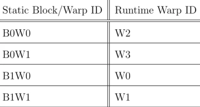
The load/store reordering across warps happens in the Reordering Unit, which reorders the memory accesses from different channels (i.e. warps). For instance, in the aforementioned PTX code example, there are 2 kernel blocks and 4 warps totally, including B0W0, B0W1, B1W0, and B1W1. Assuming the mapping between these warps and the runtime warp IDs is based on the mapping shown in Table 1, Fig. 13 gives 2 out of 24 possible orders of memory requests from the load/store unit.
The analysis results of the GPU L1 data cache analyzer are sent to the reorder-ing unit as the reorder configuration before a kernel is launched, which is used at runtime to decide how to reorder the memory accesses from different channels. The
Fig. 13. An Example of Memory Warp Instruction Reordering.[14]
Reordering Unit always searches in the reorder configuration for the warp (channel) with the smallest warp index (in a kernel block rather than runtime warp ID) and the smallest kernel block ID that still has the global load/store instruction with the lowest instruction address to execute. After the Reordering Unit gets a memory re-quest from that channel and sends it to the L1 data cache, it updates the reorder configuration so that it can move on and wait for a different channel or a different
Table 1. An Example of Mapping Between Static Block/Warp IDs and Runtime Warp IDs.
Static Block/Warp ID Runtime Warp ID
B0W0 W2
B0W1 W3
B1W0 W0
instruction at the same channel.
Fig. 14. An Example of Reorder Configurations.
An example is given in Fig. 14 to illustrate the load/store reordering process. The initial reorder configuration is depicted in Fig. 14 (a), based on which theReordering Unit knows it should wait at the channel 2 (i.e. CH2) for B0W0, because B0W0 is mapped toWarp 2 according to Table 1. Even if the requests from other warps have entered their channels, the Reordering Unit still waits at CH2 until it receives the memory request from the expected warp instruction and dispatches it to the L1 data cache. After this the reorder configuration is updated to be the one shown in Fig. 14 (b), based on which the Reordering Unit knows it should wait at CH3 for B0W1 now. The reordering process is continued and eventually the reorder configuration becomes what is shown in Fig. 14 (c) after the reordering unit has dispatched all the memory requests to the L1 data cache in the predictable order.
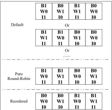
Fig. 15 shows the different sequences of the memory accesses to the L1 data cache in the above example in three schemes, including the default (i.e. dynamic warp scheduling), the pure round-robin warp scheduling, and the proposed reordering framework. In the default scheme, the access sequence to the L1 data cache can be arbitrary. When the pure round-robin warp scheduling policy is used, the warp scheduling order follows the runtime warp ID. Therefore, in this example the warps in kernel block B1 are scheduled before those in B0 according to the mapping between
Fig. 15. L1 Data Cache Access Orders of Different Schemes.
the warps in each kernel block and the runtime warp IDs as shown in Table 1. In the reordering framework, the sequence of the accesses is controlled by the reordering configuration as explained above. Therefore, both the reordering framework and the pure round-robin scheduling policy can improve the predictability in the sequence of GPU L1 data cache accesses, compared to the default system.
Fig. 16 uses the same example to demonstrate the performance differences be-tween different schemes. The meanings of the time points A to F are as shown in the figure. Due to the latency introduced by the reordering extension, the time point for a warp to be ready in the reordering framework may be later than those in the other two schemes, as shown in Fig. 16. Assuming there are 4 warps and the warp scheduler starts with W0, with the pure round-robin policy, the next warp is
W1, which will not be ready for a long period of time as shown in the figure. By comparison, the dynamic warp scheduler, which is used in both the default system
W2 W3 W0 W1 W2 W3 W0 W1 Reordering Framework Pure Round-Robin Time Delay of Pure Round-Robin Delay of Default Dynamic Warp Scheduling
W2 W3 W0 W1 Default System C D E A B F Delay Dynamic Warp Scheduling With Proposed Reordering Framework
C D E A B F W3 Ready in Default and Pure Round-Robin W2 Ready in Default and Pure Round-Robin W1 Ready in Default and Pure Round-Robin
W3 Ready in Reordering Framework W2 Ready in Reordering Framework W1 Ready in Reordering Framework
Fig. 16. Delay of Issuing Warp Instructions of Different Schemes.[14]
and the reordering framework, can choose to schedule other ready warps, i.e. W3
and then W2 in this example, before W1. As a result, the dynamic scheduler can lead to better performance, i.e. shorter delay as shown in the figure. However, due to the latency introduced by the load/store reordering, the delay of the reordering framework in this example is still larger than that of the default system, which also explains the performance overhead of the reordering framework as compared to the default scheme.
4.4.6 GPU L1 Data Cache Miss Rate Estimation
The abstract interpretation method [44] has been successfully used in the static timing analysis of cache memories for CPUs. Abstract Cache State (ACS) is used to analyze the content and behavior of the cache at a certain point in the program. As
shown in Fig. 17, every basic block has an initial ACSi and an exiting ACSe at the
beginning and the end respectively. The ACS is updated upon each memory reference. Therefore, the differences between theACSiandACSeof the same basic block depend
on the global memory instructions within this basic block. TheACSi is updated by
the memory references in the basic block using a specific cache replacing/updating policy, e.g. LRU.
The ACSi of the basic blocks with only one predecessor is the ACSe of its
predecessor, e.g. bothACSi(BB1) and ACSi(BB2) areACSe(BB0). If a basic block has more than one predecessor in the control flow graph, the ACSe of each of its
predecessor is joined together to form theACSi of this basic block, e.g. ACSi(BB3) = J oin(ACSe(BB1), ACSe(BB2)). The Join operation can be set intersection or set union depending on whether it is analyzed as an “always hit” or an “always miss”.
Fig. 17. An Example of Abstract Interpretation Based Static Timing Analysis. A basic assumption of the abstract interpretation is that the execution of the program only diverges and converges at the boundaries of basic blocks, not in between. It also assumes there is no interference between different program traces. In GPUs, however, these assumptions can only be guaranteed in the same warp, not across warps.
Recalling the example shown in Fig. 10, in abstract interpretation, theACSe(BB0) should be only decided by the content of BB0. However, due to the independent
ex-ecution of different warps, it is possible that when W0 and W2 are still in BB0, W1 is in BB2 already. In this case the ACSe(BB0) is affected by the content of BB2. In another scenario, if W0 is inBB1, W1 is in BB2 and W2 is in BB3, both ACSe(BB1) and ACSe(BB2) will be affected by the content in BB3. Therefore, the abstract interpretation cannot be applied to GPU caches directly, because the bound-aries between basic blocks are destroyed by the independent and dynamic execution of different warps. In the reordering framework, the boundaries are restored for global memory and data cache accesses despite the dynamic and independent execution of warps. For instance, after the reordering, no global memory accesses from BB1 or BB2 can access the L1 data cache until all the accesses from BB0 for all the active warps are done. Similarly, accesses from BB1 and BB2 need to be finished before accesses from BB3 can retrieve the L1 data cache.
In the proposed reordering framework, the worst-case GPU L1 data cache miss rate estimator uses the information of memory access addresses from the analyzer introduced in Section 4.4.4 and the reordering scheme introduced in Section 4.4.5 to generate the sequence of global memory access addresses for a CUDA kernel. This address sequence is used by the estimator to update the cache models with different configurations to estimate the worst cache miss rate of the GPU L1 data cache for this kernel. Since the sequence of L1 data cache accesses is predictable under the control of the warp-based load/store reordering framework, the miss rate estimator can statically analyze this sequence and generate accurate worst-case cache miss estimation.
4.4.6.1 Limitation of the GPU L1 Data Cache Timing Analyzer
Although the proposed framework can achieve accurate GPU L1 data cache miss rate with low performance overhead as our experiments indicate, not all types of
GPU kernels can be analyzed by our worst-case data cache miss analyzer currently. For example, GPU kernels with input-dependent branches and input-dependent data references cannot be analyzed. Also, the proposed framework requires knowing the loop upper bound statically, which is typical for WCET analysis.
4.5 Evaluation Results 4.5.1 Performance Results 0% 20% 40% 60% 80% 100% 120% 140% 160% 180% 200%
backprop gaussian lud nw srad Average
N o rm a liz ed Per fom ra nce R esul t w ith 16K L1 Data Cache
default 16K pure round-robin 16K reordering 16K
Fig. 18. Normalized Performance Results with 16KB L1 Data Cache.[14]
Figure 18 shows the normalized performance results (in terms of the total num-ber of execution cycles) of 3 different GPU configurations with a 16KB L1 data cache, which are normalized to the performance of the default configuration (i.e. dynamic warp scheduling without load/store reordering). Our experimental results show that the default warp scheduling has the best (average-case) performance as expected. However, the warp-based load/store reordering has much less performance overheads than the pure round-robin scheduling. This is because in the warp-based load/store reordering, instructions other than loads/stores are still scheduled by the
dynamic scheduling, which can dispatch a ready warp into execution faster than the pure round-robin scheduling. An average, the proposed reordering framework can achieve performance 24.4% better than that of the pure round-robin scheduling while achieving time predictability for the GPU data cache.
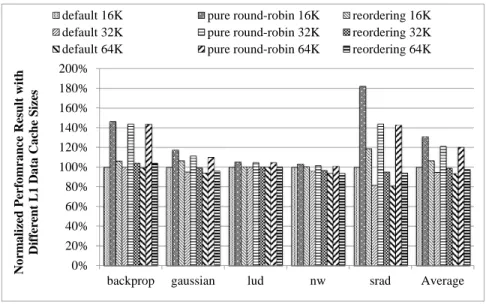
Figure 19 shows the normalized performance results of different cache sizes. The results are normalized to the performance results of the default configuration with the 16KB L1 data cache. As shown in the results, the reordering scheme has much better performance than the pure round-robin scheme and has only a small perfor-mance overhead compared to the default scheme without reordering for all these three different cache sizes.
0% 20% 40% 60% 80% 100% 120% 140% 160% 180% 200%
backprop gaussian lud nw srad Average
No rm a lized Per fo m r a nc e Res u lt w ith D iffer ent L1 Da ta Ca che Si zes
default 16K pure round-robin 16K reordering 16K default 32K pure round-robin 32K reordering 32K default 64K pure round-robin 64K reordering 64K
Fig. 19. Normalized Performance Results with Different L1 Data Cache Sizes.[14]
4.5.2 GPU L1 Data Cache Miss Rate Estimation Results
Figure 20 shows the simulated and estimated GPU L1 data cache miss rate results, which are normalized to the simulated miss rate, with a 16KB L1 data cache in each SM. The results show that the proposed estimator, together with the
channel-0% 20% 40% 60% 80% 100% 120%
backprop gaussian lud nw srad
N o rm a li zed Sim u la te d a nd Esi tm a te d L1 Da ta Ca ch e M is s Ra te s Simulated 16K Estimated 16K
Fig. 20. Miss Rate Estimation Results with 16KB L1 Data Cache.[14]
0% 20% 40% 60% 80% 100% 120%
backprop gaussian lud nw srad
Norm alized Si m u lated and Esitm a te d L 1 Da ta C a che M iss Ra tes
Simulated 16K Estimated 16K Simulated 32K
Estimated 32K Simulated 64K Estimated 64K
based reordering framework, can have very accurate estimation of the GPU L1 data cache miss rate. Figure 21 shows the simulated and estimated GPU L1 data cache miss rate results of 3 different cache sizes. The results show that the miss rate estimator can provide accurate miss rate estimations in different cache sizes.
CHAPTER 5
TIMING MODEL FOR STATIC WCET ANALYSIS OF GPU KERNELS
5.1 Introduction
To achieve high average-case performance and throughput, modern GPUs main-tains a massive number of active threads at the same time and uses a large number of on-chip cores to schedule and execute among these threads. The scheduling among the active threads is a dynamic behavior, which is very hard to analyze statically and harms the predictability. Moreover, the dynamic scheduling among different threads executing the same program code breaks the orders and relations of the instructions and basic blocks. Therefore, the traditional static analysis methods cannot be ap-plied to GPUs directly. Furthermore, the computing cores on a GPU chip are divided into groups, which are connected to the memory partitions through interconnection networks. The dynamic behavior of cores in competing for the memory resources is also hard to predict statically.
Therefore, before applying GPUs to real-time applications, the time predictabil-ity of the GPU architecture needs to be improved and analyzed. To address this problem, we proposed to employ the pure round-robin scheduling, which has pre-dictable behaviors, as the scheduling policy, based on which we propose a worst-case timing model for GPGPU programs. With the proposed timing model, a static an-alyzer, which can analyze the assembly codes of the GPGPU programs and give the WCET estimations, is also built. The evaluation results show that the proposed timing model and static analyzer can provide safe WCET estimations for GPGPU
applications.
5.2 Related Work
The studies on performance analysis of GPU architecture and GPGPU applica-tions [45][46][47][48] focus on building the performance and/or energy models. There are also studies focusing on building and analyzing the performance model of a spe-cific algorithm on GPU or heterogeneous platforms[49][50]. These studies mainly focus on the models of average-case performance and/or using the model to identify the performance bottleneck, while the performance model in this work focuses on the WCET estimation.
There are also studies on the GPU warp scheduling policies[51][52] to improve the efficiency in utilizing the computational resources and to access the memory in a more friendly way, so that the performance is improved. However, the proposed scheduling policy in this work focuses on improving the predictability of the GPU architecture. The memory access reordering method we proposed in [53] regulates the order of memory accesses to the GPU L1 data cache to improve the time predictability of the GPU L1 data cache, while the proposed scheduling policy and analyzer in this work focus on the timing model of the whole GPU system rather than just the L1 data cache.
There are some studies on GPU WCET analysis[54][55] using measurement-based methods, while the proposed WCET analysis method in this work is based on detailed analysis of the GPU architecture and can give safe WCET estimations for GPU kernels.
5.3 GPU WCET Analysis with Predictable Warp Scheduling
5.3.1 Pure Round-Robin Scheduler Timing Model
The method we propose is to use the pure round-robin warp scheduling policy, so that a timing model can be built for the execution of the warps in a GPU kernel. In this scheduling policy, the scheduler must issue one instruction one warp, before mov-ing to the next warp accordmov-ing to the order of warp IDs, as long as the current warp is not waiting at a synchronization barrier. Therefore, based on the dependencies between instructions, the PTX code of a GPU kernel can be divided into segments, each of which has one instruction and are called Code Segment. The dependencies between these code segments are decided by the contents of adjacent segments. The instruction in one code segment cannot be issued until the source operand with the longest latency is ready. Therefore, the latency between code segments can be es-timated by the dependencies among the instructions and the execution latencies of each instruction in a warp.
T00⇐0 Ti0 ⇐Ti00+LIi00(i >0) i0 = (i−1) (5.1) Tij ⇐M AX(Ti0k+LIi0k, Tij0 +LIij0 +LEij0) k = (i== 0) ? (j−1) : j i0 = (i== 0) ? (N −1) : (i−1) j0 =j−1 N :N umber of W arps (5.2)
![Fig. 4. Examples of different memory access patterns with different utilization rates.[13]](https://thumb-us.123doks.com/thumbv2/123dok_us/1080689.2643776/22.918.292.649.502.834/examples-different-memory-access-patterns-different-utilization-rates.webp)
![Fig. 6. Normalized total number of execution cycles with the L1 data cache without bypassing and with bypassing, and without the L1 data cache, which are nor-malized to that with the L1 data cache without cache bypassing.[13]](https://thumb-us.123doks.com/thumbv2/123dok_us/1080689.2643776/27.918.260.683.152.461/normalized-number-execution-cycles-bypassing-bypassing-malized-bypassing.webp)
![Fig. 8. Normalized L1 data cache miss rates with and without cache bypassing, which are normalized to that without cache bypassing.[13]](https://thumb-us.123doks.com/thumbv2/123dok_us/1080689.2643776/28.918.260.683.134.443/normalized-cache-rates-cache-bypassing-normalized-cache-bypassing.webp)
![Fig. 12. Warp-Based Load/Store Reordering Architectural Extension.[14]](https://thumb-us.123doks.com/thumbv2/123dok_us/1080689.2643776/40.918.257.682.135.433/fig-warp-based-load-store-reordering-architectural-extension.webp)
![Fig. 16. Delay of Issuing Warp Instructions of Different Schemes.[14]](https://thumb-us.123doks.com/thumbv2/123dok_us/1080689.2643776/44.918.218.720.130.527/fig-delay-issuing-warp-instructions-different-schemes.webp)
![Fig. 18. Normalized Performance Results with 16KB L1 Data Cache.[14]](https://thumb-us.123doks.com/thumbv2/123dok_us/1080689.2643776/47.918.226.713.390.686/fig-normalized-performance-results-kb-l-data-cache.webp)
![Fig. 21. Miss Rate Estimation Results with Different L1 Data Cache Sizes.[14]](https://thumb-us.123doks.com/thumbv2/123dok_us/1080689.2643776/49.918.227.714.615.965/miss-rate-estimation-results-different-data-cache-sizes.webp)
