DIGITAL CONTROL OF MULTI LEVEL
CASCADE INVERTER WITH
VARIABLE DC VOLTAGE SOURCES
S.NARASIMHA1
Research Scholar, Department of EEE, JNTUH, College of Engineering Hyderabad,
India, 500085, [email protected]
Dr.M.SUSHAMA2
Professor,
Department of EEE, JNTUH, College of Engineering Hyderabad,
India, 500085 [email protected] Abstract :
Cascade inverters have been widely an applied for the covering of high voltage and high power systems. The input power sources for an inverters needs separate DC voltage sources, if the fluctuations occur at the input voltage, The traditional method are difficult to implement conducting angels of switches to minimize the harmonic distortion of output voltage on a single chip, A switching control algorithm is proposed and validated for multilevel inverter with fluctuating DC voltage sources. In this paper simple control algorithm will proposed for multilevel inverter with variable DC voltage sources, we considered as a DC voltage ripples 10%, 15% and 20% for 27-level & 31-level inverter and the total harmonic distortion has Analyzed, the Simulations results are presented to the superiority of the proposed system.
Keywords: Cascade multilevel inverters; cogeneration systems; Switching control algorithm; Total
harmonic distortion.
1. INTRODUCTION
The demand of high power and low harmonic distortion ac power supplies has been increasing continuously. Among various converters , multilevel converters attracts lots of attention ,particularly. The series connection of multilevel converter modules reduces the voltage stress of each switch in a single phase full-bridge module (H-bridge), making the multi level converter s suitable for high power applications.[1-4].
However, the elementary concept of a multilevel converter to achieve higher power is to use a series of power semiconductor switches with several lower voltage dc sources to perform the power conversion by synthesizing a staircase voltage waveform. Capacitors, batteries, and renewable energy voltage sources can be used as the multiple dc voltage sources [2]. The commutation of the power switches aggregate these multiple dc sources in order to achieve high voltage at the output; however, the rated voltage of the power semiconductor switches depends only upon the rating of the dc voltage sources to which they are connected.
One of the limitations in these studies when the switching devices are operated at high voltage, switching frequency is restricted. With the advancement of power electronics and emergence of new multilevel converter topologies, it is possible to work at voltage levels beyond the classic semiconductor limits. The multilevel converters achieve high-voltage switching by means of a series of voltage steps, each of which lies within the ratings of the individual power devices. The multilevel inverter has gained much attention in recent years due to its advantages in high power with low harmonics applications. Multilevel inverters overcome this problem because their individual devices have a much lower voltage per switching and they operate at high efficiencies because they can switch at a much lower frequency than PWM-controlled inverters.[5-6]
gate drive and protection circuits. This may cause the overall system to be more expensive and complex [1][7-10].
Asymmetrical multilevel converters are an alternative to minimizing the harmonic distortion of the output voltages without increasing the number of switching devices. This paper suggests a new topology for multilevel inverters with a high number of steps associated with a low number of gate driver and protection circuits for switches. Reduction of rating of the switches is another advantage. The harmonic content is also reduced. A desired high output voltage is synthesized from several levels of dc voltages that can be batteries, capacitors, fuel cells etc.
An advantage of this approach is that isolated sources are not required for each phase. It should be noted that cascaded inverter systems can be considered from a number of different viewpoints. Considering the cascaded inverter to be one unit, it can be seen that a higher number of voltage levels are available for a given number of semiconductor devices. Considering the system as separate inverters, the cascaded design can be regarded as a combination of a bulk power (higher-voltage) inverter and a conditioning (lower-power) inverter. An alternate viewpoint is to consider the conditioning inverter as an active filter and the bulk inverter as the drive inverter. In any case, the cascaded multilevel inverter has several advantages for propulsion systems. One advantage is that cascaded inverters provide a compounding of voltage levels leading to extremely low harmonics. Another advantage is that the bulk inverter may be commercial-off-the-shelf; requiring that only the lower-power condition inverter to be custom made. [11-21].
2. Structure Of Multilevel inverters (27)-Level CMLI
The ratio of dc voltage sources affects the output voltage levels of a cascade multilevel inverter [1]. A multilevel cascade inverter consists of three converter modules in series is shown in fig. (1)
Fig.1. Single phase cascade 27-Level inverter
If the ratio of input dc voltages is VDC
: V
DC: V
DC1: 1: 1, the cascade inverter output voltage is
7-level, When the ratio of input dc voltages (:
:
) is 1:2:4 or 1:2:6, the cascade inverter output voltages is 15- or 19- level. Using separate dc voltage sources with ratio of VDC: V
DC: V
DC1: 3: 9, the
inverter output voltage is 27-level[1].Three dc voltage sources with a ratio of
:
:
1: 3: 9 are used in the proposed
system to obtain a 27-level inverter. A s shown in fig .2.7, three H-bridge inverter units are connected in series to form a multilevel output. Separate dc voltage sources are fed to inputs of the H-bridge inverter units. Control of the switching of the inverter units produces three output voltages , . String of the output voltages of H-bridge inverter units can obtain a nearly sinusoidal output waveform.[1]The ratio of separate dc voltage sources is as follows
VDC
: V
DC: V
DC1V : 3V : 9V
………(1) The output voltage of each H-bridge inverter unit can be obtained as follows:1V S
_, S
_ON
0V S
_, S
_ON
1V S
_, S
_ON
=
3V S
_, S
_ON
0V S
_, S
_ON
3V S
_, S
_ON
………(.3)
=
9V S
_, S
_ON
0V S
_, S
_ON
9V S
_, S
_ON
………(4)
The output Voltage ( ) of the cascade inverter is
v
v
v
v
…………..(5)
By using three H-Bridge inverter modules fed with separate dc voltage sources with the ratio of 1:3:9 and by controlling the switching of the inverter modules, an output of 27 voltage levels [1]can be generated. Table.2.3 shows the control of inverter modules in the cascade inverter to ranges from -13 to +13 (-13, -12, -11, ……, -2, -1, 0, 1, 2……., 11, 12, 13).
Table.1. Control of inverter modules for the 27 voltage levels
13 1+3+9 4 1+3+0 -9 0+0+9 12 0+3+9 3 0+3+0 -8 1+0-9 11 -1+3+9 2 -1+3+0 -7 -1+3-9
10 1+0+9 1 1+0+0 -6 0+3-9 9 0+0+9 0 0+0+0 -5 1+3-9
8 -1+0+9 -13 -1-3-9 -4 -1-3+0
7 1-3+9 -12 0-3-9 -3 0+3+0
6 0-3+9 -11 1-3-9 -2 1-3+0
5 -1-3+9 -10 -1+0-9 -1 -1+0+0
3. Structure Of Multilevel inverters(31)-Level CMLI
The ratio of dc voltage sources affects the output voltage levels of a cascade multilevel inverter. A multilevel cascade inverter consists of four converter modules in series is shown in fig. (2).
Fig.2. Single phase cascade 31-level inverter
If the ratio of input dc voltages is
:
:
:
1: 1: 1: 1, the cascade inverter output
voltage is 7-level , Using separate dc voltage sources with ratio of:
:
:
1: 2: 4: 8, the
inverter output voltage is 31-level[14].series to form a multilevel output. Separate dc voltage sources are fed to inputs of the H-bridge inverter units. Control of the switching of the inverter units produces four output voltages, String of the output voltages of H-bridge inverter units can obtain a nearly sinusoidal output waveform.
By using three H-Bridge inverter modules fed with separate dc voltage sources with the ratio of 1:2:4:8 and by controlling the switching of the inverter modules, an output of 31 voltage levels can be generated. Table.2. shows the control of inverter modules in the cascade inverter to ranges[14] from -15 to +15 (-15, -14, -13, ……, -2, -1, 0, 1, 2……., 13, 14, 15).
Table.2. Control of inverter modules for the 31 voltage levels
Voltage(Per Unit) Switching Patterns Voltage(Per Unit) Switching Patterns
15 1+2+4+8 -15 -1-2-4-8 14 2+4+8 -14 -2-4-8 13 1+4+8 -13 -1-4-8 12 4+8 -12 -4-8 11 1+2+8 -11 -1-2-8 10 2+8 -10 -2-8 9 1+8 -9 -1-8 8 8 -8 -8 7 1+2+4 -7 -1-2-4 6 2+4 -6 -2-4 5 1+4 -5 -1-5 4 4 -4 -4 3 1+2 -3 -1-2 2 2 -2 -2 1 1 -1 -1
4.CALCULATION OF SWITCHING ANGLE CASCADE INVERTER
To minimize the harmonic components of the output voltage of a cascade inverter, the switch angle for each H-bridge inverter needs to be calculated. A complex method usually used to obtain the switch angle of inverter module for traditional cascade inverter. A traditional five H-bridge cascade inverter can produce an 11- level output voltage which can be almost sinusoidal. Each switching angle of the inverter is calculated by Fourier series to eliminate the un desirable Harmonics[1][5-6].
cos θ
+cos θcos θ
cos θ
cos θ
=5*Micos 3θ
cos 3θ
cos 3θ
cos 3θ
cos 3θ
=0 cos 5θcos 5θ
cos 5θ
cos 5θ
cos 5θ
=0cos 7θ
cos 7θ
cos 7θ
cos 7θ
cos 7θ
=0cos 9θ
cos 9θ
cos 9θ
cos 9θ
cos 9θ =0
………….. (6)The modulation index is defined as Mi= , is the amplitude pf the reference voltage.
is the
maximum available output amplitude of the cascade inverter. For the five H-bridge cascade inverter,
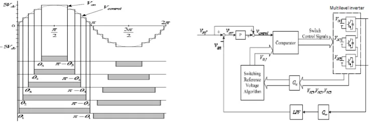
Fig.3. Structure and switching timing of conventional cascade inverter Fig.4. control block of proposed method
The method of obtain conducting angles of traditional cascade inverter has the merit of eliminating the required harmonic components, but it has some problems [1].
1. It is difficult to solve simultaneous nonlinear equations such as eq (6) .with traditional cascade multilevel inverters, 5 equations need to be solved for the 11-level inverter, If a 27- level cascade inverter is preferred, it is necessary to solve 13 equations.
2. The switching angles are calculated offline and stored in a look-up table the resolution of output voltage depends on the number of data in the look-up table. For contains ten modulations indexes (Mi=0.1, 0.2….1.0), the resolution of output voltage is 10% .To obtain the output voltage of resolution 1.0%. the look-up table o switching angles needs to contain a hundred modulation indexes (Mi=0.01, 0.02,….0.99, 1.0),
3. The switching angles of the traditional cascade inverter are calculated based on the assumptions that all dc input voltages sources are ideal. The variations of dc input voltage sources are ideal. The variations of dc input voltages will result in the increase o f output voltage harmonics.
4. It is difficult to accurately control the switching angles of inverter switches, thus results in the reduction of response speed and the increase of harmonic components. The control of switching timings of the H-bridge inverter is based on comparison of the time counter with the data in the look-up table which is built for various modulation indexes. Most of controllers are based on the use of a digital signal processor (DSP), therefore, a complex method is required to compensate for the errors from the iterative calculations and approximations of discrete data.
It proposes a simple method to calculate the switching angles for a cascade multilevel inverter. The proposed method transforms the computed switching angles into switching reference voltages to improve the above problems; an easy and accurate control can be achieved.
5. Multilevel Inverter Control Unit
The proposed digital control of multi level cascade inverter, as shown in Fig.4, consists of a switching reference voltage algorithm and a comparator. The function of switching reference voltage algorithm is to find out the switching angle for the inverter and the switching angles are transformed into the switching reference voltages .All the input voltages of H-bridge are feedback as input parameters to obtain the switching reference voltages. If variations of input DC voltage occur, the algorithm will take into account the variations and adjust the switching reference voltages for the inverter switches to reduce the output voltage harmonics[5-6][12][15]. The comparator is mainly designed to obtain the switching control signals to drive semiconductor power devices the voltage control signals (v ) and the switching reference voltages (v .) are compared to get the switching control signals, those dynamic control voltage can be easily achieved [1].
5.1. Switching reference voltage algorithm
Step-1: With the dc voltage inputs (V : V : V =1V : 3V : 9V ), the maximum output voltage of the cascade inverter is as follows.[1][22].
V
V
V
V
……… (7)Fig5. inverter.
Step-3: T
nominal
θ
: the aV
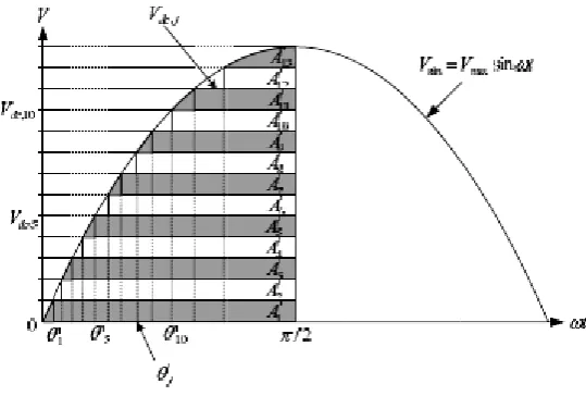
. : th during thThe areas cascade i
Step-4: T
A
,A , …
A
′A
′A
′A
eq(10) caA
A
The outpshows the no There are 13 v
The reference angles. θ
angle when the
he amplitude o he positive hal s of A ,
A , …
inverter [1].The area under
… . and A
.V
′ .sinV
′ .sinV
′ .sinV
.sinan be generali
V
.sinV
.sinput voltage (
Fig.5. Sine w
ominal switchi voltage levels
voltage equal
sin
VVe reference vo
of output volta lf cycle. In the
… . and A
ar the sine wav . The area of
n wtd wt
+n wtd wt
+n wtd wt
+n wtd wt
+zed and expre
n wtd wt
+wtd wt
+, ) with dc i
waveform and ste ing angles (θ s during positi
s the output v
.
, j=(1,2…
oltage is equal
age of cascade e case of a mu
are surrounde
ve form during
A
(j=1, 2….+ ′
V
,. d
+ ′
V
,. d
+ ′
V
,. d
+
V
,.
essed as follow
+
V
,. d
V
,. d
inputs voltage
ep-pulse areas in
) and the step ive half cycle, voltage (sin θ
….m) …………
l to the j ou
e inverter . m: ulti level outpu
ed by the sine
g the period of .m) can be ob
d wt
d wt
- A′d wt
- A′ -Ad wt
- A-w.
d wt
wt
- ∑A
e is shown in t
a multi level casc
p-pulse areas i ,
θ
=V .) at wt………….. (9)
utput level of t
the number o ut voltage, m i
wave form an
f (0~ ) is the tained as follo
A
′A
-……….AA
, j=2 … mtable 3.
cade inverter
in the propose
t = θ , the an
)
the cascade inv
of voltage leve is 13.The m is
nd the output v
e some of the ows.
A
……. (m ……… (11)
ed multi level
ngles are de
verter.
els of cascade s the integral n
Table.3. Output voltages of 27-level cascade inverter with input dc sources.
j j
13
V
DCV
DCV
DC 60
V
DCV
DC12
0
V
DCV
DC 5V
DCV
DCV
DC11
V
DCV
DCV
DC 4V
DCV
DC0
10
V
DC0
V
DC 30
V
DC0
9
0
0
V
DC 2V
DCV
DC0
8
V
DC0
V
DC 1V
DC0
0
7
V
DCV
DCV
DC 00
0
0
Fig.6&7. Real switching angles and the step pulse waves of output voltage
Fig.6. shows the output step-pulse weaves of a 27-level cascade inverter during the period of (0~ ) of sine waveform.
Step-5: The real switching angles θ (j=1,2…..13) are the switching controller for the inverter modules of cascade inverter. LetA
A
,The real switching angles θ can be obtained asθ
A VV . V , , j=1…m ……… (12) The V . is shown in table3.
The switching angle (θ) are calculated and used to control the switches of the cascade inverter.
For the conventional method, the switching angle
θ
(j=1,2…13) are calculated off-line for each modulation index . If the modulation indexes of (0.1, 0.2…..1.0) are considered, a table of ten switching patterns corresponding to these modulation indexes is stored in the controller. The accuracy of output voltage control for a cascade multilevel inverter depends on the amount of data stored in the table. With an on-line operation, lots o fluctuations required if the modulation index is varied.A simple method is proposed to obtain the switching angles for different modulation indexes.Fig6. Illustrates the concept of the proposed method, which transforms the real switching angles (θ) into the switching reference voltages
V
). As shown in Fig.6., the point (θ,V ). Is the intersection of the vertical line of wt=θ, and the sine wave form, V is the switching reference voltage for switching angle of θ.Step6: The switching reference voltages , ) can be obtained as follows.
V
,=V .sinθ
) j=1, 2…..m ………. (13)The output voltage
v
negative taken as the feed back to voltage referencev .5.2. Comparator for 27-level
V
P V
V
V
……….(14)Eq (14), V is the output reference voltage for the cascade inverter, and P is the proportional control.
The output voltage level counter (Nv) can be obtained by comparing voltage signals with the switching reference voltage V , , as shown in fig.7. The level counter Nv=j, if V =V ,. Two voltage control signals V =V sin (wt) and V =0.27 V sin(wt).
For the voltage control signal of sin (wt), the number of output level voltage level is 13 and Nv will be an integral number from +13 to -13. If the amplitude of voltage control signal is changed to 0.27 V , The number of output voltage is 4,and Nv is an integer from +4 to -4.
The output voltage level counter (Nv) is Transformed into switch control signals for the three inverter units, as shown in table 4.The switch control signals (P,N,Z) of inverter units have three potentials (positive, negative and zero) .
Table.4. Switch control signals of three inverter unit status.
Nv Nv
13 P P P -13 N N N
12 Z P P -12 Z N N
11 N P P -11 P N N
10 P Z P -10 N Z N
9 Z Z P -9 Z Z N
8 N Z P -8 P Z N
7 P N P -7 N P N
6 N N P -6 Z P N
5 N N P -5 P P N
4 P P Z -4 N N Z 3 N P Z -3 Z N Z
2 N P Z -2 P N Z
1 P N Z -1 N Z Z
If the output voltage level counter (Nv) is 8, the output status of inverter units are negative zero and positive potential (N,Z,P) respectively. Proper control of the switching devices in the inverter units produces three output voltages of v
Vdc , V
0 and
V
9vdc, the string of the output voltage of H-bridge
inverter units will be V =+8vdc.i) Calculation of 10% ripple voltage in 27-level inverters
V
D15 1
0.1 sin ωt
V , VD13.5V.
V
D45 1
0.1 sin ωt
1 3π
⁄
V, VD40.5V.
V
D135 1
0.1 sin ωt
2 3π
⁄
V
D121.5
ii) Calculation of 15% ripple voltage in 27-level invertersV
D15 1
0.1 sin ωt
V, VD12.5V.
V
D45 1
0.1 sin ωt
1 3π
⁄
V, VD38.5V.
V
D135 1
0.1 sin ωt
12 3π
⁄
V
D114.
iii) Calculation of 20% ripple voltage in 27-level invertersV
D15 1
0.1 sin ωt
V, VD12.3V.
V
D45 1
0.1 sin ωt
1 3π
⁄
V, VD36.2V.
V
D135 1
0.1 sin ωt
2 3π
⁄
V
D5.3. Comparator for 31-level
The inputs of comparator are voltage control signal ).and switching reference voltage ( , ).the voltage control signal ) can be obtained as follow [14].
V
P V
V
V
………. (15)In equation (15), is the output reference voltage for the cascade inverter, and P is the proportional control.
The output voltage level counter (Nv) can be obtained by comparing voltage signals with the switching reference voltage , ,as shown in fig.7. The level counter Nv=j, if V =V , .Two voltage control signals V =V sin(wt) and V =0.27 V sin(wt) as shown in fig.7.
For the voltage control signal of sin (wt), the number of output level voltage level is 15 and Nv will be an integral number from +15 to -15. If the amplitude of voltage control signal is changed to 0.27 V , The number of output voltage is 4,and Nv is an integer from +4 to -4.
The output voltage level counter (Nv) is Transformed into switch control signals for the three inverter units, as shown in table.5..The switch control signals (P,N,Z) of inverter units have three potentials (positive, negative and zero)[14] .
Table.5. Switch control signals of four inverter unit status
Nv Nv
15 P P P P -15 N N N N
14 Z P P P -14 Z N N N
13 P Z P P -13 N Z N N
12 Z Z P P -12 Z Z N N
11 P P Z P -11 N N Z N
10 Z P Z P -10 Z N Z N
9 P Z Z P -9 N Z Z N 8 Z Z Z P -8 Z Z Z N 7 P P P Z -7 N N N Z 6 Z P P Z -6 Z N N Z 5 P Z P Z -5 N Z N Z 4 Z Z P Z -4 Z Z N Z 3 P P Z Z -3 N N Z Z 2 Z P Z Z -2 Z N Z Z 1 P Z Z Z -1 N Z Z Z 0 Z Z Z Z
If the output voltage level counter (Nv) is 8, the output status of inverter units are zero, zero, zero and positive potential (Z, Z ,Z, P) respectively[14]. Proper control of the switching devices in the inverter units produces three output voltages of v
0 , V
0 , V
0 and
V
8vdc, the string of the
output voltage of H-bridge inverter units will be =+8vdc.i. Calculation of 10% ripple voltage in 31-level inverter VD
21.5 1
0.1 sin ωt
V, VD19.4V.
V
D43 1
0.1 sin ωt
1 3π
⁄
V, VD38.7V.
V
D86 1
0.1 sin ωt
2 3π
⁄
V
D77.4V.
V
D172 1
0.1 sin ωt
1 π
⁄
V,V
D154.8V.
ii. Calculation of 15% ripple voltage in 31-level inverterV
D86 1
0.1 sin ωt
2 3π
⁄
V
D73.1V.
V
D172 1
0.1 sin ωt
1 π
⁄ V
D146.2V
iii. Calculation of 20% ripple voltage in 31-level inverterVD
21.5 1
0.1 sin ωt
V, VD17.2V.
V
D43 1
0.1 sin ωt
1 3π
⁄
V,VD
34.4V.
V
D86 1
0.1 sin ωt
2 3π
⁄
VV
D68.8V.
V
D172 1
0.1 sin ωt
1 π
⁄ V
D137.6V
6. SIMULATION RESULTS6.1. 27-LEVEL CASCADE INVERTER
The simulation results are evaluated for a 27 level cascade inverters as the following.
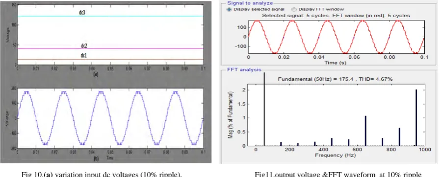
Fig.8. (a) shows the simulated results for the inverter powered from three ideal dc voltage sources with magnitude ratio of 1:3:9. The input dc voltages are =15v, =45v, =135v. The output voltage of cascade inverter (Vrms=200v) shown in fig.8 (b), The synthesized output voltage has 27- levels, which approximates an ideal sinusoidal wave form.
Fig.8. (a) Ideal dc input voltages (Vdc1:Vdc2:Vdc3 = 1:3:9), Fig 9.output voltage &FFT waveform (b) Output voltage wave form (Van).
The cascade inverters usually require several separate dc voltage sources, if the dc voltage is not ideal, the variation of input voltage sources will affect the harmonic distortion of output voltage. The proposed control can improve the harmonic distortion caused by the variation of input voltage sources.
Fig10.(a) shows the simulated results for the cascade inverter under the conditions of varied input voltages, which are =13.5v, =40.5v, =121.5v.
Fig 10.(a) variation input dc voltages (10% ripple), Fig11.output voltage &FFT waveform at 10% ripple (b) output voltage wave form (Van) with 10% ripple in Input DC voltage .
Fig 12.(a) shows the simulated results for the cascade inverter under the conditions of varied input voltages are =12.7v, =38.2v, =114v.
The ac ripples of three voltage sources are 15% and phase shifted with respect to each other for worst condition of the input dc voltages. Fig 12. (b) Shows the output voltage of cascade inverter (Vrms=166V) which approximating an ideal sinusoidal waveform.
Fig. 12(a) variation input dc voltages (15% ripple),(b) output voltage wave form (Van)
Fig 13.(a) shows the simulated results for the cascade inverter under the conditions of varied input voltages are =12v, =36v, =108v.
The ac ripples of three voltage sources are 20% and phase shifted with respect to each other for worst condition of the input dc voltages. Fig 13.(b) shows the output voltage of cascade inverter (Vrms=156v) which approximating an ideal sinusoidal waveform.
Table6. Parameters of proposed cascade inverter
6.2. 31-LEVEL CASCADE INVERTER
The simulation results are obtained for a 31–level cascade inverter as following,
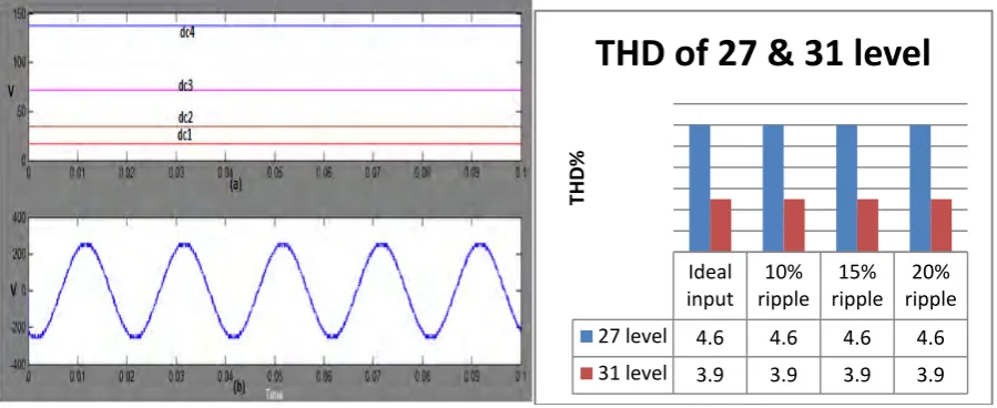
Fig.14.(a) shows the simulated results for the inverter powered from four ideal dc voltage the sources voltage with magnitude ratio of 1:2:4:8. The input dc voltages are = 21.5v, =43v, =86v and =172v, the output voltage of cascade inverter (Vrms=318V) shown in fig .14.(b) ,The synthesized output voltage has 31 levels, which approximate s an ideal sinusoidal wave form .
Fig.14. (a) Ideal dc input voltages (Vdc1:Vdc2:Vdc3:Vdc4=1:2:4:8), Fig 15. Output voltage waveform and FFT (b) output voltage wave form (Van)
Fig 16(a) shows the simulated results for the cascade inverter under the conditions of varied input voltages are =19.4v, =38.7v, =77.4v and =154.8v. The ac ripples of three voltage sources are 10% and phase shifted with respect to each other for worst condition of the input dc voltages, Fig 16(b) shows the output voltage of cascade inverter (Vrms=285) which approximating an ideal sinusoidal waveform.
Fig. 16 (a) variation input dc voltages (10% ripple), Fig 17. Output voltage & FFT waveform 10% ripple (b) output voltage wave form (Van).
Parameters Value Phase Single Frequency 50HZ
V
DC 15VV
DC 45VV
DC 135VFig18(a) shows the simulated results for the cascade inverter under the conditions of varied input voltages are = 18.27v, =36.5v, =73.1v and =146.2v.
The ac ripples of four voltage sources are 15% and phase shifted with respect to each other for worst condition of the input dc voltages, Fig18 (b) shows the output voltage of cascade inverter (Vrms=270V) which approximating an ideal sinusoidal wave form.
Fig. 18 (a) variation input dc voltages (15% ripples), (b) output voltage wave form (Van).
Fig 19 (a) shows the simulated results for the cascade inverter under the conditions of varied input voltages are = 17.2v, =34.4v, =68.8vand =137.6v. The ac ripples of three voltage sources are 20% and phase shifted with respect to each other for worst condition of the input dc voltages, Fig 19(b) shows the output voltage of cascade inverter (Vrms=256) which approximating an ideal sinusoidal wave form.
Fig. 19.(a) Variation input dc voltages (20% ripple), and Fig 20. THD Comparison of 27- level and 31-level (b) output voltage wave form (Van).
Results Comparison
The comparison between the total harmonic distortion of 27 and 31-level cascaded inverter 10%,15% and 20% ripple voltage an evaluated in fig.20. It can be observed that the THD is better in 31- level inverter shown in Fig 20.
7. CONCLUSION
The simulation results for 27-level and31-level cascaded inverters are evaluated in this paper. Their harmonic analysis is an examined in from Fig 8-13 to Fig 14-19. The THD of the cascaded multi-level inverters have been calculated at different modulation index. The simulation results validated that the proposed method satisfactory performance up to 20% ripples in dc voltage fluctuations.
FUTURE SCOPE
The control technique for multilevel power converters can be further simplified and generalized to different levels and other class of power converters and inverters. The levels of multilevel configuration can be increased and further improvements in terms of performance and power quality issues can be broadly studied and could be implemented with hardware circuits.
Ideal
input
10%
ripple
15%
ripple
20%
ripple
27 level 4.6 4.6 4.6 4.6
31 level 3.9 3.9 3.9 3.9
THD%
The same cascaded multilevel inverter configuration can be installed for other applications like SVC The quality of the power supplied to the consumers and electrical utilities should adhere to the stringent norms prescribed for the power quality. In this paper, we examined the ripple voltage up to 20% the harmonic distortion is constant. After 20% harmonic distortion wills increasing then we should goes to next level to reduce the harmonic distortion.
REFERENCES
[1] Chih. Chiang Hua, Chun. Wei We, Chih. Wei Chuang, “Fully Digital Control Of a 27 level Cascade Inverter With Variable DC Voltage Sources ” , IEEE Industrial Electronics and applications, pp. 2441-2448, May 2007.
[2] E. Najafi, Yatim, and A.H.M , “Design and Implementation of a New Multilevel Inverter Topology” IEEE Transactions on Industry Electronics, vol. 59, no.11, pp. 4148-4154, Nov 2012.
[3] N. A. Rahim , k. Chaniago and j. Selvaraj "single-phase seven-level grid-connected inverter for photovoltaic system", ieee trans.ind. Electron., vol. 58, no. 6, pp.2435 -2443, 2011.
[4] M. Malinowski , k. Gopakumar , j. Rodriguez and m. A. Pérez "a survey on cascaded multilevel inverters", ieee trans. Ind. Electron., vol. 57, no. 7, pp.2197 -2206, 2010.
[5] K. Jang-hwan , s.-k. Sul and p. N. Enjeti "a carrier-based pwm method with optimal switching sequence for a multilevel four-leg voltage-source inverter", ieee trans. Ind. Appl., vol. 44, no. 4, pp.1239 -1248 2008.
[6] D. W. Kang, H. C. Kim, T. J. Kim and D.S. Hyun “A simple method for acquiring the conducting angle in a multilevel cascaded inverter using step pulse waves”, IEE Proc-Electr. Power Appl., vol. 152, no. 1, pp. 103-111, January 2005.
[7] Y. S. Lai and F.S. Shyu, “ Topology for hybrid multilevel inverter”, IEE Proc-Electr. Power Appl., vol. 152, no. 1, pp. 103-111, January 2005.
[8] V.G. Agelidis, A. Balouktsis and M. S.A. Dahidah, "A five-level symmetrically defined selective harmonic elimination PWM strategy: analysis and experimental validation," IEEE Trans. on Power Electronics, vol. 23, no. 1, pp. 19-26. January 2008,
[9] M.S.A. Dahidah, G. Konstantinou and V.G. Agelidis, "SHE-PWM and optimized DC voltage Levels for cascaded multilevel inverters control," in IEEE ISIEA pp. 143-148, 2010.
[10] Suroso , T. Noguchi. “A Multilevel Voltage-Source Inverter using H-Bridge and Two-Level Power Modules with a Single Power Source”. IEEE International Conference on Power Electronics and Drive System (PEDS). pp. 262-266, 2011.
[11] J. I. Leon, S. Kouro, S. Vazquez, R. Portillo, L. G. Franquelo, J. M. Carrasco, and J. Rodriguez, “Multidimensional modulation technique for cascaded multilevel converters,” IEEE Trans. Ind. Electron., vol. 58,no. 2, pp. 412–420, Feb. 2011.
[12] J. H. Kim, S. K. Sul, and P. N. Enjeti, “A carrier-based “PWM method with optimal switching sequence for a multilevel four-leg voltage-source inverter,” IEEE Trans. Ind. Appl., vol. 44, no. 4, pp. 1239–1248, Jul./Aug. 2008.
[13] J.Lai and F.Z .Peng , “Multilevel converters-a new breed of power converters ” , IEEE Transactions on Industry applications, vol. 32, no.3, pp. 509-517, May/June 1996.
[14] C.K. Lee, S.Y.Ron Hui, and H.S. Chung, “A 31-level cascade inverter for power applications” IEEE Transactions on Industry Electronics, vol. 49, no.3, pp. 613-617, June 2002.
[15] B.P.McGrath, and D.G. Holmes ,”Multicarrier PWM strategies for multilevel inverters” IEEE Transactions on Industry Electronics, vol. 49, no.4, pp. 858-867, August 2002.
[16] J. Rodriguez , L. Moran, J. Pontt, and C. Silva, “A high-performance vector control of an 11-level inverter” IEEE Transaction on Industry Electronics, vol. 50, no.1, pp. 80-85, February 2003.
[17] B.P.McGrath, and D.G. Holmes , “Opportunities for harmonic cancellation with carrier-based PWM for a two-level and multilevel cascade inverters” IEEE Transactions on Industry Electronics, vol. 37, no.2, pp.574-582, March/April 2001.
[18] A.M. Almaktoof, A.K. Raji, and M.T.E. Kahn “Robust current control technique for variable DC-link Voltage Source Inverters for Renewable Energy Systems,” IEEE Industrial and commercial use of energy(ICUE)no. 2, pp. 1–8, August. 2014.
[19] T.S Radwan, M.A. Rahman, A.M Osheiba, A.E Lashine, “Digital current control techniques for voltage source inverters,” IEEE Trans. Electrical and computer Engineering, vol. 2, pp.1124–1127, Sep 1995.
[20] M. Pande, G. Joos, K. Jin, and P.D. Ziogas, “Output voltage integral control technique for compensating a non-ideal DC bus in voltage source inverters,” IEEE Trans. Power Electronics, vol. 12, pp.302–310, Mar 1997.
[21] Yaow-Ming Chen, Yuan-Ming Cheng “Modified PWM control for the DC-AC inverter with a non-constant voltage source,” IEEE Trans. Power Electronics and Drive system , vol. 2, pp.938–941, Jul 1999.