An Efficient D-Flip Flop using Current Mode
Signaling Scheme
Sheona Varghese Anu Raj
PG Scholar Assistant Professor
Department of Electronics & Communication Engineering Department of Electronics & Communication Engineering Saintgits College of Engineering Saintgits College of Engineering
Jyothish Chandran G
Assistant Professor
Department of Electronics & Communication Engineering Saintgits College of Engineering
Abstract
In this paper a power efficient D-flip flop was conducted by adopting a current mode signalling scheme (CMS), named current mode clocked D-flip flop. For providing full swing output proposed D-flip flop is constructed by transmission gate with Clock gating. This setup reduces the dynamic power dissipation and also reduces the circuit complexity. In this project, the effect of current mode scheme on power as well as performance of flip flop such as MS D-FF, DDFF, CPEFF and CMPFFE are analysed. The performance analysis was carried out by adopting 180nm CMOS technology. Experimental results reveal that current mode clocked D-flip flop outperforms the conventional flip flop in terms of power, delay and power delay product.
Keywords: Conditional Pulse Enhancement Scheme, Dual Dynamic Node, Current Mode Pulsed, Current Mode Clocked, Clock Gating, Transmission Gate
________________________________________________________________________________________________________
I. INTRODUCTION
In VLSI design, researchers are interested greatly in the design of the system with high speed, less area and that are power efficient. Nowadays portable devices are increases, the need is large battery life. This can be obtained by low power components. Technology scaling shows that delay of local interconnects reduces, but the global interconnect delay increases. Flip flops are one of the major modules in all digital storage element. Nowadays many schemes are adopted to increase the efficiency of the flip flops. The main power consumers in flip flops are clock network and interconnect. By using high-speed signalling schemes the dynamic power consumption of this clock network can be reduced.
Mainly there are two types of high-speed signalling schemes are available, named as voltage mode and current mode signalling. Voltage mode (VM) and current mode (CM) are the two regulating conditions that control the output of the supply. Most of the application uses a voltage source as supply, VM supply constant output voltage whereas the current drawn from 0 to full rated current of the supply. Generally, voltage sources are modelled as providing low output impedance. The Current mode works in a similar manner but its limits and regulates the output current to the desired level, so it provides constant current to each load. The current mode is modelled as very high output impedance [3]
Current mode logic was a pleasing high-speed signalling scheme, however, they consume more static power. In case of increasing interconnect delay and power consumption, current mode logic gives better results than VM because in CM it transmit current with minimal voltage swing to each load and at output gives full swing.
In this paper present an efficient flip flop using current mode signaling scheme with clock gating technique, where the clock distributed to the interconnect as Current. . The rest of the paper is organized as follows: Section II describes some of the existing flip flop design. Section III proposes an efficient D-flip flop and clock distribution network. Section IV compares new CM flip flop with some existing flip flop design and also compares its application, followed by conclusion in Section V.
II. ANALYSIS OF FLIP FLOP ARCHITECTURES
Conventional Master Slave Flip Flop
Master slave flip flop are implemented by placing two static latches back to back. First latch output follows the input when clock is LOW and second latch output follows the input when clock is HIGH and called as positive edge triggered flip flop. In order to reduce the delay either first or the last inverter can be removed. The flip flop usually generate single clock signal and locally generate its compliment. Making both the latches transparent increasing the flip flop hold time. Fig 1 shows the master slave flip flop.
Fig. 1: Master Slave Flip Flop
Conditional Pulse Enhancement Flip Flop
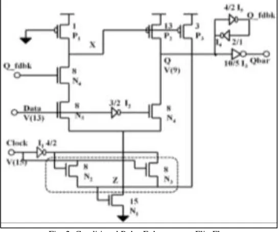
Fig 2 shows the conditional pulse enhancement flip- flop (CPEFF). This structure reduced the number of nMOS transistor stacked in the discharging path and enhance the pull -down strength when the input data is ‘1’.Transistor N2 and N3 combined to form a two input AND gate logic, which control the discharge of N1 transistor. Complementary inputs are given to the AND gate, and most of the time output kept to zero. During the falling edge of the clock, floating at node Z is harmless
Fig. 2: Conditional Pulse Enhancement Flip Flop
Dual Dynamic Node Flip Flop
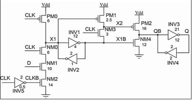
Fig 3 shows the Dual Dynamic Node Flip Flop (DDFF) flip -flop structure. In this architecture node, X1 is pseudo -dynamic and node X2is purely dynamic. The weak inverter acts as a keeper. Instead of conditional shutoff mechanism in Cross Charge Control Flip-Flop (XCFF) here unconditional shutoff mechanism is provided at the front end. This flip flop operated in two phases the first phase when the clock is “HIGH” called evaluation phase, the second is when the clock is “LOW” called precharge phase. During the evaluation phase, 1-1 overlap of CLK and CLKB occurs. If D is high prior to this overlap period, node X1 is discharged through transistor NM0 to NM2.This cause node X1B to go high and output QB to discharge through NM4 [14].The low level at the node X1 is retained by the inverter pair INV1 to INV2 for the rest of the evaluation phase where no latching occurs. Thus, node X2 is held HIGH throughout the evaluation period by the pMOS transistor PM1.As the CLK falls LOW, the circuit enters the precharge phase and node X1 is pulled high through PM0.During this time node X2 is not actively driven by any transistor, it stores the charge dynamically. The output at node QB and maintain their voltage levels through INV3-4.
Fig. 3: Dual Dynamic Node Flip Flop
Current Mode Pulsed Flip Flop with Enable
Fig 4 shows the current mode pulsed flip -flop with enabling architecture. This circuit uses an input current comparator stage, a register stage, and a static storage cell. The current comparator stage compares the input push -pull current with the reference current and amplifies the clock to a full swing voltage pulse that triggers the data to latch at the register stage [9]. This CMPFF is only sensitive to the unidirectional push-pull current which gives the positive edge trigger operation of the flip- flop. This structure provides an active low enable signal.
III. PROPOSED ARCHITECTURE
In past decades several modified flip flops have been proposed, all aiming at the reduction of power delay and area. The major power consuming module in flip -flop is clock distribution network. In this paper proposed a D-flip flop using current mode signalling scheme. Current mode signalling is one of the high -speed signaling scheme. Also provide a clock gating to proposed flip -flop, reduce the unwanted switching activities. Therefore the delay and overall power performance of the proposed flip- flop reduced.
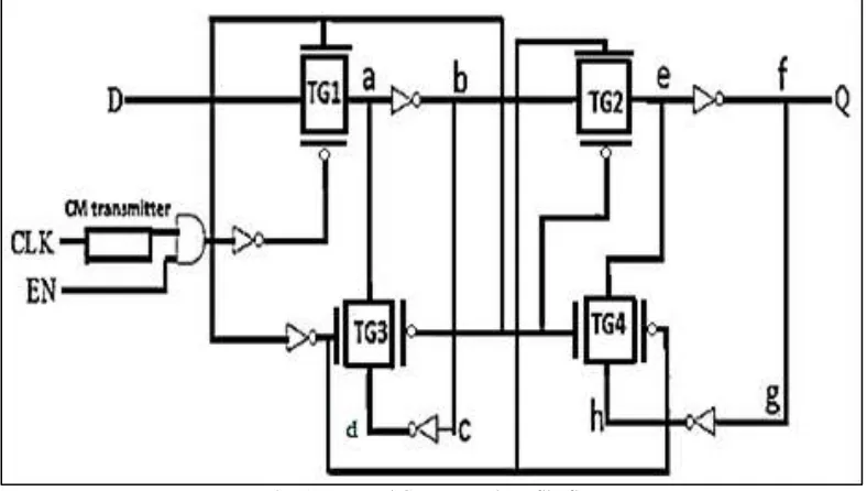
Fig. 5: Proposed Current mode D-flip flop
Fig 5 shows the proposed Current mode clocked flip- flop. The circuit is implemented by a transmission gate, buffers, and a AND gate. Clock supplied to the circuit as current rather than voltage. Clock gating is provided by an AND gate logic, so only when the enable input is 1 the clock signal comes in from to the circuit. This will reduce the unwanted switching activates in the circuit. Using transmission gate got full swing output, so dynamic power will be reduced. First latch stage is ON only when the clock is HIGH, during this period the second latch is inactive. When the clock is LOW the second latch is ON and holds its previous value. Only strong values are transmitted by two latch structures, hence gets a full swing at the output.
Current Mode Transmitter
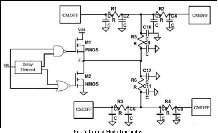
To integrate the current mode D flip- flop using transmission gate, we required a trusted transmitter that can provide a push- pull current to the clock network and distribute the required amount of current to each current mode D flip -flop. The transmitter used is similar to the transmitter used in reference [9].Clock distribution network consists of a transmitter, RC interconnect model and proposed current mode D flip -flop shown in Fig 6.
Input given to the transmitter is a conventional voltage mode clock and at the output provide a push -pull current, this push- pull current is distributed to the interconnect line so required amount of current is given to each CMDFF. Clock distribution network is modelled as symmetric H-tree [10] so that equal current is distributed to each CMDFF. In fig 6, positive edge clock and its delayed inverted clock are the input of NAND gate, produces a small negative pulse will turn on the transistor M1, hence PMOS transistor source the line to Vdd. Similarly, NOR gate uses the negative edge of the clock and its delayed inverted clock will produce a small pulse will turn on the transistor M2 while M1 is off, hence the NMOS transistor sinks the line to ground.
Fig. 6: Current Mode Transmitter
IV. EXPERIMENTAL RESULTS
In order to evaluate the proposed design, the performance of the proposed D-flip flop design is evaluated against the existing design. To create the schematic of the circuit Pyxis schematic of Mentor Graphics is used. The performance of the proposed design is compared with the existing design through pre-layout simulations using Eldo simulator and output waveforms are viewed using E-Z wave viewer. All the circuits have been simulated in TSMC 180nm CMOS technology with VDD of 1.8V.
Table 1 illustrates the delay and power delay product of various flip flop with the proposed flip flop design. The results shows that the proposed design have lowest power dissipation among the group and also the CLK to Q delay is much less compared to other flip flops.
Table – 1
Performance Comparison of Various Flip Flops with Proposed Current mode Clocked D-Flip Flop Flip Flop Total Power (µW) CLK – Q Delay (pS) PDP (pJ)
MS DFF 201.72 447.46 0.0926
CPEFF 231.385 247.70 0.0573
DDFF 281.21 742.25 0.0208
CMPFFE 1.265M 5.460n 6.9069m
Proposed CMDFF 6.959 447.29 0.0031
Flip flops had several number of application like it can be used in shift registers, counters, register files etc. Table 2 shows the comparison of Johnson counter using proposed D-flip-flop with traditional flip flop. Results shows that the power dissipation and CLK to Q delay of proposed counter with proposed flip flop have less power compared to that of counter using conventional flip flop. And the proposed flip flop design gives 25.62% decrease in total power delay product.
Table – 2
Comparison of Johnson counter using proposed flip flop and Johnson counter using traditional flip flop Circuit Power Dissipated (µW) CLK to Q Delay (pS) 4-Bit Johnson counter using conventional Flip flop 179.641 235
4-Bit Johnson counter using proposed D-Flip flop 152.407 206
V. CONCLUSION
REFERENCES
[1] Sylvester, Dennis, and Chenming Wu. "Analytical modeling and characterization of deep-submicrometer interconnect." Proceedings of the IEEE 89.5 (2001): 634-664.
[2] Guthaus, Matthew R., Gustavo Wilke, and Ricardo Reis. "Revisiting automated physical synthesis of high-performance clock networks." ACM Transactions on Design Automation of Electronic Systems (TODAES) 18.2 (2013): 31.
[3] Yamashina, Masakazu, and Hachiro Yamada. "An MOS current mode logic (MCML) circuit for low-power sub-GHz processors." IEICE Transactions on Electronics 75.10 (1992): 1181-1187.
[4] Seevinck, Evert, Petrus J. van Beers, and Hans Ontrop. "Current-mode techniques for high-speed VLSI circuits with application to current sense amplifier for CMOS SRAM's." IEEE Journal of Solid-State Circuits 26.4 (1991): 525-536.
[5] Kwon, Chang-Ki, Kwang-Myoung Rho, and Kwyro Lee. "High speed and low swing interface circuits using dynamic over-driving and adaptive sensing scheme." VLSI and CAD, 1999. ICVC'99. 6th International Conference on. IEEE, 1999.
[6] Dave, Marshnil, et al. "A variation tolerant current-mode signaling scheme for on-chip interconnects." IEEE Transactions on Very Large Scale Integration (VLSI) Systems 21.2 (2013): 342-353.
[7] Dave, Marshnil Vipin, Maryam Shojaei Baghini, and Dinesh Kumar Sharma. "A process variation tolerant, high-speed and low-power current mode signaling scheme for on-chip interconnects." Proceedings of the 19th ACM Great Lakes symposium on VLSI. ACM, 2009.
[8] Weste, Neil HE, and David Harris. "CMOS VLSI DESIGN A circuts and systems perspective Forth Edition." (2010): 120.
[9] Islam, Riadul, and Matthew R. Guthaus. "Low-Power Clock Distribution Using a Current-Pulsed Clocked Flip-Flop." IEEE Transactions on Circuits and Systems I: Regular Papers 62.4 (2015): 1156-1164.
[10] ISPD, ISPD 2009 Clock Network Synthesis Contest [Online]. Available: http://ispd.cc/contests/09/ispd09cts.html.
[11] Zhang, Liang, et al. "A 32-Gb/s on-chip bus with driver pre-emphasis signaling." IEEE Transactions on Very Large Scale Integration (VLSI) Systems 17.9 (2009): 1267-1274.
[12] Kozu, S., et al. "A 100 MHz, 0.4 W RISC processor with 200 MHz multiply adder, using pulse-register technique." Solid-state circuits conference, 1996. Digest of technical papers. 42nd ISSCC., 1996 IEEE International. IEEE, 1996.
[13] Hwang, Yin-Tsung, Jin-Fa Lin, and Ming-Hwa Sheu. "Low-power pulse-triggered flip-flop design with conditional pulse-enhancement scheme." IEEE transactions on very large scale integration (VLSI) systems 20.2 (2012): 361-366.