TEMPERATURE SWITCHING ANALYZER
Mrs. S. J. KULKARNI, PROF. S. N. PAWAR, Ms. M.S.TADPATRIKAR
ABSTRACT:Electrical characterization, such as measurement of the I-V characteristics of electronic devices with respect to change in temperature is
necessary for application of such devices. In our project, we report the development of a simple low-cost system for the measurement of I-V characteristics associated with changing surrounding temperature. The temperature switching analyzer developed basically consists of a PIC micro controller based Master/Slave configuration for monitor and control for electronic devices along with high-speed data acquisition system. The design aspects of the system, its interface.' to the high-speed data acquisition system and the personal computer, and the details of the application software developed are described.
KEY WORDS: I-V characteristics, PIC micro controller, Temperature switching analyzer
————————————————————
1. INTRODUCTION
The aim is to design and implement a simple low cost Electrical/Electronic temp switching analyzer. The hardware components of the system consists of micro controller based Master/Slave configuration for temp monitor and control and a high-speed data acquisition system for current and voltage ratings. The Master controller is designed for temperature monitoring and is visualized by LCD. LM35 is used as a temp sensing device. As the temperature monitored and when the upper and lower cut off temp is set the heating chamber power is made on until the max temp is reached. As the max temp is obtained the AC power is made off. Relays are used to control these actions. The Master PIC microcontroller controls three relays; one of them is used for controlling the heating chamber operation. Second and Third relay are used to operate the temp sensing electronic devices. The analog values given out by the temp sensing devices are converted to digital signals and passed to computer through serial communication protocol. The Slave PIC microcontroller does the operation of digital conversion of analog inputs coming in from two channels. A switching mechanism is utilized here so that the DAC comes into picture and the Slave generates sine, square, triangular waves. The application software is continuously waiting for the digital data coming from the hardware and is designed to develop the graphical presentations such as 1) Voltage v/s Time 2) Current v/s Time 3) Voltage v/s Current. The application s/w is developed in VB6.0. It is designed to generate the respective characteristic graph as well as it has got facility to store the data in database and resume when ever required.
2. FEATURES OF THE PROJECT
The protocol developed consists of various electronic monitoring and controlling protocols like-
a) It can work as computer operated digital thermometer for indication of room temperature as well as storage of the variations with respect to time.
b) A PIC16f 877A microcontroller based Master temperature controlling device which controls the heating chamber switching.
c) 16x2 LCD display to display the temperature.
d) A Sine, Triangular and square wave generation using DAC 0800.
e) The application software can also be used as signal storing device as the signal coming in digital binary form is stored and can be re produced as per requirement at times.
3. FUNCTIONAL BLOCK DIAGRAM
Fig.1 shows the block diagram of Electrical/ Electronic switching analyzer. The various blocks are explained as follows. The design of each sub-block is also explained. A. Signal conditioning block
Signal conditioning is widely used term in the world of data acquisition. The most common transducers produce an output in the form of voltage, current, charge, capacitance and resistance. However, we need to convert these signals to voltage in order to send input to A-to-D converter. This conversion is commonly called as signal conditioning. The Temperature sensors components used in the protocol are LM-35
B. Microcontroller-Based Wave Form Generation Source
The microcontroller-based Wave Form Generation source is designed to function as a programmable voltage Wave Form Generation source depending on the parameter given through hyper terminal. This unit has features to generate different types of waveforms such as triangular, ramp, step. etc. with single or multiple cycles. The instrument receives the commands from the computer through the serial port and outputs the required different types of waveforms such as triangular, ramp, step. etc
___________________ 1. Mrs. S. J. KULKARNI, 2. PROF. S. N. PAWAR 3. Ms. M.S.TADPATRIKAR
1. Sr. Lecturer, E & TC Dept., P.D.V.V.P. Polytechnic, Loni. 2. Asst. Prof., E & TC Dept. , JNEC, Aurangabad.
3. Sr. Lecturer, E & TC Dept., Modern College of Engg, Pune.
C. Microcontroller-Based Temperature controller and Monitoring System
It consists of a transformer, rectifier, filter, a digital-to-analog converter (DAC).A in build ADC module, A pair of PIC 16f877 microcontroller boards in master slave configuration for intelligent control, Relay board with relay drivers an RS-232 driver to interface to the computer, and the associated power supplies.
D. PIC micro controller
Microcontroller is the heart of this system. It handles all the operations of the system. In this dissertation PIC16F877 is used. It is a 8-bit PIC microcontroller (PIC16F877) having 16-kB EPROM, 256-B RAM, three 16-bit timer/counters, and four 8-bit bi-directional ports.
4. HARDWARE DESIGN
The Master PIC microcontroller controls three relays; one of them is used for controlling the heating chamber operation. Second and Third relay are used to operate the temp sensing electronic devices. The analog values given out by the temp sensing devices are converted to digital signals and passed to computer through serial communication protocol.
The Slave PIC microcontroller does the operation of digital conversion of analog inputs coming in from two channels. A switching mechanism is utilized here so that the DAC comes into picture and the Slave generates sine, square, triangular waves. Thus the project can be viewed as consisting of four modules, namely,
Master Temperature Monitoring Unit Master Temperature Controlling Unit
Slave ADC and Serial communicating protocol Slave Waveform Generator Unit
Following figure shows block diagram for Electrical /Electronic Temperature Switching Analyzer.
Figure 1: Block Diagram of Electrical /Electronic Temperature Switching Analyzer
230/ACHeater Electronic Component
230V AC MASTER
PIC 16F877A
LCD
Relay Driver
Relay
LM35 Signal
Conditioning
Power Supply
PIC 16F877A
Waveforms
Application Software
Max 232 or Transistor
Relay Power
Source
Relay Power
Source Power
Supply
Signal Conditioning for Electronic Component
DAC
Microcontroller Interface
To LCD Pin 4(RS)
C
R4
RESISTOR SIP 10
1 2 3 4 5 6 7 8 9 10 R9 RESISTOR D7 DIODE ZENER
To LCD Pin 12(D5)
C1 1000UF/25V D3 DIODE VCC D2 DIODE C R8
RESISTOR SIP 9
1 2 3 4 5 6 7 8 9 R12 RESISTOR C R7 RESISTOR SIP 9
1
23456789
R1 10K
VCC
To LCD Pin 13(D6)
VCC C7 CAP NP J9CON12 1 2 3 4 5 6 7 8 9 10 11 12 C4 CAP NP
To LCD Pin 6(E)
C3 CAP NP U2 LM7805C/TO 1 3 2 IN OUT GN D C6 CAP NP VCC U1 AT89S8252 9 18 19 20 30 24 31 40 1 2 3 4 5 6 7 8 21 22 23 25 26 27 28 29 10 11 12 13 14 15 16 17 39 38 37 36 35 34 33 32 RE1/WRBar/AN6 RC3/SCK/SCL RD0/PSP0 RD1/PSP1 RD7/PSP7 RC5/SD0 VSS RB7/PGD MCLR/VPP RA0/AN0 RA1/AN1 RA2/AN2/VRef -/CVRef RA3/AN3/VRef + RA4/TOCKI/C1OUT RA5/AN4/SSBAR/C2OUT RE0/RDBar/AN0 RD2/PSP2 RD3/PSP3 RC4/SDI/SDA RC6/TX/CK RC7/RX/DT RD4/PSP4 RD5/PSP5 RD6/PSP6 RE2/CSBar/AN7 VDD VSS OSC1/CLKI OSC2/CLKO RC0/T1OSO/T1CKI RC1/T1/OSI/CCP2 RC2/CCP1 RB6/PGC RB5 RB4 RB3/PGM RB2 RB1 RB0/INT VDD
To LCD Pin 14(D7)
J4 CON3 1 2 3 VCC Q1 BC547 1 2 3
To LCD Pin 11(D4)
D6 DIODE VCC D1 DIODE R10 RESISTOR VCC VCC J1 CON2 1 2 R11 RESISTOR J10 CON10 12345678910
VCC VCC C2 470UF/25V J3 CON6 123456
C5 CAP NP
To Relay Con J1 Pin1
VCC
To J15 Pin1(O/P of Temp Sensor 1)
To Relay Con J1 Pin2
VCC J2 CON10 1 2 3 4 5 6 7 8 9 10 C R5
RESISTOR SIP 9
1 2 3 4 5 6 7 8 9 J11 CON10
12345678910
D4 DIODE Y 1 CRY STAL R2 RESISTOR VCC D5 LED Q2 BC547 1 2 3
Figure 2: Master PIC Board circuit Diagram:
U1 AT89S8252 9 18 19 20 30 24 31 40 1 2 3 4 5 6 7 8 21 22 23 25 26 27 28 29 10 11 12 13 14 15 16 17 39 38 37 36 35 34 33 32 RE1/WRBar/AN6 RC3/SCK/SCL RD0/PSP0 RD1/PSP1 RD7/PSP7 RC5/SD0 VSS RB7/PGD MCLR/VPP RA0/AN0 RA1/AN1 RA2/AN2/VRef -/CVRef RA3/AN3/VRef + RA4/TOCKI/C1OUT RA5/AN4/SSBAR/C2OUT RE0/RDBar/AN0 RD2/PSP2 RD3/PSP3 RC4/SDI/SDA RC6/TX/CK RC7/RX/DT RD4/PSP4 RD5/PSP5 RD6/PSP6 RE2/CSBar/AN7 VDD VSS OSC1/CLKI OSC2/CLKO RC0/T1OSO/T1CKI RC1/T1/OSI/CCP2 RC2/CCP1 RB6/PGC RB5 RB4 RB3/PGM RB2 RB1 RB0/INT VDD D5 LED C R7 RESISTOR SIP 9
1
23456789
VCC VCC VCC VCC C R4
RESISTOR SIP 10
1 2 3 4 5 6 7 8 9 10 J2 CON10 1 2 3 4 5 6 7 8 9 10 Q1 BC547 1 2 3 VCC D2 DIODE J9CON12 1 2 3 4 5 6 7 8 9 10 11 12 R2 RESISTOR C4 CAP NP C5 CAP NP D1 DIODE VCC C3 CAP NP R10 RESISTOR VCC C2 470UF/25V D4 DIODE J1 CON2 1 2 C6 CAP NP R1 10K VCC VCC D6 DIODE D3 DIODE R12 RESISTOR J4 CON3 1 2 3 Q2 BC547 1 2 3 D7 DIODE ZENER J11 CON10
12345678910
C1 1000UF/25V R9 RESISTOR C7 CAP NP VCC C R5
RESISTOR SIP 9
1 2 3 4 5 6 7 8 9 J3 CON6
123456 To J10 Pin1(O/P of Temp Sensor 3)
C
R8
RESISTOR SIP 9
1 2 3 4 5 6 7 8 9 U2 LM7805C/TO 1 3 2 IN OUT GN D
To Relay Con J1 Pin3
VCC
J10
CON10
12345678910
Y 1 CRY STAL
R11 RESISTOR
VCC
To J8 Pin1(O/P of Temp Sensor 2)
VCC
+12 V
+
-U6 OP-07
3 2 6
7
1
4
5
R1 RESISTOR
U3
DAC0808
1 2
6
9 11 15
10 13 12 14
5 3 4
7 8
16 NC
Gnd
A2
A5 A7
VR-A6 Vcc A8 VR+
A1 VEE IOut
A3 A4
Comp R3
5K
-12 V
C2 0.1uf
+10 V +12 V
R2 RESISTOR
C1 0.1uf
J3
CON8
1 2 3 4 5 6 7 8
-12 V
R4 5K
Figure 4: Wave Form Generation DAC0808 Circuit Diagram
U6-LM358
LM358 4
7 5 1
2
6 3
8
-VCC
Output B
Non Inv I/P B Output A
Inv I/P A
Inv I/P B Non Inv I/P A
VCC
U10-LM358
LM358 4
7 5 1
2
6 3
8
-VCC
Output B
Non Inv I/P B Output A
Inv I/P A
Inv I/P B Non Inv I/P A
VCC
VCC
VCC
J10 O/P Con
1 2
VCC
R11 POT
1 3
2
R18 POT
1 3
2
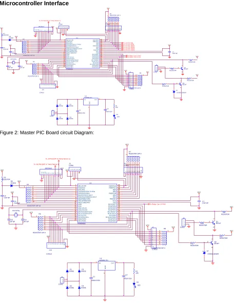
Temp Sensor Signal Conditioning Circuit
J8 O/P Con
1 2
U5-LM35
LM35
2
3 1
GN
D VOUT
+5V
J9 +5V Cons Voltage
1 2 J7 +5V Cons Current
1 2
J14 +5V 1 2
U3-LM35
LM35
2
3 1
GN
D VOUT
+5V
U9-LM35
LM35
2
3 1
GN
D VOUT
+5V
U4-LM358
LM358 4
7 5 1
2
6 3
8
-VCC
Output B
Non Inv I/P B Output A
Inv I/P A
Inv I/P B Non Inv I/P A
VCC
R9 POT
1 3
2
R19 RESISTOR R10 RESISTOR
J15 O/P Con
1 2 R12 RESISTOR
5. SOFTWARE DEVELOPMENT
The application software for the total system consists of master slave modules, the code for the PIC-microcontroller master temperature monitor and control and the slave for analog to digital conversation of the received voltage and serial transmission to generate the necessary plots on computer. The slave is also designed to generate various user required waveforms. The software at the PC end providing the user interface, and also the protocol for communication between the PC and the Master and slave microcontroller unit.
ALGORITHM
1. Start.2. Handshaking initialization (ctrl + A).
3. Input range for temperature controlling via serially. 4. Increase temperature of temperature sensor. 5. Continuously compare temperature ranges.
6. if(adc_val > l value && adc_val < U_value).Then SET temperature, Voltage, current relays ON.
7. Else SET them OFF.
8. Transmit both voltages and current value via serially 9. Plot the respective graphs on VB.
10. Generate the readings table using VB.
Waveforms generated
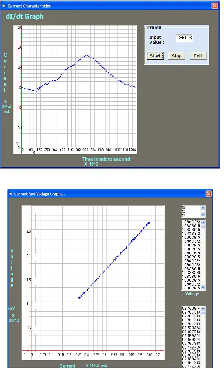
Table 1: Current and Voltages for temperature range between 31ºC to 61°C.
7. CONCLUSION
An electrical/ electronic temperature switching analyzer has been developed for obtaining the I-V characteristics of temperature sensing electronic devices. This unit has additional feature to generate different types of excitation waveforms such as triangular ramp, step, etc., with single or multiple cycles and programmable sweep rate. This protocol will be a complete solution for an application development electronic industry for testing the electronic device under various temperature conditions and variable waveform input.
8. REFERENCES
1. Chitters Nagaraja Murti, Sharma Ramgopal, S. Ashokan, “Simple Low Cost Electrical Switching Analyzer for I-V Characterization of Switching Samples And Devices” IEEE transaction on Instrumentation and Measurement, Vol, 55, No.1, February 2006, pp-248-256. 2. PIC16F877 Data Sheet by Microchip.
3. National semi-conductors data sheets.