Growth and Dielectric Properties of SnSe
0.5Te
0.5Crystals
Solanki G.K.*1, Patel K.D.1, Gosai N.N.1,2 and Patel Rahul B.11
Department of Physics, Sardar Patel University, Vallabh Vidyanagar 388 120, Gujarat, INDIA
2Faculty of Technology, Marwadi Education Foundations Group of Institutions Rajkot, Gujarat, INDIA
Available online at: www.isca.in
Received 28th May 2012, revised 31st May 2012, accepted 7th June 2012
Abstract
The present paper reports the growth of SnSe0.5Te0.5 single crystals by direct vapor transport technique (DVT) using two zone
horizontal furnace. Detailed growth parameters for these crystals are reported here like temperature profile, ampoules dimension and furnace dimension etc. The as grown crystals were used for dielectric measurements in the frequency range 200 Hz to 1 MHz using LCR meter model HP 4284A in temperature range 303 K to 523 K at applied magnetic field of 1 kG, 2 kG and 3 kG. The dielectric properties i.e. capacitance (C), alternating current conductivity (σac), dielectric constant (ε’), dielectric loss tanδ and imaginary dielectric constant (ε’’) are measured and represented as a function of frequency and temperature.
Keywords: SnSe0.5Te0.5 crystals, vapor transport technique, dielectric constant and a.c. conductivity.
Introduction
Recently, the physical properties of such type of layered materials have been a field of intensive study. And due to their electrical and optical properties, the binary IV- VI layered semiconducting compounds produced a great deal of interest and applications in different fields. An interesting group of compounds which has received increasing attention from the fundamental as well as the industrial or application point of view. The IV– VI compounds have been the subject of considerable attention, owing to their technological importance in the IR field. In addition, their unusual characteristics make them a preferred subject for solid state basic research. The fabrication of devices with alloys of these compounds with photo detection and injection laser capabilities has been an important recent technological development1. Owing to its various physical, mechanical and electronic properties of semiconductor material can be used for semiconductor device application. It can also be used on polycarbonate (PC) in outdoor applications, the coating protects PC from solar radiation and decreases the oxidation rate and photo-yellowing of PC. Particularly, ZnO nanowires can be used in dye sensitized solar cells and in field emission devices. It also has potential applications in laser diodes and light emitting diodes (LEDS)2.
In the photo catalytic reactions, the semi conducting material absorbs light energy more than or equal to energy gap, which generates the holes and electrons, which further give rise to efficient oxidizers of organic dyes3. To conversion of solar energy into electrical energy in photogalvanic cell through redox reaction because solar energy is currently high on absolute costs compared to other sources of power such as non – renewable sources. The photogalvanic cell was used as a
converter device which converts solar energy (photon) in to electrical energy.
In present work i.e. dielectric properties of solids often gives good insight into the electric field distribution within the solids. Studying the dielectric constant as a function of frequency and temperature, the various polarization mechanisms in solids can be understood. It attracts attention in infrared optoelectronic devices, radiation detectors, holographic recording system, electrical switching, polarity dependent memory switching and solar cell fabrication.
The study of dielectric behavior of chalcogenide materials can be useful for the understanding of conduction mechanism. In addition, a study of temperature dependence of dielectric permittivity particularly in the range of frequencies where dielectric dispersion occurs can be of great importance for the understanding of the nature and origin of the losses occurring in these materials4. SnSe0.5Te0.5 chalcogenides are known to possess the orthorhombic structure having anisotropic nature in their physical and electrical properties5. SnSe0.5Te0.5, being a member of this family, is less investigated as far as its dielectric properties are concerned.
Material and Methods
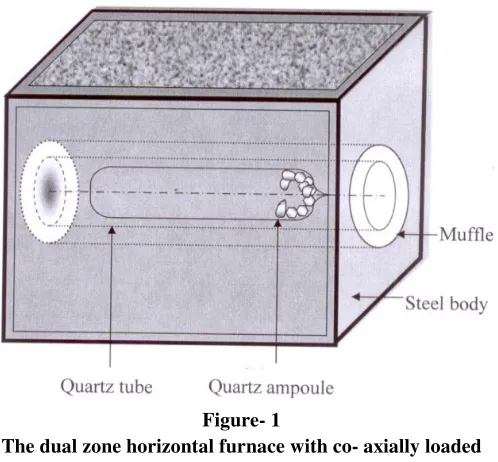
Crystal Growth: In the present investigations SnSe0.5Te0.5 crystals have been grown by using direct vapor transport (DVT) technique. For the growth of the crystals, two zone horizontal furnace having required dimensions has been used as shown in figure 1. The furnace was constructed by a special sillimanite threaded tube closed at one end, 450 mm in length, 70 mm outer diameter, 56 mm inner diameter with threaded pitch of 3 mm, imported form from koppers fabriken feuerfester, Germany. High quality quartz ampoules were used for growth experiment having dimensions of 24 cm length, 2.4 cm outer diameter and 2.2 cm inner diameter.
High quality chemically cleaned quartz ampoule was filled with stoichiometric proportion of pure Sn (99.999%), Se (99.99%) and Te (99.99 %) of about 10gm then it was sealed under pressure of 10-5 Torr. The sealed ampoule was kept in two- zone horizontal furnace. The temperatures of both the zones were slowly but gradually raised upto desired temperature and maintained that temperature for specific time, after that furnace was cooled off at the room temperature. Table 1 shows the detailed growth conditions for SnSe0.5Te0.5 single crystal. The ampoule was broken and shaken well with help of agate mortar to prepare fine powder of this compound. Full detailed analysis of growth of SnSe0.5Te0.5 single crystal/ compound has been presented in our earlier published paper8.
Figure- 1
The dual zone horizontal furnace with co- axially loaded ampoule
High temperature LCR measurement set up: Figure 2 shows high temperature LCR experiment set up used for current investigation. The as grown crystals or pallets may be used directly for dielectric study. The geometrical dimension of used sample was measured by a travelling microscope and the
thickness has been measured by micrometer screw. The dielectric measurements were carried out using two standard electrode method. The specimen was mounted in between two flat stainless steel parallel electrodes of a specially designed sample holder. Both the upper and lower base of the holder can be screwed in four proper contact of the sample with the electrode. The sample holder was enclosed in a specially built resistance heating furnace which is capable to provide temperature up to 625 K. We have measured dielectric parameters automation and controlling software ‘LABVIEW’ is used. The parameters like the thickness and area of the sample, starting and ending temperature and frequency have been set in software. These input data are essential in order to measure the dielectric properties at desired temperature and frequencies. The digital temperature controller DT84848 is used to monitor the preferred temperature of the specimen. When preferred temperature is achieved HP4284A LCR meter will scan all the frequencies and resultant data is stored in the storage device.
Results and Discussion
The grown crystals possess orthorhombic structure having lattice parameters as a= 6.3 A0, b= 9.2A0 and c= 10.1A0 measured using XRD spectra8. The capacitance, dielectric constant and dielectric loss are important parameters in the selection of materials for device application. The dielectric constant ε’ is evaluated from the equation,
C = ε’ ε0 A / d (1)
where C is the capacitance of the crystalline sample (F), d is the thickness of the sample (m), ε0 is the permittivity of free space
(ε0 = 8.85 × 10⁻¹² F m−1) and A is the area of the cross section of
sample (m2).
The imaginary part of the dielectric loss (ε’’) at the various
frequencies was calculated using the measured conductance values (G) from the relation,
ε’’ = d G / A ε0 w (2)
where G is the dc conductance of the sample, and ω (= 2πf) is
the angular frequency. The dielectric loss tan δ was calculated
from the relation,
tan δ = ε” / ε’ (3)
The alternating current (ac) conductivity σac is calculated using
the relation,
σac = 2 π f ε0 ε’ tan δ (4)
Table-1
Growth condition for SnSe0.5Te0.5 single crystals
Crystal Temperature
gradient in furnace
∆T (K)
Time for which ampoule was kept in temperature
gradient (Hours)
Size of the crystals (cm2)
Thickness of the crystals (µm)
SnSe0.5Te0.5 1003- 953 168 0.4 × 0.5 40
Figure-2
High temperature LCR experiment set up
Figure-3
Variation of Capacitance with frequency and temperature 0.0E+00
5.0E-11 1.0E-10 1.5E-10 2.0E-10
0.0E+00 2.0E+05 4.0E+05 6.0E+05 8.0E+05 1.0E+06 1.2E+06
C
a
p
a
c
it
a
n
c
e
C
(
F
a
ra
d
)
Frequency F (Hz)
T=303K
T=353K
T=403K
T=453K
T=503K
Figure-4
Variation of dielectric loss with frequency and temperature
Figure-5
Variation of dielectric constant with frequency and temperature
Figure- 6
Variation of a. c. resistivity with frequency and temperature 0.0
0.5 1.0 1.5 2.0 2.5 3.0
0.0E+00 2.0E+05 4.0E+05 6.0E+05 8.0E+05 1.0E+06 1.2E+06
D
ie
le
c
tr
ic
l
o
s
s
(
ta
n
δ
)
Frequency F (Hz)
T=303K
T=353K
T=403K
T=453K
T=503K
T=523K
0 300 600 900 1200
0.00E+00 2.50E+05 5.00E+05 7.50E+05 1.00E+06
D
ie
le
c
tr
ic
C
o
n
s
ta
n
t
(
ε
')
Frequency F (Hz)
T=303K
T=353K
T=403K
T=453K
T=503K
T=523K
0 30000 60000 90000 120000
0.00E+00 4.00E+05 8.00E+05 1.20E+06
a
.c
.
R
e
s
it
iv
it
y
(
Ω
c
m
)
Frequency F (Hz)
T=303K
T=353K
T=403K
T=453K
T=503K
Figure-7
Variation of Real part of dielectric constant with frequency and temperature
Figure-8
Variation of imaginary part of dielectric constant with frequency and temperature
As one can see that dielectric behavior is frequency dependant as well as temperature dependent. The capacitance is decreases with temperature and it decreases with increasing frequency for SnSe0.5Te0.5 crystals as shown in figure 3. Because at lower temperature the mobility of ions is very low and so is the conductivity, resulting a lower value of capacitance. With temperature, the mobility of charge carriers increases, resulting the increase in space charge polarization and capacitance both.
Figure 4 shows variation of dielectric loss with frequency at different temperature. Dielectric loss tanδ, decreases with
increasing frequency and it increases consistently with temperature for SnSe0.5Te0.5 crystals. For many materials it has been observed that the dielectric loss decreases as frequency increases9,10. The response of the normal materials to applied fields depends on the frequency of the applied fields. In fact, polarization of material does not respond instantaneously to an applied field so the permittivity is often treated as a complex function of frequency. The dielectric nature of single crystals of L- Histidinium Trifluoroacetate prove that the sample has low dielectric constant and dielectric loss values at high frequency11.
From figure 5, dielectric constant is observed to be high at lower frequency and it systematically decreases with increasing frequency up to 600 kHz and then after it nearly becomes frequency independent for these grown crystals. The dielectric constant of solids is known to consist of contribution from electronic, ionic, dipolar and space charge polarization exhibits itself prominently at lower frequency. This polarization is known to arise from defects or impurities present, grain boundaries etc12,13 and also due to creation and distribution of dipoles either within the bulk or at the surface of the crystals. Hence the higher values of the dielectric constant at lower frequency in the present investigation may be because of a large amount of space charge polarization14-16.
Less frequency dependence value of ε’ is taken as static
dielectric constant. This indicates the probable presence of ionic and electric polarization, since the concentration of crystals defects controlling the space charge polarization negligible. The dispersion of ε’ with frequency can be attributed to the
Maxwell- Wagner type interfacial polarization i.e. the fact that in homogeneities give rise to a frequency dependence of 0
200 400 600 800 1000 1200
0.00E+00 3.00E+05 6.00E+05 9.00E+05 1.20E+06
R
e
a
p
a
rt
o
f
D
ic
lc
tr
ic
c
o
n
s
ta
n
t
(E
')
Frequency F (Hz)
T=303K T=353K T=403K T=453K T=503K T=523K
0 500 1000 1500 2000
0.0E+00 3.0E+05 6.0E+05 9.0E+05 1.2E+06
Im
a
g
in
a
ry
p
a
rt
o
f
D
ic
lc
tr
ic
c
o
n
s
ta
n
t
(E
")
Frequency F (Hz)
T=523K
T=503K
T=453K
T=403K
T=353K
conductivity because charge carriers accumulate at the boundaries of less conducting regions, thereby creating interfacial polarization.
The temperature is also found to exhibit an interesting influence on the dielectric properties. The value of ε’ decreases with
temperature for the grown compound/ sample. From the fig. one can notice that at low temperatures the variation in dielectric constant is much less frequency dependant, while at higher temperatures the increment in dielectric constant is stronger and much more frequency dependant. This is due to lattice expansion, polarizability of the constituent ions due to increase of atomic polarizability17. The changes in ε’ with temperature
are of similar nature at all the frequencies.
The conductivity of SnSe0.5Te0.5 crystals is increases with temperature and frequency both while at higher frequency it is much more independent of frequency with compared to that lower frequency range. The resistivity decreases with frequency and temperature both with can be seen from figure 6. So at higher temperature SnSe0.5Te0.5 single crystals become more conducting so its resistivity decreases with temperature. At lower frequency the increase in conductivity is more rapid and at higher frequency the conductivity increases very slowly.
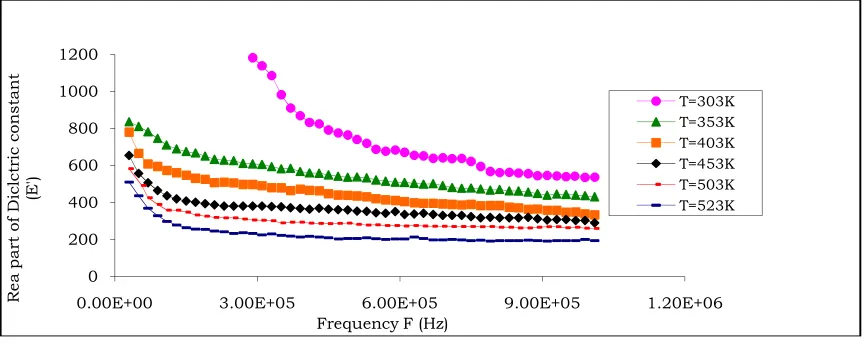
Figure 7 shows variation of real part of dielectric constant with frequency. The change in complex/ imaginary part of dielectric constant with frequency is shown in figure 8 and indicates that as the frequency increases the value of imaginary part of the dielectric constant decreases. And also it decreases with temperature for SnSe0.5Te0.5 crystals. The observed decrease in
ε’’ values with frequency and decrease in ε’’ with temperature,
which are the common features of many/ other compositions and it can be on explained on similar arguments as for dielectric constant ε’.
Conclusion
Here we have been grown successfully SnSe0.5Te0.5 single crystals using direct vapor transporting technique having fairly large dimension such that these crystals is used for device application as well as for characterization purpose. The dielectric properties i.e. capacitance (C), alternating current conductivity (σac), dielectric constant (ε’), dielectric loss tanδ
and imaginary dielectric constant (ε’’) are measured and
represented as a function of frequency and temperature.
Acknowledgement
Authors are thankful to UGC, New Delhi, India for the sanctioned of a major research project to G. K. Solanki which provided the necessary financial help for carrying out this work.
References
1. Barote Maqbul A., Yadav Abhijit A., Surywanshi Rangrao V., Deshmukh Lalasaheb P., Masumdar Elahipasha U,
Chemical Bath Deposited PbSe Thin Films: Optical and Electrical Transport Properties, Research Journal of Chemical Sciences, 2(1), 15-19 (2012)
2. Ezenwa I.A., Synthesis and Optical Characterization of Zinc Oxide Thin Film, Research Journal of Chemical Sciences, 2(3), 26-30, (2012)
3. Santhanalakshmi J. and Komalavalli R., Visible Light Induced Photocatalytic Degradation of some Textile Dyes Using Silver Nano Particles, Research Journal of Chemical Sciences, 2(4), 64-67 (2012)
4. Sharma J., Kumar S., Role of Pb additives in the dielectric properties of Se90In10 and Se75In25 glassy alloys, Journal of Ovonic Research, 6(1), 35- 44 (2010)
5. JCPDS file, PDF- 2 No.35-1042
6. Wu X., Yang E.S. and Evans H.L., Negative capacitance at metal‐ semiconductor interfaces, J. Appl. Phys, 68, 2845, (1990)
7. Champness C.H. and Clark W.R., Anomalous inductive effect in selenium schottky diodes, Appl. Phys. Lett., 56, 1104 (1990)
8. Solanki G.K., Patel K.D., Patel Rahul B., Unadkat Sandip, Patel Dipika B. and Gosai N.N., Synthesis of GeTe0.1Se0.9 single crystals and its structural and optical characterization, Journal of Optoelectronics and Biomedical Materials, 2(3), 99-107 (2010)
9. Parekh B.B. and Joshi M.J., Growth and characterization of gel grown calcium pyrophosphate tetrahydrate crystals, Cryst. Res and Technol., 42, 127–129 (2007)
10. Parekh B.B., Vyas P.M., Vasant Sonal R. and Joshi M.J., Thermal, FT–IR and dielectric studies of gel grown sodium oxalate single crystals, Bull. Mater Sci., 31, 143- 147 (2008)
11. Suresh S., Optical and Dielectric Properties of L-Histidinium Trifluoroacetate NLO Single Crystal, Research Journal of Chemical Sciences, 2(2), 83-86 (2012)
12. Maxwell J.C., Electricity and Magnetism, New York: Oxford Uni. Press, 1, 828 (1973)
13. Wagner K.W., Am. Phys., 40, 817 (1973)
14. Rao K.V. and Smakula A., Dielectric properties of Ailaline earth fluoride single crystals, J. Appl. Phys., 37, 319 - 321 (1966)
15. Reddy Y.R. and Sirdeshmukh L., Dielectric properties of NaIO4 and KIO4, Solid State Comm., 40, 353–356 (1981)
16. Sastry S.S., Satyanandam G., Subrahmanyan A. and Murthy V.R.K., Dielectric properties of HgCl2:2KCl:H2O single crystals in the radio frequency region, Phys. Stat. Solidi, 105, K71 (1988)