OPTIMIZATION OF ION IMPLANTATION USING TRIM SOFTWARE FOR THE
FORMATION OF SHALLOW N
+/P JUNCTION IN GERMANIUM SUBSTRATE
Umar Abdul Aziz
1,a, Nur Farhana Arissa
1,b, Siti Rahmah Aid
1,c,,Hafizal Yahaya
1,d, Anthony Centeno
1,e,
Satoru Matsumoto
1,f, Akira Uedono
2,g, David McPhail
3,h1 Malaysia-Japan International Institute of Technology, Universiti Teknologi Malaysia, Jalan Sultan Yahya
Petra, 54100 Kuala Lumpur, Malaysia
2 Faculty of Pure and Applied Science, University of Tsukuba, Tsukuba, Ibaraki 305-8573, Japan
3 Department of Material, Imperial College London, SW72AZ, England, United Kingdom
a[email protected], b[email protected], c[email protected] (corresponding author),
d [email protected], e[email protected], f[email protected], g[email protected],
ABSTRACT
Silicon (Si) device down-scaling is facing a big challenge to maintain its high drive current capability along with lower leakage current. Due to its similarities with Si, the interest has been focused on Germanium (Ge) as a substitute for device substrate. However, there are major problems in fabricating complementary metal-oxide semiconductor (CMOS) devices i.e. poor dopant solubility, low dopant activation and large dopant diffusion coefficient. These required further optimization on fabrication parameters involving ion implantation process. This paper reports the optimization of ion implantation parameters such as energy and dose. Co-implantation technique employing two atoms with different size will be adopted for forming the shallow
n+/p junction in Ge. The stress associated with atomic size is
expected to be introduced into the Ge lattice. This stress will be manipulated to enhance dopant activation while controlling the diffusion. Low energy of dopant-ion implantation is selected to achieve high dopant concentration near the surface. The simulation parameters of two atoms were arranged to get such result where the effect of stress from co-implantation process can be manipulated.
Keywords — co-implantation, dopant distribution, amorphous layer, defect vacancies, germanium, np junction
1. INTRODUCTION
According to the International Technology Roadmap for Semiconductors (ITRS) 2010, it is reported that the traditional scaling of planar Si-CMOS devices is becoming difficult due to the physical limit in down-scaling dimension. Germanium (Ge) and III-V compound have been pointed out as a new material candidate for pMOS and nMOS devices,
respectively. This is due to the material properties that could improve the density, energy efficiency and reliability of the devices. However, the utilization of the same material for both nMOS and pMOS devices is important in order to reduce the process complexity and cost in manufacturing process. The interest has been focused on Ge due to similarities with Si and its higher carrier mobility (i.e. two times higher mobility for electrons and four times for holes compare to Si) [1–5].
One of the process involve in manufacturing CMOS devices is the fabrication of the pn junction. Two major processes that will be employed in the fabrication of pn junction are ion implantation and thermal annealing. However, unlike Si, there are many problems related to the dopant electrical activation and diffusion behaviour in Ge substrate during the fabrication process [5-9]. Since dopant activation and diffusion are controlled by the interactions between dopant and defects, it is important to control the defects introduced in the substrate by ion-implantation process. Aggressive change or uncontrollable processing parameter can enhance these dopant-defect interactions which result in anomalous characteristics of the devices.
Previous studies have revealed that fabrication of nMOS is facing severe problem compare with pMOS [9]. This is due to the heavy dopant ions i.e. arsenics (As) or antimony (Sb) is widely used for n-type dopant ion implantation results in more damages/defects. Furthermore, Ge easily forms unstable oxide on the surface which also can induce defects into the substrate [10]. Consequently, these damages/defects give substantial effect on the dopant electrical activation and diffusion during the thermal annealing process. Therefore, it is important to select appropriate atoms and process parameter to reduce the damages/defects introduced by ion-implantation during the formation of n+/p junction.
stress associated with atomic size will be introduced into the Ge lattice which subsequently contributes to the enhancement of dopant activation level [11]. Therefore, in regard to this background, this study will demonstrate the optimization of ion-implantation parameters by adopting co-implantation technique. The optimization will be done by varying the ion implantation process parameters i.e. ion implantation energy and dose concentration using Transport of Ion in Matter (TRIM) software. The finding of the optimization will also be discussed.
2. EXPERIMENTAL DETAILS
The co-implantation process was consisted of the crystalline Ge substrate that was ion implanted with two different sizes of atoms. Tilt angle of 7o was selected to minimize the
channelling effect [12-13]. This process was modelled using the ion implantation software of TRIM. TRIM is Monte Carlo computer program that calculates the interactions of energetic ions with target. It consists of a group of programs called Stopping and Range of Ion in Matter (SRIM); which calculate the stopping and range of ions into matter using a quantum mechanical treatment of ion-atom collisions [14].
Phosphorus, P (atomic radius of 98 pm) and tin, Sn (atomic radius of 145 pm) were selected as a dopant and non-dopant atoms, respectively. P was selected as an n-type dopant due to its light properties. The simulations were firstly performed by varying the implantation energy and dose concentration of dopant atom (i.e. P atom). Low energy at the series of 20 keV, 30 keV, and 40 keV were selected in order to form a shallow junction. Dose concentration was varied between 3.0E14 – 6.0E14 cm-2 to achieve maximum dopant
concentration level of 1E20 cm-3 [11]. Ion projected ranges
(Rp) of P were simulated using SRIM. The simulation of non-dopant ion (i.e. Sn) was then performed based of the results of dopant TRIM simulation. The implantation energies of Sn were adjusted so that the projected range of Sn ion implantation will be similar to those of P ion implantation. Dose concentrations of Sn were then manipulated to achieve maximum dopant concentration level of 1E20 cm3 [11].
From TRIM simulation of both ions, damage event for vacancies were observed and raw data from TRIM simulation were analyzed to get information related to the damage layer and concentrations.
3. RESULTS AND DISCUSSION
Table 1 shows projected ranges and ion implantation energy of P and Sn co-implantation calculated from SRIM simulation. Projected ranges of Sn were manipulated by varying the implantation energy so that it will be similar to those of P. It is important to overlap the profile to fully utilize the effect of stress associated with atomic size. From Table 1, it is found that the projected range, Rp for P and Sn are between 210 – 438 Å. It is also confirmed that the projected range increased with implantation energy.
Table 1 Projected range, Rp and co-implantation energy of P and Sn ions
P
Implantation Rp
Sn
Implantation Rp
20 keV 210Å 58 keV 238Å
30 keV 310 Å 90keV 310Å
40 keV 400Å 130keV 438Å
(a)
(b)
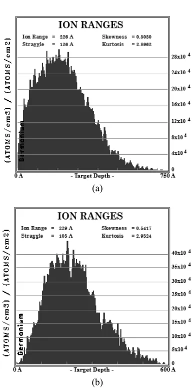
Figure 1 shows the TRIM simulation results of ion range distribution for the 20-keV P ion implantation and 58-keV Sn ion implantation. Projected ranges calculated from this profile are in a good agreement with those of SRIM calculation; with calculation error of ±10%. The same results were also obtained for (30-keV P/90-keV Sn) and (40-keV P/130-keV Sn) profiles.
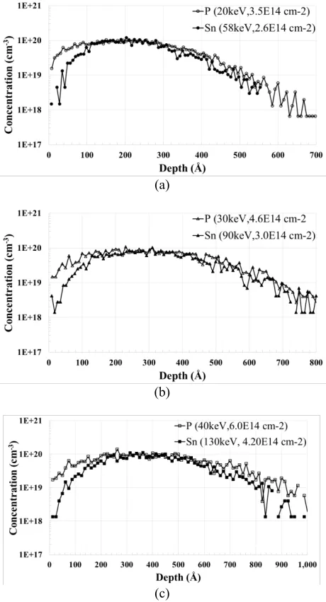
Dopant ion concentration profiles can be achieved by multiplying the ion range results of Figure 1 with the implantation dose. Implantation dose were manipulated to achieve maximum dopant concentration of 1E20 cm-3. The
calculation was performed using Equation (1). The result is shown in Figure 2 and Table 2.
(a)
(b)
(c)
Figure 2 Dopant distribution profile for co-implantation in Ge by the combination of (a) P: 20 keV/ Sn: 58 keV (b) P: 30 keV/ Sn: 90 keV (c) P: 40 keV/ Sn: 130 keV
Impurity Concentration (Atoms/cm3)
= Ion Distribution Profile (Atoms/cm3) / (Atoms/cm2)
× Implantation Dose (Atoms/cm2) Eq. (1)
From these results, it is shown that the dose concentration for each parameter needs to be varied from 2.6E14 cm-2 –
6.0E14 cm-2 in order to achieve similar maximum dopant
profile of 1E20 cm-3. It is also confirmed that dose
concentration increased with implantation energy. It is due to implantation of higher energy will result in the deeper profile. Consequently, higher dose concentration is required in order to occupy the lattice site to the deeper range.
Table 2 Dose concentration for P and Sn co-implantation
P (keV) Dose (cm-2)
Sn (keV) Dose (cm-2)
20 3.5E14 58 2.6E14
30 4.0E14 90 3.0E14
40 6.0E14 130 4.2E14
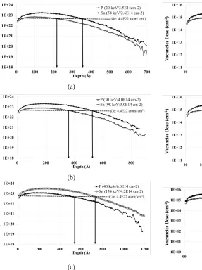
As previously stated, damages and defects will be introduced into the substrate during the ion implantation process. Figure 3 shows the damage layer (i.e. amorphous layer) created during the ion-implantation process. It is assumed that the amorphous layer was produced when the displacement atom density (vacancies concentration) exceeds the single-crystal’s atomic density of Ge (i.e., 4.4E22 atom/cm3). The
calculation was performed using Equation (2). From the results, the depth of amorphous layer varied from 218 – 738 Å. The depth is increased with the energy as higher implantation energy results in more damage to the target substrate. The same tendency can also be observed from the damage concentration shown in Figure 4. The calculation for damage concentration was performed using Equation (3). The results for these calculations were summarized in Table 3 and 4.
Vacancy Concentration (vacancy/cm3)
= Vacancy Dose (Vacancy/ Å-cm2) / 108 Å Eq. (2)
Defect Dose (cm-2)
(a)
(b)
(c)
Figure 3 Amorphous layer created by P and Sn
co-implantation in Ge with energy of (a) P: 20 keV/ Sn: 58keV (b) P: 30keV/ Sn: 90KeV (c) P: 40 keV/ Sn: 130 keV
Table 3 Amorphous layer of P and Sn co-implantation in Ge
P (keV)
Amorphous layer (Å)
Sn (keV)
Amorphous layer (Å)
20 218 58 357
30 380 90 525
40 538 130 738
(a)
(b)
(c)
Figure 4 Defects vacancies dose distribution of P and Sn implantation in Ge with energy of (a) P: 20 keV/ Sn: 58keV (b) P: 30keV/ Sn: 90KeV (c) P: 40 keV/ Sn: 130 keV
Table 4 Peak vacancies dose concentration for P and Sn co-implantation in Ge
P
(keV) Dose (cm
-2) Sn (keV) Dose(cm-2)
20 8.72E14 58 2.19E15
30 1.15E15 90 2.66E15
40 1.55E15 130 4.04E15
4. SUMMARY
The optimization of ion implantation parameter for the formation of shallow n+/p junction in Ge substrate was
expected to be introduced into the Ge lattice during the co-implantation process. Ion co-implantation parameters such as energy and dose were varied in order to attain an overlap profile of P and Sn with maximum dopant concentration of 1E20 cm-3. This is important in order to fully utilize the effect
of stress for enhancing the dopant activation level while controlling the diffusion during the fabrication process.
5. ACKNOWLEDGEMENT
This work is supported by Imperial College Global Engagement Grant, Universiti Teknologi Malaysia International Networking Grant (PY/2015/04262), Ministry of Education, Malaysia and Universiti Teknologi Malaysia Research University Grant Scheme (PY/2014/03088; Vote No: 01K38).
6. REFERENCES
[1] ITRS 2010 Report at www.itrs.net
[2] H. Shang, M. M. Frank, E. P. Gusev, J. O. Chu, S. W. Bedell, K. W. Guarini, and M. Ieong, IBM J. Res. & Dev., vol. 50, pp.337 (2006)
[3] C. H. Lee,, T. Nishimura, T. Tabata, S. K. Wang, K. Nagashio, K. Kita, and A. Torium,IEDM 2010, pp. 18.1.1 (2010)
[4] E. Simoen, and J. Vanhellemont, J. Appl. Phys., vol. 106, pp. 103516 (2009)
[5] K. Kakushima, R. Yoshihara, K.Tsutsui, and H. Iwai, Ext. Abs. the 13th Int. Workshop on Junction Technology 2013, pp. S3-3(L.N.) (2013)
[6] G. Thareja, J. Liang, S. Chopra, B. Adams, N. Patil, S. L. Cheng, A. Nainani, E. Tasyurek, Y. Kim, S. Moffatt, R. Brennan, J.McVittie, T. Kamins, K. Saraswat, and Y. Nishi, IEDM 2010, pp. 10.5.1 (2010)
[7] S. Takagi, T. Tezuka, T. Irisawa, S. Nakaharai, T. Numata, K. Usuda, N. Sugiyama, M. Shichijo, R. Nakane, and S. Sugahara,Solid-State Electron., vol. 51, pp. 526 (2007)
[8] S. Mirabella, D. De Salvador, E. Napolitani, E. Bruno, and F. Priolo, J. Appl. Phys. , vol. 113, pp. 031101 (2013) [9] E. Simoen, A. Satta, A. D’Amore, T. Janssens, T. Clarysse, K. Martens, B. De Jaeger, A. Benedetti, I. Hoflijk, B. Brijs, M.Meuris, and W. Vandervorst, Mater. Sci. Semicond. Process, vol. 9, pp. 634 (2006)
[10] J. W. Oh and J. C. Campbell, J. Electron. Mat., vol. 33 (4), pp. 364 (2004)
[11] Jeehwan Kim et. al. Applied Physics Letters.,Vol 98, pp082112 (2011)
[12] Chi On Chui,a Leonard Kulig, Jean Moran, and Wilman Tsai, Appl. Phys. Lett., vol. 87 pp. 09190 (2005)
[13] N. Ioannou, D. Skarlatos, C. Tsamis,C. A. Krontiras, S. N. Georga, A. Christofi, and D. S. McPhail, Appl. Phys. Lett., vol. 93, pp. 101910 (2008)