1971
Non-Linear ADC using Multiphase Clock TDC
Mahantesh Mattada, Hansraj Guhilot
Abstract— This work presents Time based nonlinear ADC on FPGA platform. VCO is used external to the FPGA, for converting an input voltage to proportional time pulse. Then, a Counter TDC with Multiphase clock technique is implemented within the FPGA to convert time pulse into its digital equivalent. The overall ADC response has been approximated with second order exponential equation along with its coefficients has been presented here. Proposed 13bit nonlinear ADC with 77dB dynamic range by using only 2% of FPGA total resources makes it area efficient. Also sampling rate of 9.8ks/Seconds, acceptable nonlinearities, wide input range and dynamically reconfigurable structure are added advantages of the work.
Index Terms— TDC, Multiphase clock, Time based ADC, Non-Linear ADC, Logarithmic ADC, VCO based ADC.
—————————— ——————————
1 INTRODUCTION
Logarithmic Signal Processing is well known topic that exists in the field of communication engineering. Sometimes referred as companding or compression, it is a method used for dynamic signals. Logarithmic ADCs provide non-uniform quantization, helps in compression of analog input signal to its digital equivalent. i.e. In logarithmic ADCs, small analog input signal amplitudes are digitized with fine resolution, while large analog input signal amplitudes are digitized with coarse resolution. The well-known compression application is used for telephonic system. Other applications include a critical military radar system for electronic warfare, Instrumentation where compression of wide dynamic signals is required, Ultrasound/Sonar applications, Hearing aids and many other biomedical applications [1,2]. Recently logarithmic ADCs found as essential building blocks for pH readout system [3] brain machine interface [4] and sensor linearization [5]. The key advantage is to overcome bandwidth limitations in neural recording. Also, utilizing non-linear quantization to focus more on concentrated information in the time domain.
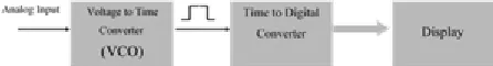
Traditional ADCs convert analog input into proportional digital value. But, working principle of time domain ADC, involving in converting analog input into a time pulse and then digitized into a digital code by using Time to Digital Converter (TDC). Since most of the low cost FPGAs do not have on-chip ADCs, the present architecture can be considered as a substitute for on-chip and on-board ADC. The present work provides reconfigurable, high resolution ADC, which stands high compared to on-board ADCs. The conceptual diagram of time based ADC is as shown in figure 1. Time based ADCs exhibit high resolution and conversion time directly proportional to input value. Also, ADCs based on time quantization alleviate drawbacks from voltage scaling, like nonlinearities and noise.
In the time-based ADCs architecture, time or frequency is quantized instead of voltage or current. A simplified block diagram of this ADC is shown in Fig 1. The input signal is in the voltage domain which is converted into time pulse by using a pulse width modulator or VCO circuit and then time signal is
quantized with a counter. A simple counter or an advanced TDC can be used for time quantization. In the present work TDC implemented on FPGA. TDC has application in any time measurement system and subsequently useful in industrial and research applications. The easiest topology of TDC is a Counter with enable input. There are different TDC topologies where resolution reached tens of picoseconds. In the present work we have adopted counter based TDC with a multiphase clock scheme to get optimal resolution.
Fig. 1Conceptual diagram of Time-based ADC
2 PRIOR ART
Many researchers have recently shown keen interest in time-based ADCs as there is a huge demand in low voltage applications. As a response to the new era of scaling CMOS technology numerous works published in recent years. A broad survey has been depicted in [6] covers almost all types of time-based ADCs. A method which is less complex and having component independent INL is Slope and Integrating ADC. But exhibit low sampling speed and low resolution. But researcher had overcome these drawbacks by replacing the counter by TDC in the architecture [7]. Another oldest ADC is Pulse width modulation (PWM) ADC [8], works with the same principle. Amplitude information is converted pulse width and then digitized by counter or advanced TDC. But, PWM suffers from signal distortion due to its nonlinear behaviour. Next, Asynchronous ADCs proposed in [9] known for dynamic power consumption. Voltage-controlled delay cell-based ADC proposed in [10], may suffer from high non-linearity. Another popular method is ADCs based on voltage-to-frequency conversion known as VCO based ADCs [11]. Our recent work on time-based ADC [12] include generating a single pulse proportional to input voltage and then converting pulse into its digital equivalent. Pulse shrinking TDC is incorporated for this purpose. But very few worked on time-based ADC on FPGA. One such work reported in [13] prototyped TDC and ADC on FPGA. The Scheme includes the ADC, which uses the ramping-comparing technique. Overall architecture uses a periodic logic levels shaped by passive RC
————————————————
Mahantesh Mattada is associated with Dept. of Electronics, Sanjay Ghodawat University, Kolhapur, India. He is currently pursuing PhD in electronics at VTU Belagavi, India. E-mail: [email protected]
Dr. Hansraj Guhilot (SMIEEE, FIETE) is currently associated with Dept. of Electronics, KC College of Engineering, Thane, India.
1972 (a)
(b)
Fig. 3 a) Counter TDC b) Counter TDC with PLL clock multiplier to enhance resolution
network and a Time to Digital Converter implemented for digitizing these pulses. Organization of the present work is illustrated as follows. Complete idea of the work is depicted in section III, Section IV illustrates design and implementation, section V illustrate about results and discussion. Finally, a brief conclusion given at the end.
3 PROPOSED WORK
Proposed work follows the technique of converting voltage information into proportional frequency using an external VCO. Processing this frequency information has been implemented within the FPGA. A simple version of TDC is used for this purpose. Finally, Digital output of the TDC will be displayed on seven segments. Following subsections will provide complete information of each block mentioned in figure1.
3.1 Analog input to Pulse Converter
Many commercial monolithic Phase Locked Loop (PLL) ICs available in the market. As they come up with built in Voltage Controlled Oscillator (VCO), one can use them for voltage to frequency conversion. In our work PLL IC565 has been used to get the advantage of the built-in VCO. The VCO output is connected to the FPGA, where one out of many pulses will be selected. A block is specially designed for this purpose within the FPGA. Since VCO is connected externally, dynamic configuration is also possible by varying RC constant. The variation of VCO output ‗ON‘ period with respect to applied input amplitude is measured and shown in figure2. Using nonlinear curve fitting technique, one can approximate the output behaviour of the circuit. Analog input is quantized to proportional time quantity. This involved in quantization error which is shown in the second part of figure2. Quantization error is obtained by calculating the difference between a best fit curve and actual readings. This quantization error will propagate till output, since the next stage TDC conversion is linear.
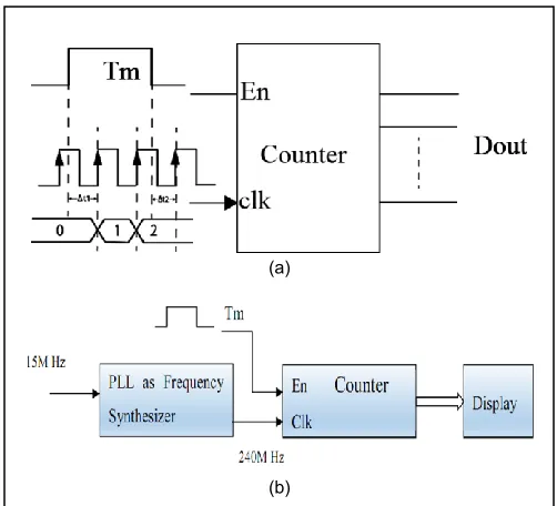
3.2 Time to Digital Converter
Several techniques of Time to digital conversion are available. However, counter based TDC has an advantage i.e. its dynamic range adjustability. By reducing the clock frequency, one can enhance the measurement range of the TDC. The resolution of the TDC is equal to the time period (TCLK) of the
clock. Due to bandwidth limitation, FPGA boards are equipped with low frequency crystal oscillators. To enhance
the resolution, one can utilize the PLL available within the
FPGA. Figure 3.b shows the diagram of Counter TDC with enhanced resolution by multiplying crystal clock frequency. As a specific case shown in fig.3, crystal clock 15MHz is multiplied by 16 using PLL, therefore resolution increases by
16 times i.e. 4.16ns.
The first limitation of the counter based TDC is its inherent quantization error. This is inevitable as the hit signal (Tm in fig3.) is asynchronous. If we consider both rising edge and falling edge errors, the total error may stretch to (but less than) 2*TCLK. Second, enhancement of resolution is not possible
when PLL reaches the upper limit. As a typical case PLL of Spartan3E FPGA has an upper limit of 300M Hz, beyond that it may produce undesirable output. However, earlier works [13,14] shown that, it is still possible to enhance the resolution beyond the clock period (TCLK). The technique adapted
familiarly known as multiphase clock method. Generating multiple phases of the same clock and identifying which phase of the clock is very close to hit signal. Consider the scenario as shown in fig.4, if a single-phase clock is used for measurement, the clk_0 would
be connected to counter creating a possible error. Consider the multiphase scenario where the clocks with phase shift of 90° are available to drive the counter. Considering the nearest rising edge clk_180 must drive the counter. An additional PLL required to obtain 4 phases of the clock. Successive stages will encode the information based on the selected phase information to attain high resolution. Separate fine measurement consisting of huge pipeline of flip-flops followed by encoding schemes makes the circuit bulky. The current work avoids this fine measurement block by directly selecting the appropriate phase of the clock to drive the counter. Overall block diagram of the proposed work is as shown in fig.5. The contribution of this work is the clock selector block. The added advantage of the present compared to earlier works lies in its simplicity of the design and area efficiency.
Fig. 2. Quantization of analog input to time pulse (T) and resultant Quantization error (TQe). 8Analog input vs ADC
1973
5 DESIGN AND IMPLEMENTATION
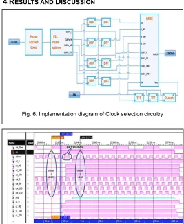
The system is designed and simulated using Xilinx 14.7 synthesis tool and tested its performance on SPARTAN 3E FPGA. The main components of the proposed design are VCO configured outside the FPGA, one on-chip PLL for frequency multiplication, one on-chip PLL with phase splitting feature, Clock selection circuitry and a Counter TDC.
Key block of the present work is clock selection circuitry and it is designed using flip flops, lathes and multiplexer circuits as shown in fig.6. This triggers the TDC with appropriate clock depends upon the occurrence of active edge of pulse input. The whole process will take nearly 3 clocks and these three pulses missed by the counter. To compensate this error, the counter is initialized to 3. If the hit signal is less than 3 TCLK,
still a provision is made in the system. Figure 7 shows switching of output clock i.e. clkout, from clk_270º to clk_90º. During the arrival of En (Hit) signal, clk_90º edge is close to the positive edge of En (pulse). Hence, the clock is switching to clk_90° from clk_270°, which is previously selected. Now, the maximum error factor ∆ at conversion is ¼TCLK period.
4 RESULTS AND DISCUSSION
Overall output response is as presented in figure 8. The mathematical model for the same is obtained using nonlinear regression. Looking into the curve one can conclude the overall system response is exponential. For simplicity one would try to fit using exponential function. With a curve fitting technique, we found the second order equation of the obtained curve and presented in equation 1.
𝐷𝑜𝑢𝑡(𝑣𝑖𝑛) = 𝛼𝑒 + 𝛾𝑒 (1)
Where α, β, γ and δ are the coefficients approximated while curve fitting and the values are given by 2562, 0.05923, 103.7 and 0.6884 respectively. However, to improve the
Fig. 4.The scenario of a multiphase clock based TDC [1]
Fig
.
5. Overall block diagram of proposed workFig. 8Analog input vs ADC output
Fig. 6. Implementation diagram of Clock selection circuitry
1974
nonlinearities, curve fitting using fifth order polynomial suggested and found better DNL and INL. Equation 2 depicts the final expression used to obtain DNL plot.
𝐷𝑁𝐿 = 𝐴𝑐𝑡𝑢𝑎𝑙 𝑠𝑡𝑒𝑝 𝑤𝑖𝑑𝑡ℎ − 𝐼𝑑𝑒𝑎𝑙 𝑠𝑡𝑒𝑝 𝑤𝑖𝑑𝑡ℎ 𝐷𝑁𝐿(𝐷𝑜𝑢𝑡) = 𝑀𝑒𝑎𝑠𝑢𝑟𝑒𝑑 𝐷𝑜𝑢𝑡 − 𝐷𝑜𝑢𝑡(𝑉𝑖𝑛)
𝐷𝑁𝐿(𝐷𝑜𝑢𝑡) = 𝑀𝑒𝑎𝑠𝑠𝑢𝑟𝑒𝑑 𝐷𝑜𝑢𝑡 − (𝛼𝑒 + 𝛾𝑒 ) (2)
Since, proposed ADC has high resolution, input noise could easily affect the nonlinearity. Hence, to improve nonlinearity spline smoothing is done. With smoothing parameter p equal to 0.99977941 and the specified weights wi, equation for spline
smoothing is given by equation 3.
𝑝 ∑ 𝑤(𝑦 − (𝑠𝑥)) + (1 − 𝑝)∫ ( ) 𝑑𝑥 (3)
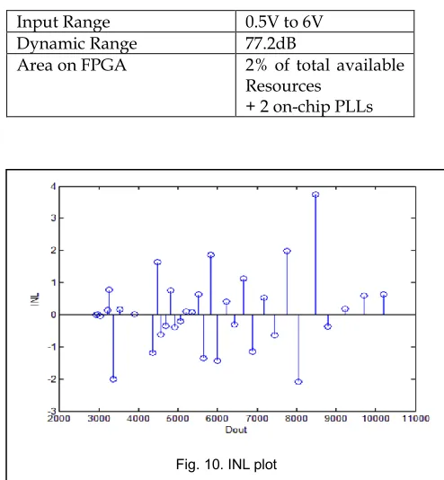
Resultant improvement in DNL is as depicted in figure 9. INL is the resultant cumulative sum of DNL, is also presented in figure 10. One more important parameter of ADC is dynamic range, given by
𝐷𝑦𝑛𝑎𝑚𝑖𝑐 𝑅𝑎𝑛𝑔𝑒 = 20𝑙𝑜𝑔 ( ) (4) However, present work needs an offset adjustment to get effective dynamic range. Calculations for the same proved 77dB effective dynamic range. Other parameters of proposed ADC are tabulated in Table1. Further improvement in the dynamic range and resolution can be dynamically attained by increasing the clock frequency of the TDC. One more advantage of time-based ADC is its inherent ability to maintain same conversion rate over different resolution and dynamic range. The conversion rate can only be altered by changing the time quantization in the VCO stage. In this project an external resistor and capacitor could able to change VCO free running frequency, thereby quantization level in time domain. Expression of free running frequency of the VCO is given by
𝐹𝑣𝑐𝑜 ≅ 𝐻𝑧 (5)
Table 1. Summary of the proposed ADC Parameters Non-linear ADC Type Exponential
Resolution 13bit
Maximum Conversion Rate 9.8Ks/S
Input Range 0.5V to 6V
Dynamic Range 77.2dB
Area on FPGA 2% of total available Resources
+ 2 on-chip PLLs
5
CONCLUSION
In this paper, we mentioned about many applications where, nonlinear ADC is an essential part of the system. The proposed nonlinear ADC fits in many such applications where, dynamic reconfiguration is often required. The multi-phase clock-based counter TDC is used for high accuracy measurement, thereby improved the resolution by 4 times. The ADC conversion time is proportional to input amplitude. Hence smaller input levels are quickly digitized. TDC based ADCs are promising future data converters, due to their high resolution, high dynamic range, small area and low power.
REFERENCES
[1] Guilherme J., Vital J. ―Logarithmic Analogue-to-Digital Converters‖ In: Rodríguez-Vázquez A., Medeiro F., Janssens E. (eds), CMOS Telecom Data Converters. Springer, Boston, MA [2] Yuwadee Sundarasaradula, Timothy G. Constandinou
and Apinunt Thanachayanont ―A 6-bit, Two-step, Successive Approximation Logarithmic ADC for Biomedical Applications‖, IEEE International conference, 978-1-5090-6113-6/16
[3] Apinunt Thanachayanont ―A 1-V, 330-nW, 6-Bit Current-Mode Logarithmic Cyclic ADC for ISFET-Based pH Digital Readout System‖, Circuits Syst Signal Process, 1 October 2014
[4] Mohsen Judy, Amir M. Sodagar, RezaLotfi and Mohamad Sawan ―Nonlinear Signal-Specific ADC for Efficient Neural Recording in Brain-Machine Interfaces‖, IEEE Transactions on Biomedical Circuits and Systems, Vol. 8, No. 3, June 2014
[5] Emilio Volpi, Nicolò Nizza, Paolo Bruschi ―A non linear ADC for sensor linearization‖ , IEEE PRIME Conference 2007
[6] Shahrzad Naraghi ―Time-Based Analog to Digital
Fig. 9. DNL plot
1975
Converters‖ PhD Dissertation, The University of Michigan, 2009
[7] E Delagnes, D. Breton, F. Lugiez, and R. Rahmanifard, ―A Low Power MultiChannel Single Ramp ADC With Up to 3.2 GHz Virtual Clock,‖ IEEE Transactions On Nuclear Science, vol. 54, no. 5, pp. 1735-1742, October 2007
[8] Analog Devices Data Conversion Handbook, http://analog.com/library/
analogDialogue/archives/39-06/data_conversion_handbook.html
[9] F. Akopyan, R.Manohar and A.B.Apsel, ―A Level-Crossing Flash Asynchronous Analog-to-Digital Converter,‖ Proceedings of the 12th IEEE International
Symposium on Asynchronous Circuits and
Systems(ASYNC), 2006
[10]H. Pekau, A. Yousif and J. W. Haslett, ―A CMOS Integrated Linear Voltage-to-Pulse-Delay-Time Converter for Time-Based Analog-to-Digital Converters,‖ ISCAS 2006, pp. 2373-2376.
[11]R. Naiknaware, H. Tang and T. S. Fiez, ―Time-Referenced Single-Path Multi-Bit Ʃ∆ ADC using a VCO-Based Quantizer,‖ IEEE Transactions on Circuits and Systems II, vol. 47, no. 7, pp. 596 – 602, July 2000
[12]Deepali Toraskar, Mahantesh P Mattada and Hansraj Guhilot ― Time based ADC using Pulse Shrinking TDC‖ IEEE I4C Conference Proceedings, 2016
[13]Jinyuan Wu, Sten Hansen and Zonghan Shi "ADC and TDC Implemented Using FPGA", IEEE Nuclear Science Symposium Conference Record, 2007