Jeyavijayan Rajendran,
Student Member, IEEE
, Ramesh Karri,
Member, IEEE
, James B. Wendt,
Member,
IEEE
, Miodrag Potkonjak,
Member, IEEE
, Nathan McDonald,
Member, IEEE
, Garrett S. Rose,
Member, IEEE
,
and Bryant Wysocki,
Member, IEEE
Abstract—Information security has emerged as an important system and application metric. Classical security solutions use algorithmic mechanisms that address a small subset of emerging security requirements, often at high energy and performance overhead. Further, emerging side channel and physical attacks can compromise classical security solutions. Hardware-based security solutions overcome many of the limitations of classical security while consuming less energy and improving performance. Nanoelectronics-based hardware security preserves all of these advantages while enabling conceptually new security mechanisms and security applications. This paper highlights nanoelectronics based security capabilities and challenges. The paper describes nanoelectronics-based hardware security primitives for device identification, digital forensics, and tamper detection. These primitives can be developed using the unique characteristics of emerging nanoelectronic devices such as complex device and system models, bidirectional operation, and temporal drift of state variables. We also identify important desiderata and outstanding challenges in nanoelectronics-based security.
Index Terms—Digital integrated circuits, hardware security, nanoelectronics, and memristors.
I. INTRODUCTION
Since the mid 1970s, information security has evolved from primarily focusing on the confidentiality and integrity of stored and in-transit data to incorporating trust, privacy, and remote ground truthing. Over this forty year span, the usage scenario of security technologies has evolved from securing physical premises with mainframe computers to securing lightweight, low-cost, high-performance, and low-power mobile phones, tablets, and sensors.
Classical security (i.e., mathematical or algorithmic) has created elegant security primitives and protocols. Unfortunately, these solutions are not only slow and consume significant amounts of energy for most modern applications but are also vulnerable to physical and side channel attacks (e.g., radiation or exposure to high temperatures). Classical and emerging security requirements and metrics may be addressed in superior ways using nanoelectronics.
Nanoelectronics enable conceptually new and strong security primitives and applications. Nanoelectronic security primitives create intrinsic feedback mechanisms that can provide security comparable to that offered by Shannon's diffusion and confusion principles while
subsuming these two fundamental principles as special cases. Nanoelectronic security primitives are potentially more robust than conventional complementary metal oxide semiconductor (CMOS) device-based security primitives. They can be the basis for provable security in an information theoretic sense as the complexity of compromising a nanoelectronics-based security primitive is equivalent to the hard problem of solving a large system of nonlinear equations. Finally, emerging, unconventional nanoelectronics have the potential to yield computing systems with miniscule form factors, ultra low-power consumption, and fast computation times relative to CMOS technologies.
A variety of materials and devices including memristors, graphene, plasmonics, and quantum dots are being investigated for use in nanoelectronics. These nanoelectronic devices have nonlinear input-output relationships and exhibit inherent process variations much like current CMOS technologies [1-5] while demonstrating technology specific characteristics.
Our objective is to qualitatively and quantitatively explain the security relevant capabilities of one such nanoelectronics technology, namely the memristor. In Section 2, we will explain why device nonlinear, bi-directional input-output characteristics, non-volatility, temporal drift, and unique device forming step are interesting from a security perspective. In Section 3, we describe how memristors can be used to build public physical unclonable functions, a security token that can be used in several cryptographic protocols. Section 4 explains how memristors can be used to generate random numbers. Section 5 explains how tamper evident memory and logic can be constructed using memristors. Section 6 concludes the paper. Overall, we expect to convey our vision of security, digital forensics, and tamper detection as important applications for nanoelectronics, specifically memristors.
II. NANOELECTRONICS AND NANOARCHITECTURES In recent years, device physicists have realized a wide variety of nanoelectronic devices. These include metal-oxide memristors, phase change devices, spin-torque transfer devices, carbon nanotubes, graphene, and quantum dots. We will show how security primitives can be built using some of the unique characteristics of metal-oxide memristors.
Nanoelectronic Solutions for Hardware
Security
A. Memristors 1) Theory
Leon Chua showed that memory resistance or memristance M(q) relates charge q and flux φ, such that the memristance of the device changes with the applied electric field and time [1]:
( ) ( ) . (1) M(q) is the memristance of a memristor, measured in ohms. Memristance at any time instance depends on the integrals of the voltage (current) across (through) the device from −∞ to that time. Thus, the memristor behaves like an ordinary resistor at any given instance of time, while its memristance depends on the history of the device [1,2].
2) Device structure
Memristive devices have been fabricated from a variety of materials. For example, a TiO2−x layer with oxygen vacancies on a TiO2 layer without oxygen vacancies sandwiched between metallic (platinum) electrodes as shown in Fig. 1(a) [2]. In another structure an insulator is sandwiched between two metal layers (metal-insulator-metal or MIM), where the insulating layer may be a variety of materials including chalcogenides [6,7], metal oxides [8,9], perovskites [10,11], or organic films [12,13]. 3) Operation
Memristors have at least two resistance states, a high resistance state (HRS) and a low resistance state (LRS). To switch a memristor from the HRS to the LRS (a SET operation), a voltage bias of the appropriate polarity and magnitude, VSET, must be applied to the device. A device
in the LRS may then be returned to the HRS (a RESET operation) by applying a lower voltage, VRESET. Additional
resistance states are attainable by limiting the applied voltage or current.
MIM memristors afford several switching styles depending on its material stack. When VSET and VRESET are
of opposite polarity, the device is said to be bipolar. When VSET and VRESET are of the same polarity, the device is said
to be unipolar. Nonpolar memristors demonstrate both bipolar and unipolar switching styles.
4) Simulation models
Memristor models for metal oxide and other device types have been developed based on their device physics [14]. The relation between the flux φ(t) and the memristance of the device, M(φ(t)), can be written as [14]:
( ( )) √( ( ) ), (2) where L, W and D are the length, width, and thickness of the device, respectively. η is ±1 depending on the polarity of the applied voltage, and µ is mobility of the dopants. The rate at which the domain wall moves is given as [42]
( ). (3)
where I is the current flowing through the memristor, and p is a fitting coefficient.
5) Characteristics
Metal-oxide memristor devices have unique characteristics that may be leveraged for security1.
1. Non-volatility: Memristors retain their memristance value even when the power is turned OFF.
2.Bi-directionality: Some bipolar memristors exhibit similar current-voltage characteristics irrespective of the polarity of the applied voltage or current. This is evident from the symmetric theoretical I-V curve in Fig. 1(b).
3.Non-linearity: The I-V characteristics of memristors are highly non-linear due to their time-dependent behavior, as shown in Equation 2. Also, the HRS to LRS ratio is typically on the order of 103-106.
4.Formation process: For many memristors, a separate forming step (Vf) is required to initialize the memristor to the LRS. Prior to this point, the memristor behaves as a linear resistor [15].
5.Memristance drift: On applying an input voltage (positive or negative) across certain metal-oxide memristors, the memristance changes because of the 1 All types of memristors do not possess all of these
characteristics. The specific characteristics exhibited by a memristor depend on the material used.
Pt
TiO2-X
TiO2
Pt
Vread
Vread
Vread
R
lo
ad
R
lo
ad
R
lo
ad
(a) (b) (c)
Fig. 2. Example polyominoes of size 1, 2, 3, and 4
movement of dopants, a process called memristance drift [2]. The amount of drift depends on the polarity, amplitude, and duration of the applied voltage.
6.Process variations: According to Equation 2, the memristance of a memristor is affected by process-variation induced changes in its dimensions and dopant concentration. Furthermore, the effects of variation in the thickness of the memristor upon its memristance values are highly non-linear (more significantly for the LRS than the HRS [16,17]).
7.Radiation-hardness: Some memristor devices are inherently radiation-hard due to their material properties [2].
8.Temperature stability: The LRS and HRS values are highly stable in the case of a TiO2 memristor since the temperature coefficient of resistance for TiO2 is very small (less than -3.82×10⁻³/K). However, the switching speed of the memristor varies with temperature because of the change in dopant atom mobility.
All of these characteristics with the exception of non-volatility and radiation-hardness pose problems when designing memory and logic circuits using a metal-oxide memristor. However, we show that these typically problematic characteristics can actually be useful in the context of security.
III. NANOELECTRONICS-BASED PUBLIC PHYSICAL UNCLONABLE FUNCTIONS (NANOPPUFS)
In this section, we introduce physical unclonable functions and public physical unclonable functions. We then describe the architecture of NanoPPUFs, analyze its security properties, and propose protocols that leverage NanoPPUFs. In this section, Alice and Bob want to exchange information securely. Mallory is an attacker who is trying to gain access to information from Alice and Bob. A. Preliminaries
1) Physical Unclonable Functions:
Random unclonable physical disorders in the integrated circuit (IC) fabrication process may be leveraged to produce unique responses (outputs) upon the application of challenges (inputs) [27]. A special circuit called the physical unclonable function (PUF) is used for this purpose. A PUF is a hardware token that maps a challenge to a response.
In a ring oscillator PUF (RO PUF) [28], the frequencies of identical ring oscillator instantiations are compared with each other. The response of the RO PUF is the output of this comparison. The challenge to the RO PUF selects the specific ring oscillators to be compared. In an Arbiter-based PUF [29], the delays of identical paths are compared against each other to generate a response. The paths are configured by the challenge to the Arbiter-based PUF. A Butterfly PUF exploits the delay variations in interconnects in cross-coupled loops found in latches and flip-flops [30]. Power networks in ICs are also used as PUFs [31].
Memory cells have also been used as PUFs. The random values in SRAM cells during start-up were used to
construct a PUF in [32]. Mecca PUF exploits the read failures in SRAM cells to generate responses [33]. Surveys on different PUF circuits are provided in [34-36].
PUFs have been used for secure software execution on a processor [37], for device authentication, for trusted configuration of Field Programmable Gate Arrays (FPGAs) [32], and for encrypted storage [37]. However, they cannot be used in advanced two-party cryptographic protocols such as time stamping and bit commitment since PUFs require one of the parties to store the challenge-response pairs.
2) Public Physical Unclonable Functions (PPUFs): PPUF is a variant of PUF whose simulation models are made public [38,39] unlike a PUF whose simulation models are hidden from the attacker. Although an attacker can simulate the PPUF on a given challenge to obtain a response, the simulation time is too large (several years) compared to the time it takes to apply a challenge and obtain its response on the physical PPUF token (a few nanoseconds).
Memristive nanoelectronic devices are ideal for implementing PPUFs (the NanoPPUF) [40]. A NanoPPUF can implement two-party security protocols such as authentication, key exchange, bit commitment, and time stamping. The NanoPPUF exploits important characteristics of memristors such as process variations, bi-directionality, crossbars, and the simulation complexity of memristor & memristive crossbar models.
3) Polyominoes in a memristive crossbar:
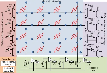
B. Architecture
The NanoPPUF, as shown in Fig. 3 consists of five major parts: (i) a memristor-based crossbar, (ii) a challenge and characterization circuit, (iii) a refresh and characterization circuit, (iv) a response circuit, and (v) a controller circuit. This architecture works in three phases which are described below.
a) Characterization phase
This is a one-time operation. In this phase, the individual devices are characterized to build an accurate SPICE model for the NanoPPUF. Characterization of a device involves determining its length, width, and thickness. Specifically for devices in [2], this process would follow these steps:
(i) Determine the HRS value: Switch off the device by applying a negative pulse of long duration (>50 ms for the device in [2]). Next, apply a positive pulse of magnitude Vdd of smaller duration. Measure the current (Iload) flowing
through the load resistor (Rload). The value of HRS is given
as:
- . (4) (ii) Determine the LRS value: switch on the device by applying a positive pulse of long duration (>50 ms for the device in [2]). Next, apply a negative pulse of magnitude Vdd and of smaller duration. Finally, measure the current
flowing through the load. The value of LRS is given as:
|
|- . (5) (iii) Determine the time to switch on (tON): Switch off
the device by applying a negative pulse of long duration (>50 ms for the device in [2]). Next, apply a positive pulse of smaller duration until the device switches on. The time to switch on (tON) is the duration of this positive pulse.
After measuring HRS, LRS, and ton values, one can solve
the following equations to obtain the values of L, W, and D:
,
,
- -
, (6) The above steps must be repeated for every memristor in the crossbar. At the end of this phase, the SPICE model for the NanoPPUF is developed.
b)Refresh phase
In this phase, all of the memristors are refreshed to a known state before the start of the protocol. All the memristors are switched to their HRS by applying a negative voltage pulse across them of sufficient duration. Thus, the changes in the memristance values of the memristors caused by previously applied challenges are erased. This phase uses the challenge and characterization circuit as well as the refresh and characterization circuit.
c) Challenge-response phase
In this phase, the challenge is applied by the challenge and characterization circuit and the response is measured by the response circuit. The controller circuit compensates for voltage and temperature fluctuations.
d)Measurement phase
In this phase, the voltages at the boundaries of the polyomino nodes selected by the verifier (Alice) will be measured using voltage sensors.
The different components of the NanoPPUF architecture are explained below.
1) Memristor-crossbar
A crossbar consists of N×N nanowires running perpendicular to each other with memristors at the intersections. The NanoPPUF also consists of tap points (shown as blue colored dots in Fig. 3) to measure the boundary conditions. These tap points are connected to voltage sensors to measure the voltages. On selecting a set of tap points, one can realize the polyomino in a crossbar. The selected tap points define the boundaries of a polyomino.
2) Challenge and characterization circuit
Challenges are applied to the left side of the memristor crossbar through the 2:1 multiplexer. Each challenge bit corresponds to one row. When a challenge bit is ‘1’, the multiplexer applies a voltage of magnitude Vdd to that
particular row. If the challenge bit is ‘0’ then that row is floated so that no current from the crossbar leaks through the rows. The floating rows do not eliminate sneak paths within a circuit but instead forces all of the sneak path currents to drain through the response circuit connected to the columns of the crossbar.
When the challenge bit is ‘1’, a positive pulse is applied to that corresponding row. While the amplitude of this pulse is Vdd, one can apply it for different durations. The
pulse is long enough to cause all of the memristors in the row to switch to the LRS. During the refresh phase, the left hand side of each row is made to float. During characterization, a positive pulse is applied only to the row in which the selected device resides. All other rows remain floating. C1 C2 R lo ad C Ire f R lo ad C Ire f R3
Iref & S/H controller R lo ad C Ire f R lo ad C Ire f C1 C2 Vdd Vdd Vdd Vdd -Vdd -Vdd -Vdd -Vdd Refresh 1 Refresh 2 Refresh 3 Refresh 4 C ha lle ng e & c ha ra ct er iz at io n ci rc ui t R efr es h & c ha ra cte riz ati on c irc uit Controller ckt Response circuit Volt. & Temp.
sensor S/H R4 S/H R2 S/H R1 S/H C/R C/R C/R C/R Memristor Crossbar
3) Refresh and characterization circuit
Similar to the challenge and characterization circuit, the refresh and characterization circuit also has two 2:1 multiplexers per row.
During the refresh phase, the multiplexers apply –Vdd to
the row. This pulse is long enough such that all of the memristors are switched to the HRS.
During the characterization phase, the multiplexers make the right hand side of the crossbar to float so that the characterization pulse passes only through the target device.
During the challenge-response phase, the multiplexers make the right hand of side of the crossbar to float so that sneak path currents drain only through the response circuit. 4) Response circuit
Each column of the crossbar generates a response bit. In the response circuit, each column of the crossbar consists of a load resistance (Rload), a current comparator, and a
sample and hold (S/H) circuit. The comparator compares the current flowing out the column (Iout) with that of the
reference current (Iref). If Iout is greater than Iref, then the
response bit is logic ‘1’, otherwise it is ‘0’. The S/H circuit latches the value of the output bit at the sample time, which is controlled by the controller circuit. The controller circuit also supplies Iref.
5) Controller circuit
The controller circuit has a look-up-table that stores pre-defined Iref and sample time values for different voltage
and temperature values. The purpose of the controller circuit is to sense the current supply voltage and temperature, and set the Iref and sample time values. This
circuit is similar to the one used in [31, 42].
C. Security Analysis 1) Simulation Setup
Simulation models of the memristor device fabricated in
[2] were developed based on the Team Model proposed in [42]. The parameters of this device are given in Table 1. To analyze the effect of variation, the thickness of the devices is varied within ±2%. To evaluate the security and stability metrics, we performed Monte Carlo simulations for 100 memristor-based crossbars using the HSPICE simulation tool [43]. For each crossbar we applied 100 challenges.
2) Size of the crossbar (N) vs Simulation Time
The size of the crossbar should be large enough such that it is computationally infeasible for an attacker to simulate the NanoPPUF but small enough to be fit into a chip. Therefore, one needs to determine the size of the crossbar that satisfies these two constraints. Fig. 4 shows the simulation time for different crossbar sizes and for different resistive devices. It can be seen that the memristor device with non-linear characteristics has a higher simulation time than the other devices. Thus, memristors with non-linear characteristics are attractive to build NanoPPUFs.
One can estimate the simulation time of a NanoPPUF by determining the polynomial equation that fits the data points shown in Fig. 4. Such polynomial equations can be estimated by using the curve fitting tool box in Matlab. On curve fitting the data values in Fig. 4, the simulation time of an N×N NanoPPUF is given as:
0.0175N3 + 0.412N2 + 4.99N + 2.39 s (7). From this equation, one can determine that in order to have a simulation time of 1000 days, the PPUF should be of size 1782×1782.
Furthermore, one can also derive the lower bound value of simulation time in the following way. Many SPICE simulation tools perform transient simulations of a circuit by multiplying its voltage and conductance matrices. The size of these matrices is equivalent to the number of nodes. In the case of the NanoPPUF with N×N memristors, these matrices are at least of the size N×N. As the complexity of matrix multiplication of size N×N is 2.373 N2 [44], the lower bound of simulation time for the NanoPPUF is also 2.373 N2.
3) Polyomino size (M) vs Simulation time
Increasing the polyomino size exponentially increases the number of possible polyominoes but also increases the
Fig. 4. Simulation time of different crossbar sizes for different resistive devices.
Table 1 Device parameters Parameter Value LRS 121KΩ HRS 121MΩ
L 50nm
D 50nm
W 50nm
μ 1e-9m2/(V·s)
p 0.5
α -40*1e-6
simulation time for Alice. Fig. 5 shows the number of possible polyominoes and the simulation times for different sizes of polyominoes. The left-side Y-axis is log scaled while the right-side Y-axis is linearly scaled. One can infer from the figure that even for a small size of the polyomino such as 20, the number of possible polyominoes is more than a billion. Mallory does not know which of these billion polyominoes that Alice will select for her simulation. With a polyomino size of 20, the simulation time for Alice is around 25 s which is feasible to perform real time authentication.
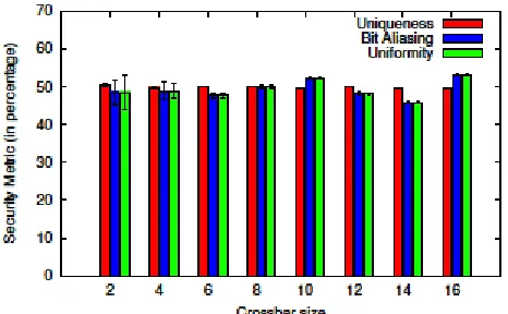
4) Unique responses
To analyze the NanoPPUF for producing unique IDs, we used three different metrics proposed by Maiti et al [45]. i) Uniqueness: The Hamming distance between the responses from two different crossbars upon application of the same challenge. The ideal value should be 50%. For k PPUFs, this metric is calculated as:
( - )∑ - ∑ ( ) , (8) where Ri and Rj are responses for the same challenge
applied to two different crossbars I and j. HD(Ri, Rj) is the
Hamming distance between the two responses.
ii) Uniformity: The proportion of 1’s and 0’s should be equal in a response to ensure the randomness of the response. The ideal value should be 50%. For an n-bit response i, this metric is calculated as:
∑ , (9)
where ri,l is ‘1’ if the lth bit of the response i is 1.
iii) Bit-aliasing: Because of bit-aliasing, different PPUFs may produce similar response bits. Consequently, the responses of these PPUFs will be more predictable. Hence, the response bits should not show any affinity towards either 0 or 1. Ideally, the value for bit-aliasing should be 50%. This metric is calculated by:
- ∑ . (10)
Fig. 6 shows the distribution of uniqueness, uniformity, and bit-aliasing results for different crossbar sizes. It also shows a 95% confidence interval via the error bars. One can see that results are close to the ideal value of 50%. Furthermore, the spread of the confidence intervals is at most 3%. These results indicate that the responses of the PPUF are highly unique, making NanoPPUFs excellent candidates for unique identification.
5) Stability against voltage fluctuations
The response of the NanoPPUF has to be stable irrespective of environmental variations. To estimate the reliability of the NanoPPUF against voltage fluctuations, we first apply a challenge and calculate the NanoPPUF’s response at nominal operating conditions (1 V for 32 nm CMOS technology). We then obtain the response for the same challenge at different voltage conditions.. We estimate the reliability of NanoPPUF using two different metrics: correctness and reliability.
i) Correctness: For voltage fluctuations, correctness is the maximum closeness between the responses at nominal voltage
and under different operating voltages in terms of Hamming distance. Ideally, this value should be 100%. For an N-bit response, this value is calculated as:
- ∑ ( )
, (11)
where Rv is the response for challenge C at different
operating voltages (different from nominal voltage) and
Rnominal is the response for challenge C at nominal voltage.
ii) Reliability: This metric is similar to that of correctness, differing only by a factor. Again for voltage fluctuations, reliability is the average closeness between the responses at nominal voltage and at different operating voltages in terms of Hamming distance. Ideally, this value should be 100%. For an N-bit response, this value is calculated as:
- ∑ ( )
, (12)
where Rv is the response for challenge C at different
operating voltages (different from nominal voltage) and
Rnominal is the response for challenge C at nominal voltage.
Fig. 7 shows the correctness and reliability results for voltage fluctuations for an 8×8 crossbar. Even though the correctness and reliability values decrease at higher voltages, the minimum value is still greater than 90%. Furthermore, the spread of the 95% confidence interval is at most ±1%. Thus, the NanoPPUF produces reliable responses even in the presence of voltage fluctuations.
Fig. 6. Uniqueness, Bit aliasing, and Uniformity of NanoPPUF for different sizes of crossbar
D. Protocols
We will outline some important two-party security protocols enabled by a NanoPPUF. Alice’s and Bob’s NanoPPUFs are denoted as PPUFA and PPUFB, respectively. The challenge C is the input and the response R is the corresponding output of the NanoPPUF. B represents the set of boundary conditions (voltage values) of a selected polyomino in a NanoPPUF crossbar. The challenge set X is the list of pins where the challenge vector C is applied. The length of C and the length of the challenges in X are equal.
1) User Authentication
NanoPPUF-based authentication can prevent adversarial spoofing and identity theft. We propose a user authentication protocol. It uses a NanoPPUF which is large enough that it is computationally infeasible to simulate it even for a single challenge
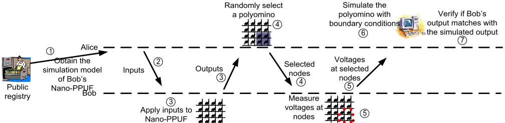
Protocol 1: Assume that Alice wishes to authenticate that she is indeed conversing with Bob and not a malicious adversary pretending to be Bob. Alice issues a challenge C to Bob. Bob applies the challenge to his physical NanoPPUF, PPUFB, and returns the response R to Alice. Given this challenge-response pair, Alice can validate the authenticity of Bob. Fig. 8 shows a time-bounded authentication protocol using a NanoPPUF. Due to the exponentially large number of polyominoes in the NanoPPUF and the bi-directionality of the NanoPPUF, Alice can simulate selected polyominoes and validate the inputs and outputs along the boundaries of the selected polyomino using node voltage analysis.
An adversary, Mallory, masquerading as Bob has to respond to Alice with a full output response R. Alice can safely pick a random polyomino from among the exponential number of polyominoes in this large NanoPPUF grid to validate the challenge and response on PPUFB. The adversary has near-zero probability of randomly guessing the chosen polyomino. For additional security, Alice could use two or more polyominoes or even request responses from Bob to two or more challenges. 2) Remote Secret Key Exchange
Remote Secret Key Exchange, also known as public key communication, allows Alice and Bob to securely
communicate by encrypting their messages with a secret key. A challenge to the NanoPPUF can be used as the secret key. For this protocol, the size of the NanoPPUF is substantially reduced so that one can simulate it in real time.
When Alice decides to send a message to Bob, she simulates a secret key CB on PPUFB and calculates . Bob receives a copy of RB, the encrypted message,
, and the input challenge set X on which the challenge was applied. Since Bob owns the NanoPPUF that originally output , he determines the secret key to decrypt the message by iterating through all the challenges in X on the given input set until the challenge C is found such that . For these reasons an eavesdropper is unlikely to find the secret key via simulation.
E. Advantages over CMOS-based PPUFs
SIMulation Possible but Laborious (SIMPL) systems were proposed for time-bounded authentication [39]. SIMPL systems were constructed using Cellular Non-linear Networks and SRAM cells [39]. However, the time difference between the execution of an input on a SIMPL token and simulation of a SIMPL model has not been proven. This may preclude their use in two-party protocols
Alice
Bob
Inputs
Apply inputs to Nano-PPUF
Outputs
Randomly select a polyomino
Selected nodes
Measure voltages at
nodes
Voltages at selected
nodes Simulate the polyomino with boundary conditions
Verify if Bob’s output matches with the simulated output
Obtain the simulation model
of Bob’s Nano-PPUF Public
registry
1
2
3
3
4
4
5 5
6
7
Fig. 8. Protocol for time-bounded authentication using NanoPPUF.
Protocol 2. Remote Secret Key Exchange 1: Alice simulates secret challenge on PPUFB,
recording response ( is the secret key). 2: Alice chooses message m, computes . 3: Alice sends and challenge set X to Bob. 4: Bob iterates through challenges on X until RB is
found.
5: Bob computes m = M B.
Protocol 1. Authentication 1: Alice sends challenge C to Bob.
2: Bob applies challenge C to PPUFB and records response R.
3: Bob sends R to Alice.
4: Alice picks a random polyomino P of PPUFB and sends it to Bob.
5: Bob measures the boundary voltages of P and sends them to Alice.
6: Alice simulates the boundary conditions (C and R) on P to check that node voltage analysis converges correctly.
like bit commitment, oblivious transfer, zero-knowledge proofs, and coin flipping that requires an exponential difference [48].
Another CMOS-based PPUF uses XOR networks [38]. This PPUF also assumes that the simulation of the entire PPUF circuit is computationally impossible. However, their simulation model is simpler than that for nanoelectronic devices for a variety of reasons including their unidirectional nature. Hence, to achieve a desired security level (simulation time), the CMOS-based PPUF has to be substantially larger. Such large CMOS-based PPUFs have a very large latency which precludes their usage in real-time systems.
Nano-PPUF solves these problems as they have a very high simulation time compared to SIMPL and CMOS-based PPUFs due to the inherent bidirectionality of memristors. Furthermore, the size and speed of the memristors ensure that NanoPPUF is more compact and can operate at higher speeds than SIMPL and CMOS-based PPUFs.
F. Challenges
It is essential to consider several challenges in designing a NanoPPUF. Failure to do so could jeopardize the integrity of the system by wrongly authenticating a fraudulent user or disavowing a legitimate user.
Modeling errors: NanoPPUFs require accurate modeling of all device and circuit parameters, including the resistances and parasitic capacitances in the crossbar. However, achieving a high degree of modeling accuracy is a significant challenge. Thus, there will likely be tradeoffs between the size of the crossbar and the achievable degree of model fidelity.
Impact of peripherals (sense amplifiers and row/column drivers): The sense amplifiers used to measure the output voltage in the crossbar have an inherent noise margin. This noise margin can lead to ambiguous results, thereby resulting in uncharacteristic outputs.
Impact of temperature and voltage fluctuations on stability: The behavior of nanoelectronic devices typically vary with temperature. Thus, the outputs of crossbars built with these nanoelectronic devices will also vary with temperature and result in uncharacteristic outputs. Device physicists have demonstrated significant progress in fabricating nanoelectronic devices that are stable over a range of temperatures. For instance, [26] has demonstrated a memristor that exhibits a stable operation over temperatures from 0-150˚C.
Reduced order simulation of crossbars/cubes and its impact on security: The security of the NanoPPUF strongly depends on the complexity of the device model. If one can build a reduced of model of the device, e.g. a piece-wise linear model, and still can accurately predict both the device and crossbar behaviors, the security of the system will be reduced as the attacker is now required to spend only a little computational effort.
IV. NANOELECTRONICS SECURITY TOKENS A. Memristor-based Random Number Generator
Random number generators are important security primitives as they are used in generating session keys which are essential to establish secure communication channels.
Certain memristors can be used to generate random numbers as shown in Fig. 9 [4]. In these devices, trapped electrons in the insulation layer will randomly impact the current flowing through the filament channel. Upon
applying a high voltage (3 V for the memristor device in [4]), the current flowing through the filament will be too large to be impacted by the trapped electrons. However, on applying a low voltage (1.2 V), the width of the filament shrinks down; and the current flowing through the filament is strongly influenced by the trapped electrons. Since the number of trapped electrons is random, the output current will also be random. This method has great promise since it successfully passes several randomness tests designed by the National Institute of Science and Technology (NIST). B. Memristor-based Unique Signatures (MUS)
Certain memristors can be used to generate a unique signature for hardware [23] by exploiting two different characteristics of memristors: 1) inherent, non-uniform, irreproducible process variations during fabrication and 2) “forming” requirement to make them functional. [23] uses a pair of nonpolar memristors in series as a random bit generator, where the bit generation is a function of the location of a low resistance filament. Multiple instances of such random bit generators can produce a random word. Since this signature is non-volatile, it may be used for hardware identification purposes. This kind of embedded hardware ID can be used to thwart electronic counterfeiting or detect refurbished components.
1) Architecture
Consider a pair of memristors in series as shown in Fig. 10. The bottom metal electrode (BE) and the insulator layer are common for the two devices. Each memristor has its own top metal electrode (TE).
Conductive filament path
Insulator
Bottom electrode Top electrode
External current
2) Protocol
During the forming step, one TE is biased while the other TE is grounded. Two low resistance filaments are formed, one beneath each TE, through the insulator material layer. During the RESET operation, the resistance values of the two series memristors are returned to the HRS. During this switch, only one of the low resistance filaments becomes highly resistive; the other filament remains of low resistivity. The location of this latter filament serves as the random bit value. This location depends on the process-induced variations in insulator layer thickness and dopant concentration. The low resistance filament location is also impervious to additional SET and RESET operations. Thus, a unique signature is generated for the hardware. This signature will not be determined prior to the “formation” step. Thus, an attacker in the manufacturing unit could not read this unique signature and spoof it.
C. Advantages over CMOS-based Random Number Generators
In CMOS technology, the inherent process-induced variations in the FPGAs are leveraged to generate random numbers [24], where circuits such as ring oscillators are
used for randomness extraction.
However, the extracted random values are unstable since the frequency of a ring oscillator is strongly temperature dependent.
A unique device signature in CMOS can also be derived from an unwritten Static Random Access Memory (SRAM) circuit. An SRAM cell consists of two transistors connected in a butterfly-like fashion. Due to threshold voltage mismatch caused by process variations, one transistor will be stronger than the other. This mismatch is then used to generate the random signature. However, an attacker in the manufacturing unit can easily read-out this unique signature and use it to spoof the hardware. Unlike with the MUS, this tampering is not irrefutable.
Similar to generating random signatures using memristor-based crossbars, diode-based crossbars are also used to generate random signatures [25]. The randomness arises from the variation in the amount of dopants in the diodes. Unfortunately, an attacker may still read-out the signature from the diodes since they do not require a forming process.
Nanoelectronic devices whose operations are inherently invariant with temperature can be used to generate random numbers. Recently, Contact Resistive Random Access Memory (CRRAM), whose characteristics are stable over
a range of temperatures (0-150 ˚C), was used to generate random numbers [4,26].
V. NANOELECTRONICS-BASED TAMPER DETECTION AND FORENSICS
Memristors can be used for tamper detection and digital forensic analysis. Tamper detection entails identifying unauthorized usage of or access to the target hardware. Digital forensics entails recovering data from the hardware. We will show how the device formation, non-volatility, and memristance drift can be leveraged for tamper detection and forensics.
A. Manufacture-time Tamper Detection for Trust Verification
The memristive device formation step enables one to differentiate a virgin (i.e. unformed) device from one that has been used (i.e. formed). Consider a system where a memristor or group of memristors is required for a particular circuit to function. For example, a group of memristors could be part of a circuit used to encrypt data in a secure microprocessor. Any user (authorized or unauthorized) would need to form these devices before gleaning any useful information. A “trust but verify” technique can be used to obtain some information as to whether or not a circuit has been tampered with. Such a technique is useful to verify the trustworthiness of the new integrated circuits received from an untrustworthy fabrication facility. The technique would work by first writing a known value to the memristor(s), reading that value back, writing the complement of the known value to the memristor(s), reading the next value back, and comparing the results. If the formation step had not occurred, then it would not be possible to write to the memristor(s) and the result of the comparison would show the values read were the same. However, if the memristors have been formed, then the comparison will show that the values read will be different. This second case could be an evidence of possible tampering of the circuit.
B. Run-time Tamper Detection in Memristor-based Memories
1) Memristor-based crossbar memories
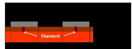
An N×N memristor crossbar consists of two sets of N wires running orthogonal to each other, where a memristor is grown at the cross points as shown in Fig. 1 (c). There are two kinds of paths in the crossbar: direct path and sneak path. In a direct path, current flowing from an input (row) to an output (column) is the function of the resistance of the device at the cross point of that input and output. In a sneak path, the current flowing from an input to an output is a function of the resistance of devices at other cross points in the crossbar. Such memristor-based crossbars have been used to build non-volatile memories. In these memories, the HRS and LRS are used to represent logic ‘0’ and ‘1’, respectively [19,20].
Write operation: To write into a particular device, VRESET
(for logic 0) or VSET (for logic 1) is applied to the
corresponding row and 0 V is applied to the corresponding column.
Read operation: To read a particular device, a read voltage, usually a positive pulse of small amplitude, is applied to the corresponding row. The current flowing out of the corresponding column is compared with a reference current. If the output current is greater than the reference current, then a ‘1’ is read, otherwise a ‘0’ is read. In devices where the memristance drifts, applying a read voltage across the memristor can cause its memristance to drift. Hence, in order to undo this change caused by memristance drift during the read operation, a two-stage read operation is used [21]. For a bipolar memristor, the ideal read pattern uses a positive pulse immediately followed by a negative pulse of the same magnitude and duration, creating a zero net change in memristance. 2) Tamper detection
Unauthorized memory reads in memristor-based memories can be detected as follows [19]. Consider the memristor-based crossbar memory shown in Fig. 1(c). In this memory, the HRS and LRS are used to represent logic ‘0’ and ‘1’, respectively. The key idea to detect an unauthorized read operation is to monitor the associated drift in memristance.
In order to cover his trail, the attacker (after performing the unauthorized read) may restore the memristance of the device to its original value by unreading (e.g. by applying a read pulse of opposite polarity but with the same magnitude and for the same duration) the device. The memristance then drifts in the opposite direction by the same amount and returns to the original value.
To prevent the attacker from restoring the memristance value, the memory read operation is modified as shown in Fig. 2 [19]. The modified memory read operation uses two consecutive read pulses. While the magnitude and duration of the first pulse are public (i.e. known to the attacker as well), the magnitude and duration of the second pulse are private and known only to the authorized user. Thus, even though an attacker can restore the memristance value to its initial value using a pulse of opposite polarity, he cannot revert back the change in resistance caused by the second pulse with its private parameters. This way, the memristance value following an unauthorized read
operation will be different from the initial memristance value before the read and cannot be undone. The authorized user can detect this change in memristance and consequently the tampering.
C. Forensics in Memristor-based Threshold Logic
Memristor-based digital logic gates have been proposed in prior work [22]. We show that such gates can be useful from a forensics perspective.
1) Preliminaries: Memristor-based threshold gates Consider the memristor-based threshold logic (MTL) gates proposed in [22]. In an MTL gate, the memristors are used as weights on the inputs of the gate. Fig. 3(a) shows a 3-input threshold gate which uses three memristors MA, MB, and MC to weigh the current flowing from the inputs A, B, and C, respectively. The current mirrors isolate the currents flowing through the different inputs. The current comparator is then used to compare the sum of the weighted currents against the reference current Iref. If the
summed current is greater than Iref, then the output is logic
‘1’, else the output is logic ‘0’. A positive voltage denotes logic ‘1’, and a 0 V denotes logic ‘0’.
2) Effect of memristance drift on MTL gates
As discussed previously, when logic ‘1’ (positive voltage) is applied to an input, the memristance value of the corresponding memristor drifts. On the other hand, there will not be any drift when logic ‘0’ is applied. The amount of drift depends on the number of logic ‘1’s applied to that input. For example, consider an MTL gate implementing an AND function. The memristance values of the memristors are 2 MΩ. Let the amplitude and duration of input pulses be 1.1 V and 2 ns, respectively. Consider one million, two million and three million 1’s are applied to inputs A, B, and C, respectively. Now the final memristance values of memristors MA, MB, and MC will be
2.12 MΩ, 2.25 MΩ, and 2.38 MΩ, respectively. These changes in memristance values are caused by memristance drift.
3) Forensic analysis
Conversely, if one determines that the final memristance values of memristors MA, MB, and MC are
2.12 MΩ, 2.25 MΩ, and 2.38 MΩ, respectively, then forensic analysis can estimate that about one million, two million, and three million 1’s have been applied to the inputs A, B, and C, respectively.
Consider extending this forensic analysis from individual gates to circuits. The number of 1’s received by
x
0x
1x
21 2
Fig. 11. The dark and lightly shaded regions represent the high-resistive and low-resistive regions, respectively. The dotted line represnts the location of the domain wall which determines the current resistant value. Every read operation uses two pulses. The magnitude and duration of the first pulse are public, whereas the magnitude and duration of the second pulse are known only to the defender.
Iref
A
B
C MA
MB
MC
F
F
Isolator Current mirror
Current comparator
O2 O1 I1
I2 I3 I4 I5
G1
G2 G3
G4 G5
G6
(a) (b)
an input of a gate depends on its location within the circuit. Consequently, the memristance change at the inputs of different gates will be different. Consider the C17 circuit, one of the ISCAS’85 benchmark circuits, shown in Fig. 3(b). Let us name the memristors based on the signals/gates that feed them. On applying the input pattern ‘11111’, the memristance values of the memristors I1–I5 and G3–G5 will change. Similarly, on applying the input pattern ‘00000’, the memristance values of the memristors G1–G4 will change. Note that the memristance values of the memristors G3 and G4 change for both patterns.
By measuring the change in the memristance of a memristor, one can determine the number of ’1’s received at that input. Similarly, the number of ‘1’s received by all the memristors in the circuit can be determined.
After measuring the changes in memristance values, a forensic analyst can make the following observations. If none of the memristors had drifted, then the hardware was never used. If a set of memristors had drifted, then he can identify a set of input patterns that may have been applied to the hardware which caused that drift. For instance, if only the memristors I1–I5 and G3–G5 had drifted, then he will identify the input pattern applied to the hardware as ‘11111’. If the memristor G3 had drifted more than the other gates, then he infers that input patterns applied are ‘d0ddd’, ‘d100d’, ‘d101d’, and/or ‘d110d’2, where d represents a “don’t care” bit value.
D. Advantages over Forensics in CMOS-based Designs Forensic analysis of CMOS-based designs has not been explored to the best knowledge of the authors. However, similar to memristance drift for memristors, one can leverage the Negative Bias Temperature Instability (NBTI) effect in CMOS for forensics. NBTI occurs in a CMOS transistor when electron traps are formed at the silicon-silicon dioxide interface. The NBTI effect in PMOS is more dominant than it is in NMOS. Applying logic ‘1’ to the PMOS transistor subjects it to NBTI stress which then degrades the threshold voltage of the transistor and thereby increases its delay. A forensic analysis can detect this change if one can determine the number of logic 1’s received by that transistor. Unfortunately, the rate of change in transistor delay due to NBTI is slow (on the order of a few years) when compared to the instantaneous change in memristance values due to memristance drift. E. Outstanding Challenges
To perform tamper detection in memristors and memristor-based memories and forensic analysis in MTL gates, changes in memristance values have to be accurately sensed. This requires designing highly sensitive sense amplifiers. Such sense amplifiers are typically large and consume more power. In the case of tamper detection in memristor-based memories, the amplitude and duration of the second pulse has to be adjusted so that the read and write margins of the devices are honored. Similarly, in the case of forensic analysis on MTL gates, increasing either
the duration or amplitude of the input pulses will significantly change the memristance value of the device, thereby making forensic analysis easier. However, changes in memristance values over time also move the weights of MTL gates out of range, making the hardware non-functional. An authorized user has to once again restore the memristors to their initial memristance values. While decreasing the duration or amplitude of the input pulses will increase the usage time of the hardware, it makes the forensic analysis harder as the change in memristance values will be small. Thus, the duration and amplitude of input pulses have to be optimized for hardware usage time and ease of forensic analysis.
VI. CONCLUSIONS
We highlighted the important characteristics of memristors and demonstrated how they can be used to build new security primitives. These characteristics are based on experimental and theoretical device research. Characteristics of other nanoelectronic devices such as spintronics, phase change materials, graphene, and quantum dots remain to be explored for their applications in security. Another important direction is for device physicists to engineer nanoelectronic devices not only for memory and logic applications but also for security applications. Security researchers should develop new security primitives, protocols, and associated mathematical proofs by abstracting the detailed characteristics of nanoelectronic devices. Circuit designers are the bridge between device engineers and security researchers, harnessing these devices characteristics to satisfy security requirements.
REFERENCES
[1] L. Chua, “Memristor-the missing circuit element,” IEEE Transactions on Circuit Theory, vol. 18, no. 5, pp. 507 – 519, 1971.
[2] D. B. Strukov, G. S. Snider, D. R. Stewart and R. S. Williams “How we found the Missing Memristor,” Nature, vol. 453, pp. 80–83, 2008.
[3] Y.T. Chiu, “A Memristor True Random-Number Generator”, IEEE Spectrum, 2012.
[4] C.Y. Huang, W.C. Shen, Y.H Tseng, Y.C. King, and C.J. Lin, "A Contact-Resistive Random-Access-Memory-Based True Random Number Generator," IEEE Electron Device Letters, vol.33, no.8, pp.1108-1110, 2012
[5] N.R. McDonald, S.M. Bishop, B.D. Briggs, J.E. Van Nostrand, and N.C. Cady, “Influence of the plasma oxidation power on the switching properties of Al/CuxO/Cu memristive devices”, Solid-State Electronics, Vol. 78, pp. 46-50 (2012)
[6] Oblea, A.S.; Timilsina, A.; Moore, D.; Campbell, K.A., "Silver chalcogenide based memristor devices," International Joint Conference on Neural Networks (IJCNN), pp.1-3, 2010
[7] R. Waser and M. Aono, “Nanoionics-based resistive switching memories,” Nature Materials, Vol. 6, pp. 833–840, 2007.
[8] L. Goux, J. G. Lisoni, M. Jurczak, D. J. Wouters, L. Courtade, and Ch. Muller, “Coexistence of the bipolar and unipolar resistive-switching modes in NiO cells made by thermal oxidation of Ni layers,” Journal of Applied Physics, vol. 107, no. 2, pp. 024512 - 024512-7, 2010.
[9] B.D. Briggs, S.M. Bishop, K.D. Leedy, B. Butcher, R. L. Moore, S. W. Novak and N.C. Cady, “Influence of Copper on the Switching Properties of Hafnium Oxide-Based Resistive Memory,” MRS Proceedings, vol. 1337, 2011
layers,” Applied Physics Letters, vol. 88, no. 23 pp. 232112 - 232112-3, 2006.
[11] K. Szot, W. Speier, G. Bihlmayer, and R. Waser, “Switching the electrical resistance of individual dislocations in single crystalline SrTiO3,” Nature Materials, vol. 5, pp. 312–320, 2006
[12] J. C. Scott and L. D. Bozano, “Nonvolatile memory elements based on organic materials,” Advanced Materials, vol. 19, pp. 1452– 1463, 2007.
[13] N. B. Zhitenev, A. Sidorenko, D. M. Tennant, and R. A. Cirelli, “Chemical modification of the electronic conducting states in polymer nanodevices,” Nature Nanotechonlogy, vol. 2, pp. 237–242, 2007.
[14] Y. N. Joglekar and S. J. Wolf, “The elusive memristor: properties of basic electrical circuits,” European Journal of Physics, vol. 30, no. 4, pp. 661–675, 2009
[15] Q. Xia, et. al. “Memristor−CMOS Hybrid Integrated Circuits for Reconfigurable Logic”, Nano Letters, vol. 9, no. 10, 2009
[16] J. Rajendran, H. Manem, R. Karri and G.S. Rose, “Approach to Tolerate Process Related Variations inMemristor-Based Applications,” Intl Conf. on VLSI Design, pp. 18–23, 2011.
[17] D. Niu, Y. Chen, C. Xu, Y. Xie, "Impact of process variations on emerging memristor," in the Proceedings of IEEE/ACM Design Automation Conference, pp. 877-882, 2010
[18] S. Kwon, S. Kang, K. Kim, "Controlling the temperature coefficient of resistance and resistivity in RuO2–TiO2 thin films by the intermixing ratios between RuO2 and TiO2," Applied Physics Letters, vol.92, no.18, pp.181903,181903-3, May 2008
[19] Xiaobin Wang; Yiran Chen;, "Spintronic memristor devices and application," in the Proc. of the IEEE Intl. Conf. on Design, Automation and Test in Europe, pp. 667-672, 2010.
[20] H. Manem, J. Rajendran, G. S. Rose, “Design Considerations for Multilevel CMOS/Nano Memristive Memory”, ACM Journal of Emerging Technologies in Computing, vol. 8, no. 1, pp. 1-22, 2012.
[21] Y. Ho, G. M. Huang, and P. Li, "Nonvolatile memristor memory: device characteristics and design implications," in the Proc. of IEEE/ACM Intl. Conf. on Computer-Aided Design, pp. 485 - 490, 2009
[22] J. Rajendran, H. Manem, R. Karri, G. S. Rose, “An Energy-Efficient Memristive Threshold Logic Circuit”, IEEE Transactions on Computers, vol. 61, no. 4, pp. 474-487, 2012.
[23] N.R. McDonald, “Al/CuxO/Cu Memristive Devices: Fabrication, Characterization, and Modeling,” M.S., College of Nanoscale Science and Engineering, University at Albany, SUNY, Albany, NY, 2012, 1517153
[24] P. Kohlbrenner and K. Gaj. “An embedded true random number generator for FPGAs”, in the Proc. of the ACM Intl. Conf. Field programmable gate array, pp. 71-78, 2004.
[25] U. R hrmair, C. Jaeger, M. Bator, M. Stutzmann, P. Lugli, and G. Csaba, "Applications of High-Capacity Crossbar Memories in Cryptography," IEEE Transactions on Nanotechnology, vol.10, no.3, pp.489-498, 2011.
[26] Y. H. Tseng, W. C. Shen, and C. J. Lin, “Modeling of electron conduction in contact RRAM (CR-RAM) devices as random telegraph noise,” Journal of Applied Physics, vol. 111, no. 7, pp. 073701 - 073701-5, 2012.
[27] B. Gassend, D. Clarke, M. van Dijk, and S. Devadas, “Silicon physical random functions,” in the Proc. of the ACM Intl. Conf. on Computer and Communications Security, pp. 148–160, 2002.
[28] G. E. Suh and S. Devadas, "Physical unclonable functions for device authentication and secret key generation," in the Proceedings of IEEE/ACM Design Automation Conference, pp. 9-14, 2007.
[29] D. Lim, J. Lee, B. Gassend, G. Suh, M. van Dijk, and S. Devadas, "Extracting secret keys from integrated circuits," IEEE Transactions on Very Large Scale Integration Systems, vol.13, no.10. pp.1200-1205, 2005 [30] S. Kumar, J. Guajardo, R. Maes, G.-J. Schrijen, and P. Tuyls, "Extended abstract: The butterfly PUF protecting IP on every FPGA," in the Proceedings of IEEE Hardware-Oriented Security and Trust, pp. 67-70, 2008.
[31] R. Helinski, D. Acharyya, and J. Plusquellic, "A physical unclonable function defined using power distribution system equivalent resistance variations," in the Proceedings of IEEE/ACM Design Automation Conference, pp. 676-681, 2009.
[32] J. Guajardo, S. Kumar, G.-J. Schrijen, and P. Tuyls,“Physical unclonable functions and public-key crypto for FPGA IP protection,” in the Proc. of the IEEE Intl. Conf. on Field Programmable Logic and Applications, pp. 189–195, 2007.
[33] A. R. Krishna, S. Narasimhan, X. Wang, and X. Wang, "Mecca: a robust low-overhead PUF using embedded memory array," in the Proceedings of International Conference on Cryptographic hardware and embedded systems, pp. 407-420, 2011
[34] U. Ruhrmair, S. Devadas, and F. Koushanfar, "Security based on Physical Unclonability and Disorder," Springer, 2011.
[35] F. Armknecht, R. Maes, A. Sadeghi, F.-X. Standaert, and C. Wachsmann, “A formalization of the security features of physical functions,” in IEEE Symposium on Security and Privacy, pp. 397–412, 2011.
[36] R. Maes and I. Verbauwhede, “Physically Unclonable Functions: a Study on the State of the Art and Future Research Directions,” in Towards Hardware-Intrinsic Security, Springer, 2010.
[37] G. E. Suh, C. W. O’Donnell, I. Sachdev, and S. Devadas, “Design and implementation of the AEGIS single-chip secure processor using physical random functions,” in the Proc. of IEEE/ACM Intl. Conf. on Computer Architecture, pp. 25–36, May 2005.
[38] N. Beckmann and M. Potkonjak, "Hardware-Based Public-Key Cryptography with Public Physically Unclonable Functions", in the Proc. of Intl. Workshop on Information Hiding, pp. 206-220, 2009
[39] U. Rührmair, Q. Chen, P. Lugli, U. Schlichtmann, M. Stutzmann, and G. Csaba, “Towards Electrical, Integrated Implementations of SIMPL Systems”, Information Security Theory and Practices. Security and Privacy of Pervasive Systems and Smart Devices, Lecture Notes in Computer Science, vol. 6033, pp. 177-292, 2009.
[40] J. Rajendran, G. S. Rose, R. Karri, and M. Potkonjak, “Nano-PPUF: A Memristor-based Security Primitive”, in the Proc. of IEEE Intl. Conf. on VLSI, pp. 84-87, 2012.
[41] I. Jensen and A. J. Guttmann, “Statistics of lattice animals (polyominoes) and polygons,” Journal of Physics A: Mathematical and General, vol. 33, pp. L257–L263, 2000.
[42] S. Kvatinsky, E.G. Friedman, A. Kolodny, U.C. Weiser, "TEAM: ThrEshold Adaptive Memristor Model," IEEE Transactions on Circuits and Systems I, vol.60, no.1, pp.211,221, Jan. 2013
[43] Synopsys, "HSPICE" http://www.synopsys.com/tools/Verification/AMSVerification/CircuitSi mulation/HSPICE/Pages/default.aspx
[44] A. Stothers, "On the Complexity of Matrix Multiplication", [PhD Thesis], www.maths.ed.ac.uk/pg/thesis/stothers.pdf
[45] A. Maiti, I. Kim, P. Schaumont, "A Robust Physical Unclonable Function With Enhanced Challenge-Response Set," IEEE Transactions on Information Forensics and Security, vol.7, no.1, pp.333,345, Feb. 2012
[46] S. Haber and W. S. Stornetta, “How to time-stamp a digital document,” Journal of Cryptology, vol. 3, no. 2, pp. 99-111, 1991.
[47] M. Blum, “Coin flipping by telephone a protocol for solving impossible problems,” Proceedings of CRYPTO, pp. 11-15, 1981.
![Fig. 1. (a) Metal-insulator-metal (MIM) memristor structure [2], (b) Theoretical Current-voltage characteristics of a bipolar memristor [5], (c) A 3x3 memristor-based memory that can function as a memory](https://thumb-us.123doks.com/thumbv2/123dok_us/7885088.1308327/2.612.82.531.58.229/insulator-memristor-structure-theoretical-characteristics-memristor-memristor-function.webp)