Chapter 8
Why are Timer Functions Important?
• It is very difficult and impossible to implement the
following applications without a timer function:
– Time delay creation and measurement
– Period and pulse width measurement
– Frequency measurement
– Event counting
– Arrival time comparison
– Time-of-day tracking
The HCS12 Timer System
(1 of 2)
•
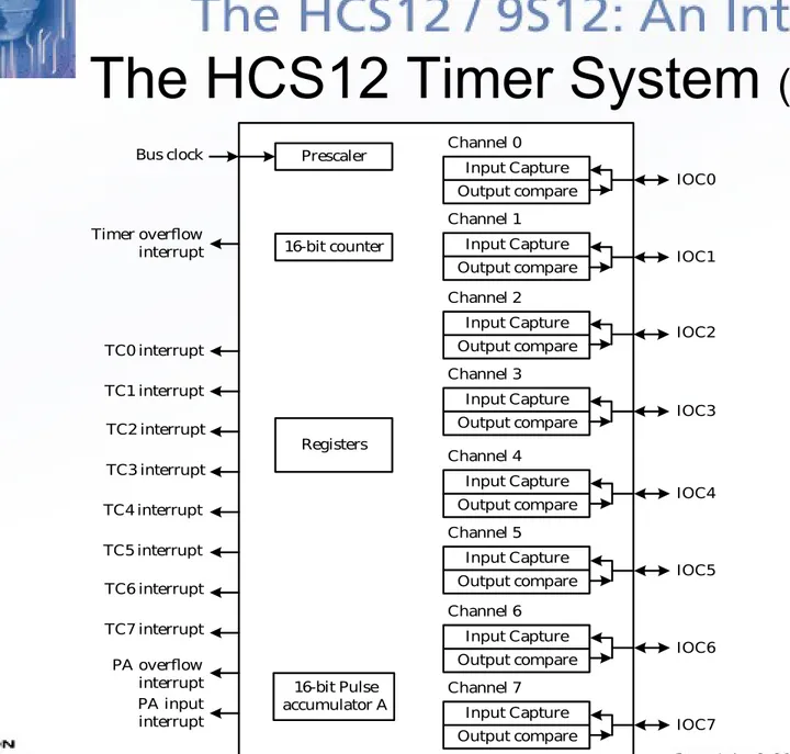
The HCS12 has a standard timer module (TIM) that consists of:
– Eight channels of multiplexed input capture and output compare functions. – 16-bit pulse accumulator A
– 16-bit timer counter
– The TIM block diagram is shown in Figure 8.1.
•
The HCS12 devices in the automotive family have implemented an
Enhanced Capture Timer module (ECT). The ECT module contains:
– All the features contained in the TIM module
– One 16-bit buffer register for each of the input capture channels – Four 8-bit pulse accumulator
– A 16-bit Modulus Down Counter with 4-bit prescaler
– Four user selectable delay counters for increasing input noise immunity
Prescaler 16-bit counter Input Capture Output compare Channel 0 Input Capture Output compare Channel 1 Input Capture Output compare Channel 2 Input Capture Output compare Channel 3 Input Capture Output compare Channel 4 Input Capture Output compare Channel 5 Input Capture Output compare Channel 6 Input Capture Output compare Channel 7 Registers 16-bit Pulse accumulator A IOC0 IOC1 IOC2 IOC3 IOC4 IOC5 IOC6 IOC7 Bus clock Timer overflow interrupt TC0 interrupt TC1 interrupt TC2 interrupt TC3 interrupt TC4 interrupt TC5 interrupt TC6 interrupt TC7 interrupt PA overflow interrupt PA input interrupt
Figure 8.1 HCS12 Standard Timer (TIM) block diagram
Timer Counter Register (TCNT)
• Required for input capture and output compare
functions
• Must be accessed in one 16-bit operation in
order to obtain the correct value
7 6 5 4 3 2 1 0
TEN TSWAI TSFRZ TFFCA 0 0 0 0
value
after reset 0 0 0 0 0 0 0 0
TEN -- timer enable bit
0 = disable timer; this can be used to save power consumption 1 = allows timer to function normally
TSWAI -- timer stops while in wait mode bit
0 = allows timer to continue running during wait mode 1 = disables timer when MCU is in wait mode
TSFRZ -- timer and modulus counter stop while in freeze mode
0 = allows timer and modulus counter to continue running while in freeze mode
1 = disables timer and modulus counter when MCU is in freeze mode TFFCA -- timer fast flag clear all bit
0 = allows timer flag clearing to function normally
1 = For TFLG1, a read from an input capture or a write to
the output compare channel causes the corresponding channel flag, CnF, to be cleared. For TFLG2, any access to the TCNT register clears the TOF flag. Any access to the PACN3 and
PACN2 registers clears the PAOVF and PAIF flags in the PAFLG register. Any access to the PACN1 and PACN0 registers clears the PBOVF flag in the PBFLG register.
Figure 8.2 Timer system control register 1 (TSCR1)
Timer System Control Register 1 (TSCR1)
• The contents of TSCR1 are
shown in Figure 8.2.
• Setting and clearing the bit 7
of TSCR1 will start and stop
the counting of the TCNT.
• Setting the bit 4 will enable
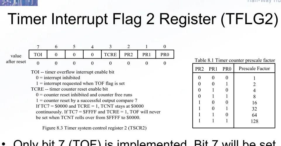
Timer System Control Register 2
(TSCR2)
• Bit 7 is the TCNT overflow interrupt enable bit.
• TCNT can be reset to 0 when TCNT equals TC7
by setting bit 3 of TSCR2.
• The clock input to TCNT can be prescaled by a
factor selecting by bits 2 to 0 of TSCR2.
7 6 5 4 3 2 1 0
TOI 0 0 0 TCRE PR2 PR1 PR0
value
after reset 0 0 0 0 0 0 0 0
TOI -- timer overflow interrupt enable bit 0 = interrupt inhibited
1 = interrupt requested when TOF flag is set TCRE -- timer counter reset enable bit
0 = counter reset inhibited and counter free runs 1 = counter reset by a successful output compare 7 If TC7 = $0000 and TCRE = 1, TCNT stays at $0000
continuously. If TC7 = $FFFF and TCRE = 1, TOF will never be set when TCNT rolls over from $FFFF to $0000.
Figure 8.3 Timer system control register 2 (TSCR2)
PR2 PR1 PR0 Prescale Factor 0 0 0 0 1 1 1 1 0 0 1 1 0 0 1 1 0 1 0 1 0 1 0 1 1 2 4 8 16 32 64 128
Table 8.1 Timer counter prescale factor
Timer Interrupt Flag 2 Register (TFLG2)
Rising edge Falling edge
or
Figure 8.4 Events represented by signal edges
Input Capture Functions
(1 of 2)
• Physical time is often represented by the contents of the main timer.
• The occurrence of an event is represented by a signal edge (rising
or falling edge).
• The time when an event occurs can be recorded by latching the
count of the main timer when a signal edge arrives as illustrated in
Figure 8.4.
• The HCS12 has eight input capture channels. Each channel has a
16-bit capture register, an input pin, edge-detection logic, and
interrupt generation logic.
7 6 5 4 3 2 1 0 IOS7 IOS6 IOS5 IOS4 IOS3 IOS2 IOS1 IOS0 value
after reset 0 0 0 0 0 0 0 0
Figure 8.5 Timer input capture/output compare select register (TIOS) IOS[7:0] -- Input capture or output compare channel configuration bits 0 = The corresponding channel acts as an input capture
1 = The corresponding channel acts as an output compare
Input Capture Functions
(2 of 2)
•
The selection of input capture and output compare is done by programming
the TIOS register.
•
The contents of the TIOS register are shown in Figure 8.5. Setting a bit select
the output compare function. Otherwise, the input capture function is
selected.
•
The following instruction will enable the output compare channels 7...4 and
input capture channel 3…0:
Timer Port Pins
• Each port pin can be used as a general I/O pin
when timer function is not selected.
• Pin 7 can be used as input capture 7, output
compare 7 action, and pulse accumulator input.
• When a timer port pin is used as a general I/O
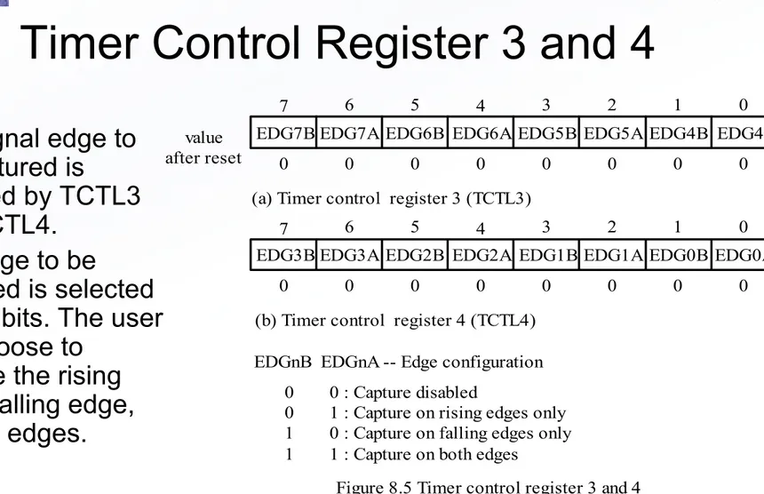
7 6 5 4 3 2 1 0 EDG7B EDG7A EDG6B EDG6A EDG5B EDG5A EDG4B EDG4A value
after reset 0 0 0 0 0 0 0 0
Figure 8.5 Timer control register 3 and 4
7 6 5 4 3 2 1 0 EDG3B EDG3A EDG2B EDG2A EDG1B EDG1A EDG0B EDG0A
0 0 0 0 0 0 0 0 (a) Timer control register 3 (TCTL3)
(b) Timer control register 4 (TCTL4) EDGnB EDGnA -- Edge configuration
0 0 : Capture disabled
0 1 : Capture on rising edges only 1 0 : Capture on falling edges only 1 1 : Capture on both edges
Timer Control Register 3 and 4
• The signal edge to
be captured is
selected by TCTL3
and TCTL4.
• The edge to be
captured is selected
by two bits. The user
can choose to
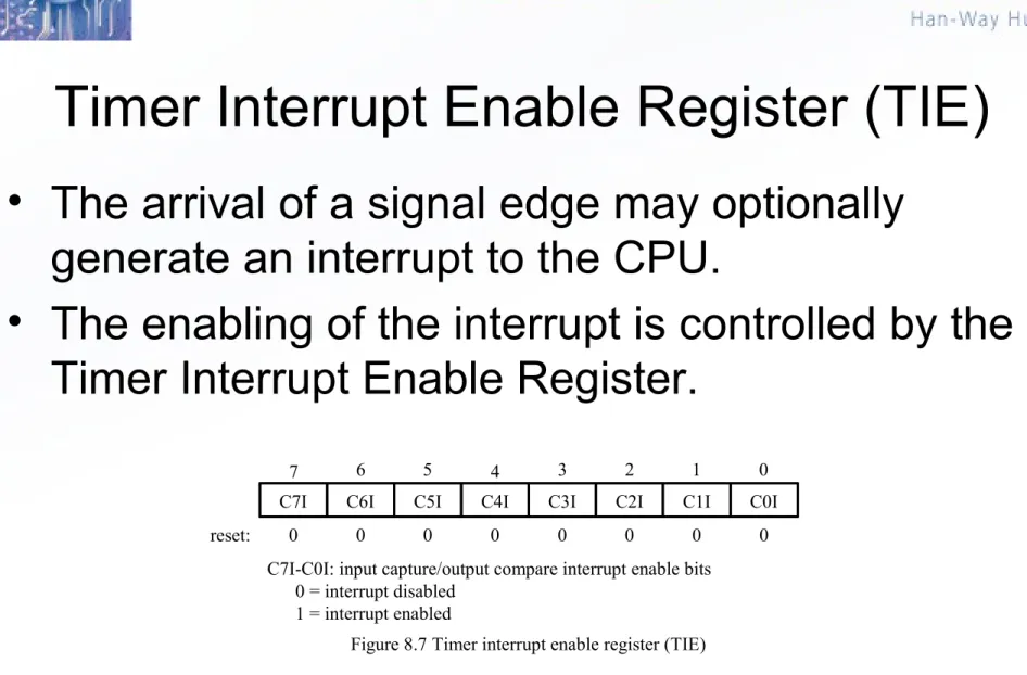
7 6 5 4 3 2 1 0
C7I C6I C5I C4I C3I C2I C1I C0I
reset: 0 0 0 0 0 0 0 0
Figure 8.7 Timer interrupt enable register (TIE) C7I-C0I: input capture/output compare interrupt enable bits 0 = interrupt disabled
1 = interrupt enabled
Timer Interrupt Enable Register (TIE)
• The arrival of a signal edge may optionally
generate an interrupt to the CPU.
7 6 5 4 3 2 1 0
C7F C6F C5F C4F C3F C2F C1F C0F
reset: 0 0 0 0 0 0 0 0
Figure 8.8 Timer interrupt flag register 1 (TFLG1) CnF: input capture/ output compare interrupt flag bits 0 = interrupt condition has not occurred
1 = interrupt condition has occurred
Timer Interrupt Flag 1 Register (TFLG1)
How to Clear a Timer Flag Bit
• In normal mode, write a 1 to the flag bit to be cleared.
• Method 1
– Use the BCLR instruction with a 0 at the bit position (s) corresponding to
the flag (s) to be cleared. For example,
BCLR TFLG1, $FE
will clear the C0F flag.
• Method 2
– Use the movb instruction with a 1 at the bit position (s) corresponding to
the flag (s) to be cleared. For example,
movb
#$01,TFLG1
will clear the C0F flag.
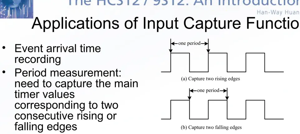
- Pulse width measurement: need to capture the rising and falling edges
one period
(a) Capture two rising edges one period
(b) Capture two falling edges
Figure 8.9 Period measurement by capturing two consecutive edges
Pulse width
Rising edge Falling edge
Figure 8.10 Pulse-width measurement using input capture
Applications of Input Capture Function
• Event arrival time
recording
• Period measurement:
need to capture the main
timer values
- Time reference: often used in conjunction with an output compare function
Start of interval
End of interval e1 e2 e3 e4 ei ej
Figure 8.11 Using an input-capture function for event counting
...
...
Time t0
Time of reference (set up by signal edge)
Time t0 + delay
Time to activate output signal (set up by output compare) Figure 8.12 A time reference application
Input Capture
•
Interrupt generation: Each input capture function can be used as an
edge-sensitive interrupt source.
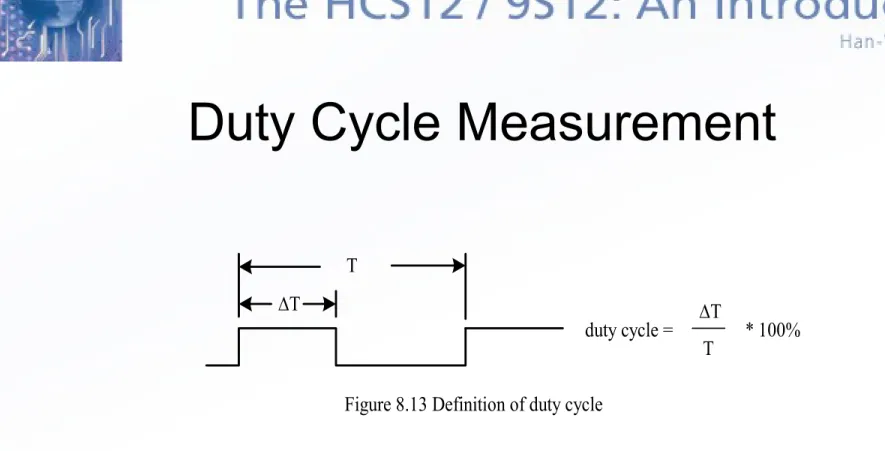
T
T
duty cycle = T
T * 100%
Figure 8.13 Definition of duty cycle
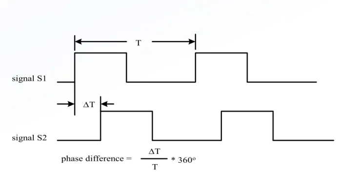
T
T
signal S1
signal S2
phase difference = T
T * 360
o
Figure 8.14 Phase difference definition for two signals
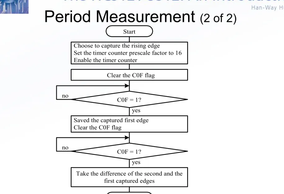
Period Measurement
(1 of 2)
• Example 8.2 Use the IC0 to measure the period of an unknown
signal. The period is known to be shorter than 128 ms. Assume that
the E clock frequency is 24 MHz. Use the number of clock cycles as
the unit of the period.
• Solution:
• Since the input-capture register is 16-bit, the longest period of the
signal that can be measured with the prescaler to TCNT set to 1 is:
216 ÷ 24 MHz = 2.73 ms.
• To measure a period that is equal to 128 ms, we have two options:
– Set the prescale factor to 1 and keep track of the number of times the
timer counter overflows.
– Set the prescale factor to 64 and do not keep track of the number of
times the timer counter overflows.
Start
Choose to capture the rising edge
Set the timer counter prescale factor to 16 Enable the timer counter
Clear the C0F flag
C0F = 1? yes no
Saved the captured first edge Clear the C0F flag
C0F = 1? no
yes
Take the difference of the second and the first captured edges
Stop
Figure 8.16 Logic flow of period measurement program
#include "c:\miniide\hcs12.inc"
org $1000
edge1 ds.b 2 ; memory to hold the first edge
period ds.b 2 ; memory to store the period
org $1500
movb #$90,TSCR1 ; enable timer counter and enable fast timer flags clear
bclr TIOS,IOS0 ; enable input-capture 0
movb #$06,TSCR2 ; disable TCNT overflow interrupt, set prescaler to 64
movb #$01,TCTL4 ; capture the rising edge of PT0 signal
movb #C0F,TFLG1 ; clear the C0F flag
brclr TFLG1,C0F,* ; wait for the arrival of the first rising edge
ldd TC0 ; save the first edge and clear the C0F flag
std edge1
brclr TFLG1,C0F,* ; wait for the arrival of the second edge
ldd TC0
subd edge1 ; compute the period
std period
swi end
#include "c:\egnu091\include\hcs12.h" void main(void)
{
unsigned int edge1, period;
TSCR1 = 0x90; /* enable timer counter, enable fast flag clear*/
TIOS &= ~IOS0; /* enable input-capture 0 /
TSCR2 = 0x06; /* disable TCNT overflow interrupt, set prescaler to 64 */
TCTL4 = 0x01; /* capture the rising edge of the PT0 pin */
TFLG1 = C0F; /* clear the C0F flag */
while (!(TFLG1 & C0F)); /* wait for the arrival of the first rising edge */
edge1 = TC0; /* save the first captured edge and clear C0F flag */
while (!(TFLG1 & C0F)); /* wait for the arrival of the second rising edge */
period = TC0 - edge1;
asm ("swi"); }
Case 1
edge2 edge1
pulse width = ovcnt × 216 + diff
Case 2
edge2 < edge 1
pulse width = (ovcnt – 1) × 216 + diff
•
Example 8.3
Write a program to measure the pulse width of a
signal connected to the PT0 pin. The E clock frequency is 24 MHz.
•
Solution
:
– Set the prescale factor to TCNT to 32. Use clock cycle as the unit of
measurement.
– The pulse width may be longer than 216 clock cycles. We need to keep
track of the number of times that the TCNT timer overflows. Let
• ovcnt = TCNT counter overflow count
• diff = the difference of two consecutive edges
• edge1 = the captured time of the first edge
• edge2 = the captured time of the second edge
#include "c:\miniide\hcs12.inc"
org $1000
edge1 ds.b 2
overflow ds.b 2
pulse_width ds.b 2
org $1500
movw #tov_isr,UserTimerOvf ; set up TCNT overflow interrupt vector
lds #$1500 ; set up stack pointer
movw #0,overflow
movb #$90,TSCR1 ; enable TCNT and fast timer flag clear
movb #$05,TSCR2 ; disable TCNT interrupt, set prescaler to 32
bclr TIOS,IOS0 ; select IC0
movb #$01,TCTL4 ; capture rising edge
movb #C0F,TFLG1 ; clear C0F flag
wait1 brclr TFLG1,C0F,wait1; wait for the first rising edge
movw TC0,edge1 ; save the first edge & clear the C0F flag
movb #TOF,TFLG2 ; clear TOF flag
bset TSCR2,$80 ; enable TCNT overflow interrupt
cli ; "
movb #$02,TCTL4 ; capture the falling edge on PT0 pin
wait2 brclr TFLG1,C0F,wait2; wait for the arrival of the falling edge
ldd TC0
std pulse_width
bcc next ; is the second edge smaller?
ldx overflow ; second edge is smaller, so decrement dex ; overflow count by 1
stx overflow ; "
next swi
tov_isr movb #TOF,TFLG2 ; clear TOF flag
ldx overflow
inx
stx overflow
#include <hcs12.h> #include <vectors12.h>
#define INTERRUPT __attribute__((interrupt))
unsigned diff, edge1, overflow;
unsigned long pulse_width;
void INTERRUPT tovisr(void); void main(void)
{
UserTimerOvf = (unsigned short)&tovisr; overflow = 0;
TSCR1 = 0x90; /* enable timer and fast flag clear */
TSCR2 = 0x05; /* set prescaler to 32, no timer overflow interrupt */
TIOS &= ~IOS0; /* select input-capture 0 */
TCTL4 = 0x01; /* prepare to capture the rising edge */
TFLG1 = C0F; /* clear C0F flag */
while(!(TFLG1 & C0F)); /* wait for the arrival of the rising edge */
TFLG2 = TOF; /* clear TOF flag */
TSCR2 |= 0x80; /* enable TCNT overflow interrupt */ asm("cli");
edge1 = TC0; /* save the first edge */
TCTL4 = 0x02; /* prepare to capture the falling edge */
while (!(TFLG1 & C0F)); /* wait for the arrival of the falling edge */
diff = TC0 - edge1;
if (TC0 < edge1)
overflow -= 1;
pulse_width = overflow * 65536u + diff; asm ("swi");
}
void INTERRUPT tovisr(void) {
TFLG2 = TOF; /* clear TOF flag */
Output Compare Function
• The HCS12 has eight output compare functions.
• Each output compare channel consists of
– A 16-bit comparator
– A 16-bit compare register TCx (also used as inout capture
register)
– An output action pin (PTx, can be pulled high, pulled low, or
toggled)
– An interrupt request circuit
Operation of the Output-Compare Function
(1 of 4)
• One of the applications of the output-compare
function is to trigger an action at a specific time
in the future.
• To use an output-compare function, the user
– Makes a copy of the current contents of the TCNT
register
– Adds to this copy a value equal to the desired delay
– Stores the sum into an output-compare register (TCx,
7 6 5 4 3 2 1 0 OM7 OL7 OM6 OL6 OM5 OL5 OM4 OL4 value
after reset 0 0 0 0 0 0 0 0
read: anytime write: anytime
Figure 8.18 Timer control register 1 and 2 (TCTL1 & TCTL2)
7 6 5 4 3 2 1 0
OM3 OL3 OM2 OL2 OM1 OL1 OM0 OL0
0 0 0 0 0 0 0 0
(a) TCTL1 register
(b) TCTL2 register value
after reset
OMn OLn : output level 0 0 1 1 0 1 0 1
no action (timer disconnected from output pin) toggle OCn pin
clear OCn pin to 0 set OCn pin to high
Operation of the Output-Compare Function
(2 of 4)
• The actions that can be activated on an output compare pin include
– Pull up to high – Pull down to low – Toggle
300 s
700 s
Figure 8.19 1 KHz 30 percent duty cycle waveform
Operation of the Output-Compare Function
(3 of 4)
• A successful compare will set the corresponding flag bit in the
TFLG1 register.
• An interrupt may be optionally requested if the associated interrupt
enable bit in the TIE
register is set.
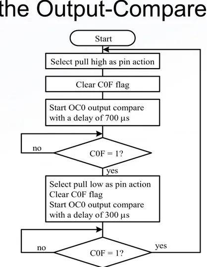
•
Example 8.4
Generate an active high 1 KHz digital waveform with
30 percent duty cycle from the PT0 pin. Use the polling method to
check the success of the output compare operation. The frequency
of the E clock is 24 MHz.
•
Solution:
An active high 1 KHz waveform with 30 percent duty
cycle is shown in Figure 8.19. The logic flow of this problem is
illustrated in Figure 8.20.
Start
Select pull high as pin action
Clear C0F flag
Start OC0 output compare with a delay of 700 s
C0F = 1?
Select pull low as pin action Clear C0F flag
Start OC0 output compare with a delay of 300 s
C0F = 1? no
no
yes
yes
Figure 8.20 The program logic flow for digital waveform generation
#include "c:\miniide\hcs12.inc" hi_time equ 900
lo_time equ 2100 org $1500
movb #$90,TSCR1 ; enable TCNT with fast timer flag clear movb #$03,TSCR2 ; disable TCNT interrupt, set prescaler to 8
bset TIOS,OC0 ; enable OC0
movb #$03,TCTL2 ; select pull high as pin action
ldd TCNT ; start an OC0 operation with 700 us as delay repeat addd #lo_time ; "
std TC0 ; "
low brclr TFLG1,C0F,low ; wait until OC0 pin go high
movb #$02,TCTL2 ; select pull low as pin action
ldd TC0 ; start an OC operation with 300 us as delay addd #hi_time ; "
std TC0 ; "
high brclr TFLG1,C0F,high ; wait until OC0 pin go low movb #$03,TCTL2 ; select pull high as pin action ldd TC0
#include "c:\egnu091\include\hcs12.h" #define hi_time 900
#define lo_time 2100 void main (void)
{
TSCR1 = 0x90; /* enable TCNT and fast timer flag clear */
TIOS |= OC0; /* enable OC0 function */
TSCR2 = 0x03; /* disable TCNT interrupt, set prescaler to 8 */
TCTL2 = 0x03; /* set OC0 action to be pull high */
TC0 = TCNT + lo_time; /* start an OC0 operation */
while(1) {
while(!(TFLG1 & C0F)); /* wait for PT0 to go high */
TCTL2 = 0x02; /* set OC0 pin action to pull low */ TC0 += hi_time; /* start a new OC0 operation */ while(!(TFLG1 & C0F)); /* wait for PT0 pin to go low */
TCTL2 = 0x03; /* set OC0 pin action to pull high */ TC0 += lo_time; /* start a new OC0 operation */ }
}
delayby1ms pshd
movb #$90,TSCR1 ; enable TCNT & fast flags clear
movb #$06,TSCR2 ; configure prescaler to 64
bset TIOS,OC0 ; enable OC0
ldd TCNT
again0 addd #375 ; start an output-compare operation
std TC0 ; with 1 ms time delay
wait_lp0 brclr TFLG1,OC0,wait_lp0
ldd TC0
dbne y,again0
puld rts
•
Example 8.5
Write a function to generate a time delay which is a multiple of
1 ms.
•
Assume that the E clock frequency is 24 MHz. The number of milliseconds
is passed in Y. Also write an instruction sequence to test this function.
•
Solution:
One method to create 1 ms delay is as follows:
– Set the prescaler to TCNT to 64
– Perform the number of output-compare operations (given in Y) with each operation creating a 1-ms time delay.
void delayby1ms(int k) {
int ix;
TSCR1 = 0x90; /* enable TCNT and fast timer flag clear */
TSCR2 = 0x06; /* disable timer interrupt, set prescaler to 64 */
TIOS |= OC0; /* enable OC0 */
TC0 = TCNT + 375;
for (ix = 0; ix < k; ix++) {
while(!(TFLG1 & C0F)); TC0 += 375;
}
#include "c:\MiniIDE\hcs12.inc"
CR equ $0D
LF equ $0A
org $1000
oc_cnt rmb 1
frequency rmb 2
org $1500
movb #$90,TSCR1 ; enable TCNT and fast timer flags clear
movb #$02,TSCR2 ; set prescale factor to 4
movb #$02,TIOS ; enable OC1 and IC0
movb #100,oc_cnt ; prepare to perform 100 OC1 operation, each
; creates 10 ms delay and total 1 second movw #0,frequency ; initialize frequency count to 0
movb #$01,TCTL4 ; prepare to capture the rising edges of PT0
movb #C0F,TFLG1 ; clear the C0F flag
bset TIE,IC0 ; enable IC0 interrupt
cli ; "
•
Example 8.6
Use an input-capture and an output-compare functions to
measure the frequency of the signal connected to the PT0 pin.
•
Solution:
To measure the frequency, we will
– Use one of the output-compare function to create a one-second time base. – Keep track of the number of rising (or falling) edges that arrived at the PT0 pin
ldd TCNT ; start an OC1 operation with 10 ms delay continue addd #60000 ; "
std TC1 ; "
w_lp brclr TFLG1,C1F,w_lp ; wait for 10 ms
ldd TC1
dec oc_cnt
bne continue
ldd frequency
pshd
ldd #msg
jsr [printf,PCR]
leas 2,sp
swi
msg db CR,LF,"The frequency is %d",CR,LF,0
TC0_isr ldd TC0 ; clear C0F flag
ldx frequency ; increment frequency count by 1
inx ; "
stx frequency ;
rti
org $3E6E ; set up interrupt vector number
fdb TC0_isr ; for TC0
#include <hcs12.h> #include <vectors12.h> #include <convert.c> #include <stdio.c>
#define INTERRUPT __attribute__((interrupt)) unsigned int frequency;
void INTERRUPT TC0_isr(void);
void main(void) {
char arr[7];
char *msg = "Signal frequency is "; int i, oc_cnt;
unsigned frequency;
UserTimerCh0 = (unsigned short)&TC0_isr;
TSCR1 = 0x90; /* enable TCNT and fast flag clear */
TSCR2 = 0x02; /* set prescale factor to 4 */
TIOS = 0x02; /* select OC1 and IC0 */
oc_cnt = 100; /* prepare to perform 100 OC1 operations */
frequency = 0;
TCTL4 = 0x01; /* prepare to capture PT0 rising edge */
TFLG1 = C0F; /* clear C0F flag */
TIE |= IC0; /* enable IC0 interrupt */
asm("cli");
TC1 = TCNT + 60000; while (oc_cnt) {
while(!(TFLG1 & C1F)); TC1 = TC1 + 60000; oc_cnt = oc_cnt - 1; }
int2alpha(frequency, arr); puts(msg);
puts(&arr[0]); asm("swi"); }
void INTERRUPT TC0_isr(void) {
TFLG1 = C0F; /* clear C0F flag */
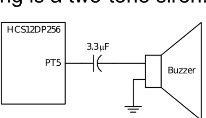
HCS12DP256
PT5
3.3 F
Buzzer
Figure 8.21 Circuit connection for a buzzer
Making Sound Using
the Output-Compare Function
• A sound can be generated by creating a digital waveform
with appropriate frequency and using it to drive a
speaker or a buzzer.
• The circuit connection for a buzzer is shown in Figure
8.21.
Algorithm for Generating a Siren
•
Step 1
– Enable an output compare channel to drive the buzzer (or speaker).
•
Step 2
– Start an output compare operation with a delay count equal to half the period of the siren and enable the OC interrupt.
•
Step 3
– Wait for the duration of the siren tone (say half a second). During the waiting period, interrupts will be requested many times by the output compare function. The interrupt service routine simply restart the output compare operation.
•
Step 4
– At the end of the siren tone duration, choose a different delay count for the output compare operation so that the siren sound may have a different frequency.
•
Step 5
– Wait for the same duration as in Step 3. During this period, many interrupts will be requested by the output compare operation.
•
Step 6
#include "c:\miniide\hcs12.inc"
hi_freq equ 1250 ; delay count for 1200 Hz (with 1:8 prescaler) lo_freq equ 5000 ; delay count for 300 Hz (with 1:8 prescaler)
toggle equ $04 ; value to toggle the TC5 pin
org $1000
delay ds.w 1 ; store the delay for output-compare operation
org $1500
lds #$1500
movw #oc5_isr,UserTimerCh5 ; initialize the interrupt vector entry movb #$90,TSCR1 ; enable TCNT, fast timer flag clear
movb #$03,TSCR2 ; set main timer prescaler to 8
• Example 8.7 Write a program to generate a two-tone
siren that oscillates between 300 Hz and 1200 Hz.
• Solution:
– Set the prescaler to TCNT to 1:8.
– The delay count for the low frequency tone is (24000000
8)
300
2 = 5000.
– The delay count for the high frequency tone is (24000000
8)
bset TIOS,OC5 ; enable OC5
movb #toggle,TCTL1 ; select toggle for OC5 pin action movw #hi_freq,delay ; use high frequency delay count first ldd TCNT ; start the low frequency sound
addd delay ; " std TC5 ; "
bset TIE,OC5 ; enable OC5 interrupt
cli ; "
forever ldy #5 ; wait for half a second jsr delayby100ms ; "
movw #lo_freq,delay ; switch to low frequency delay count
ldy #5
jsr delayby100ms
movw #hi_freq,delay ; switch to high frequency delay count
bra forever
oc5_isr ldd TC5
addd delay
std TC5
rti
#include "c:\egnu091\include\hcs12.h" #include "c:\egnu091\include\delay.c"
#include "c:\egnu091\include\v`ectors12.h"
#define INTERRUPT __attribute__((interrupt))
#define HiFreq 1250
#define LoFreq 5000
int delay; /* delay count for OC5 operation */ void INTERRUPT oc5ISR(void);
int main(void) {
UserTimerCh5 = (unsigned short)&oc5ISR;
TSCR1 = 0x90; /* enable TCNT and fast timer flag clear */ TSCR2 = 0x03; /* set prescaler to TCNT to 1:8 */
TIOS |= BIT5; /* enable OC5 */
TCTL1 = 0x04; /* select toggle for OC5 pin action */ delay = HiFreq; /* use high frequency delay count first */ TC5 = TCNT + delay; /* start an OC5 operation */
TIE |= BIT5; /* enable TC5 interrupt */ asm("cli");
while(1) {
delayby100ms(5); /* wait for half a second */
delay = LoFreq; /* switch to low frequency tone */ delayby100ms(5); /* wait for half a second */
delay = HiFreq; /* switch to high frequency tone */ }
return 0; }
void INTERRUPT oc5ISR(void) {
TC5 += delay; }
Playing Songs Using the OC Function
• Place the frequencies and durations of all notes
in a table.
• For every note, use the output-compare function
to generate the digital waveform with the
specified frequency and duration.
#include "c:\miniide\hcs12.inc"
G3 equ 7653 ; delay count to generate G3 note (with 1:8 prescaler)
B3 equ 6074 ; delay count to generate B3 note (with 1:8 prescaler)
C4 equ 5733 ; delay count to generate C4 note (with 1:8 prescaler)
C4S equ 5412 ; delay count to generate C4S (sharp) note
D4 equ 5108 ; delay count to generate D4 note (with 1:8 prescaler)
E4 equ 4551 ; delay count to generate E4 note (with 1:8 prescaler)
F4 equ 4295 ; delay count to generate F4 note (with 1:8 prescaler)
F4S equ 4054 ; delay count to generate F4S note (with 1:8 prescaler)
G4 equ 3827 ; delay count to generate G4 note (with 1:8 prescaler)
A4 equ 3409 ; delay count to generate A4 note (with 1:8 prescaler)
B4F equ 3218 ; delay count to generate B4F note (with 1:8 prescaler)
B4 equ 3037 ; delay count to generate B4 note (with 1:8 prescaler)
C5 equ 2867 ; delay count to generate C5 note (with 1:8 prescaler)
D5 equ 2554 ; delay count to generate D5 note (with 1:8 prescaler)
E5 equ 2275 ; delay count to generate E5 note (with 1:8 prescaler)
F5 equ 2148 ; delay count to generate F5 note (with 1:8 prescaler)
notes equ 101
org $1000
delay ds.w 1 ; store the delay for output-compare operation
rep_cnt ds.b 1 ; repeat the song this many times
ip ds.b 1 ; remaining notes to be played
org $1500
lds #$1500
; establish the SRAM vector address for OC5
movw #oc5_isr,UserTimerCh5
movb #$90,TSCR1 ; enable TCNT, fast timer flag clear movb #$03,TSCR2 ; set main timer prescaler to 8
bset TIOS,OC5 ; enable OC5
movb #toggle,tctl1 ; select toggle for OC5 pin action
ldx #score ; use as a pointer to score table
ldy #duration ; points to duration table
movb #1,rep_cnt ; play the song twice
movb #notes,ip
movw 2,x+,delay ; start with zeroth note
ldd TCNT ; play the first note
addd delay ; "
std TC5 ; "
forever pshy ; save duration table pointer in stack
ldy 0,y ; get the duration of the current note
jsr delayby10ms ; "
puly ; get the duration pointer from stack
iny ; move the duration pointer
iny ; "
ldd 2,x+ ; get the next note, move pointer
std delay ; "
dec ip
bne forever
dec rep_cnt
beq done ; if not finish playing, re-establish
ldx #score ; pointers and loop count
ldy #duration ; "
movb #notes,ip ; "
movw 0,x,delay ; get the first note delay count
ldd TCNT ; play the first note
addd #delay ; "
std TC5
bra forever
oc5_isr ldd TC5
addd delay
std TC5
rti
; ************************************************************************************ ; The following subroutine creates a time delay which is equal to [Y] times ; 10 ms. The timer prescaler is 1:8.
; ************************************************************************************ delayby10ms
bset TIOS,OC0 ; enable OC0
ldd TCNT
again1 addd #30000 ; start an output-compare operation
std TC0 ; with 10 ms time delay
wait_lp1 brclr TFLG1,C0F,wait_lp1
ldd TC0
dbne y,again1
bclr TIOS,OC0 ; disable OC0
score dw D4,B3,G3,B3,D4,G4,B4,A4,G4,B3,C4S
dw D4,D4,D4,B4,A4,G4,F4S,E4,F4S,G4,G4,D4,B3,G3
dw D4,B3,G3,B3,D4,G4,B4,A4,G4,B3,C4S,D4,D4,D4
dw B4,A4,G4,F4S,E4,F4S,G4,G4,D4,B3,G3,B4,B4
dw B4,C5,D5,D5,C5,B4,A4,B4,C5,C5,C5,B4,A4,G4
dw F4S,E4,F4S,G4,B3,C4S,D4,D4,G4,G4,G4,F4S
dw E4,E4,E4,A4,C5,B4,A4,G4,G4,F4S,D4,D4
dw G4,A4,B4,C5,D5,G4,A4,B4,C5,A4,G4
; ************************************************************************************** ; Each of the following entries multiplied by 10 ms gives the duration of a note. ; **************************************************************************************
duration dw 30,10,40,40,40,80,30,10,40,40,40
dw 80,20,20,60,20,40,80,20,20,40,40,40,40,40
dw 30,10,40,40,40,80,30,10,40,40,40,80,20,20
dw 60,20,40,80,20,20,40,40,40,40,40,20,20
dw 40,40,40,80,20,20,40,40,40,80,40,60,20,40
dw 80,20,20,40,40,40,80,40,40,40,20,20
dw 40,40,40,40,20,20,20,20,40,40,20,20
dw 60,20,20,20,80,20,20,60,20,40,80
#include “c:\egnu091\include\hcs12.h” #include “c:\egnu091\include\vectors12.h”
#define G3 7653 ; delay count to be added to TC5
#define B3 6074 ; to generate the given note
#define C4 5733
#define C4S 5412
#define D4 5108
#define E4 4551
#define F4 4295
#define F4S 4054
#define G4 3827
#define A4 3409
#define B4F 3218
#define B4 3037
#define C5 2867
#define D5 2554
#define E5 2275
#define F5 2148
#define notes 101
#define toggle 0x04
void delayby10ms(int kk);
void INTERRUPT oc5isr(void);
unsigned int score [101] = {D4,B3,G3,B3,D4,G4,B4,A4,G4,B3,C4S, D4,D4,D4,B4,A4,G4,F4S,E4,F4S,G4,G4,D4,B3,G3, D4,B3,G3,B3,D4,G4,B4,A4,G4,B3,C4S,D4,D4,D4, B4,A4,G4,F4S,E4,F4S,G4,G4,D4,B3,G3,B4,B4, B4,C5,D5,D5,C5,B4,A4,B4,C5,C5,C5,B4,A4,G4, F4S,E4,F4S,G4,B3,C4S,D4,D4,G4,G4,G4,F4S, E4,E4,E4,A4,C5,B4,A4,G4,G4,F4S,D4,D4, G4,A4,B4,C5,D5,G4,A4,B4,C5,A4,G4}; unsigned int dur [101] = {30,10,40,40,40,80,30,10,40,40,40, 80,20,20,60,20,40,80,20,20,40,40,40,40,40, 30,10,40,40,40,80,30,10,40,40,40,80,20,20, 60,20,40,80,20,20,40,40,40,40,40,20,20, 40,40,40,80,20,20,40,40,40,80,40,60,20,40, 80,20,20,40,40,40,80,40,40,40,20,20,
main (void) {
int j;
UserTimerCh5 = (unsigned short)&oc5isr;
TSCR1 = 0x90; /* enable TCNT, fast timer flag clear */ TSCR2 = 0x03; /* set TCNT prescaler to 8 */
TFLG1 = 0xFF; /* clear all TxF flags */
TIE |= C5I; /* enable TC5 interrupt */
TIOS |= OC5; /* enable OC5 function */
TCTL1 = toggle; /* select toggle as OC5 pin action */ asm(" cli "); /* enable TC5 interrupt */
j = 0;
delay = score[0];
TC5 = TCNT + delay; /* play the first note */ while (j < notes) { /* play the song once */ delay = score[j]; /* play the jth note */ delayby10ms(dur[j]);
j++;
}
TIOS &= ~OC5; /* stop playing the song */
void delayby10ms(int kk) {
int i;
TIOS |= OC0; /* enable OC0 */
TC0 = TCNT + 30000; /* start one OC0 operation */ for (i = 0; i < kk; i++) {
while(!(TFLG1 & C0F));
TC0 += 30000;
}
TIOS &= ~OC0; }
void INTERRUPT oc5isr(void) {
Drawback of the Song Algorithm
• Contiguous identical notes become one note
7 6 5 4 3 2 1 0
reset 0 0 0 0 0 0 0 0
OC7M7 OC7M6 OC7M5 OC7M4 OC7M3 OC7M2 OC7M1 OC7M0
OC7Mn n = 0..7
0 = PTn pin is not affected by OC7 function
1 = A successful OC7 action will override a successful OC6-OC0 compare action during the same cycle and the OCn action taken will depend on the corresponding OC7D bit.
Figure 8.22 Output Compare 7 Mask Register (OC7M)
7 6 5 4 3 2 1 0
reset 0 0 0 0 0 0 0 0
OC7D7 OC7D6 OC7D5 OC7D4 OC7D3 OC7D2 OC7D1 OC7D0
Figure 8.23 Output Compare 7 Data Register (OC7D)
Using OC7 to Control Multiple OC Functions
•
OC7 can control up to eight channels of OC functions.
•
The register OC7M specifies which OC channels are controlled by OC7.
•
The register OC7D specifies the value that any PTx pin to assume when the
OC7 operation succeeds.
• Example 8.9 What value should be written into OC7M
and OC7D if one wants pins PT2, PT3, and PT4 to
assume the values of 1, 0, and 1, respectively when
OC7 compare succeeds?
• Solution:
– 4, 3, and 2 of OC7M must be set to 1, and bits 4, 3, 2, of OC7D
should be set to 1, 0, and 1, respectively.
– The following instruction sequence will achieve the desired
effect:
7 6 5 4 3 2 1 0
reset: 0 0 0 0 0 0 0 0
FOC7 FOC6 FOC5 FOC4 FOC3 FOC2 FOC1 FOC0
Figure 8.24 Contents of the CFORC register
Forced Output-Compare
(1 of 2)
• There are applications in which the user wants an output
compare in action to occur immediately instead of
waiting for a match between the TCNT and the proper
output compare register.
• This situation arises in the spark plug timing control and
some automotive engine control applications.
• To force an output compare operation, write ones to the
corresponding bit in the CFORC register.
• At the next timer count after the write to the CFORC
register, the forced channels will trigger their
Table 8.2 Pin actions on PT7-PT0 pins
Register Bit positions Value Action to be triggered TCTL1
TCTL2
7 6 5 4 3 2 1 0 7 6 5 4 3 2 1 0
1 1 0 1 0 1 1 0 0 1 1 0 1 1 1 0
set the PT7 pin to high toggle the PT6 pin toggle the PT5 pin pull the PT4 pin to low toggle the PT3 pin pull the PT2 pin to low set the PT1 pin to high pull the PT0 pin to low
Forced Output-Compare
(2 of 2)
• Example 8.12 Suppose that the contents of the TCTL1 and TCTL2
registers are $D6 and $6E, respectively. The contents of the TFLG1
are $00. What would occur on pins PT7 to PT0 on the next clock
cycle if the value $7F is written into the CFORC register?
• Solution:
– The TCTL1 and TCTL2 configure the output-compare actions as shown
in Table8.2.
– The TFLG1 register indicates that none of the started output-compare
operations have succeeded yet.
Pulse Accumulator
•
The HCS12 standard timer system has a 16-bit pulse accumulator PACA.
•
The HCS12 ECT system has four 8-bit pulse accumulators (PAC3…PAC0).
•
Two adjacent 8-bit pulse accumulators can be concatenated into a 16-bit
pulse accumulator.
•
PAC3 and PAC2 can be concatenated into the 16-bit PACA whereas PAC1
and PAC0 can be concatenated into the 16-bit PACB.
•
There are four possible pulse accumulator configurations:
– Two 16-bit pulse accumulators PACA and PACB
– One 16-bit pulse accumulator PACA and two 8-bit pulse accumulators PAC1 and PAC0
– One 16-bit pulse accumulator PACB and two 8-bit pulse accumulators PAC3 and PAC2
– Four 8-bit accumulators PAC3~PAC0
– Four 8-bit pulse accumulators PAC3…PAC0 are sharing the signal pins PT3… PT0.
H os t C P U d at a bu s
edge detector delay counter PT0 8-bit PAC0 (PACN0) EDG0 PA0H holding register 0
edge detector delay counter PT1 8-bit PAC1 (PACN1) EDG1 PA1H holding register 0
edge detector delay counter PT2 8-bit PAC2 (PACN2) EDG2 PA2H holding register 0
edge detector delay counter PT3 8-bit PAC3 (PACN3) EDG3 PA3H holding register 0 interrupt interrupt Load holding register and reset pulse accumulator
In te rm od ul e B us 4:1 Mux CLK1 CLK0 prescaled clock from timer
timer clock (TIMCLK)
8-bit PAC3 (PACN3) 8-bit PAC2 (PACN2) PA C L K ÷ 6 55 36 PA C L K ÷ 2 56 MUX edge detector PT7
÷ 64 M clock clock select (PAMOD) interrupt PACA 8-bit PAC1 (PACN1) 8-bit PAC0 (PACN0) PACB interrupt delay counter
edge detector PT0
Figure 8.26 16-bit Pulse accumulator block diagram
PA
C
L
Pulse Accumulator Operation Modes
• Event counting mode. The 16-bit PACA can operate in
this mode and count the number of events arrived at the
PT7 pin. The 16-bit PACB and all four 8-bit pulse
accumulators can operate only in this mode.
• Gated accumulation mode. The 16-bit PACA can also
operate in this mode. As long as the PT7 signal is active
(can be high or low), the PACA counter is clocked by a
free-running E
64 signal.
• The active edge of the PACB and PAC3…PAC0 are
identical to those of IC0 and IC3…IC0, respectively.
Interrupt Sources for Pulse Accumulators
• The 16-bit PACA has two interrupt sources:
PT7-edge and PACA counter overflow.
• Only two (PAC3 and PAC1) of the 8-bit pulse
accumulators can generate interrupt.
– These two pulse accumulators can interrupt whenever
their counters overflow.
Registers Related to Pulse Accumulators
• The operation of the 16-bit PACA is controlled by the PACTL
register. The contents of this register are shown in Figure 8.27.
• PACA has a 16-bit counter which comprises of PAC3 and PAC2.
This 16-bit counter can be accessed by using the name PACNT.
• The status of the PACA is recorded in the PAFLG register.
• The operation of the PACB is controlled by the PBCTL register.
• The status of PACB is recorded in the PBFLG register.
• Each of the 8-bit pulse accumulators can be enabled by setting a
proper bit in the ICPAR register.
• Each of the 8-bit pulse accumulator also has a holding register
(PA3H…PA0H).
7 6 5 4 3 2 1 0
reset: 0 0 0 0 0 0 0 0
0 PAEN PAMOD PEDGE CLK1 CLK0 PAOVI PAI
Figure 8.27 Pulse accumulator control register (PACTL)
PAEN -- Pulse accumulator system enable bit
0 = PACA is disabled (PACN3 and PACN2 can be enabled) 1 = PACA is enabled (PACN3 and PACN2 cannot be enabled) PAMOD -- Pulse accumulator mode bit
0 = event counter mode
1 = gated time accumulation mode
PEDGE -- Pulse accumulator edge control bit For PAMOD = 0 (event counter mode)
0 = falling edges on the PAI pin cause the count to increment 1 = rising edges on the PAI pin cause the count to decrement For PAMOD = 1 (gated time accumulation mode)
0 = PAI pin high enables E÷64 clock to pulse accumulator and the trailing falling edge on the PAI pin sets the PAIF flag 1 = PAI pin low enables E÷64 clock to pulse accumulator and
the trailing rising edge on the PAI pin sets the PAIF flag CLK1 and CLK0 -- Clock select bits
00 = use timer prescaler clock as timer counter clock 01 = use PACLK as input to timer counter (TCNT) clock 10 = use PACLK/256 as timer counter clock
11 = use PACLK/65536 as timer counter clock
PAOVI -- Pulse accumulator overflow interrupt enable bit 0 = disable
1 = enable
PAI -- PAI pin interrupt enable bit 0 = disabled
7 6 5 4 3 2 1 0
reset: 0 0 0 0 0 0 0 0
0 0 0 0 0 0 PAOVF PAIF
Figure 8.28 Pulse accumulator flag register (PAFLG)
PAOVF -- pulse accumulator overflow flag
This flag is set when PACNT overflows from $FFFF to $0000 and can be cleared by writing a 1 to it.
PAIF -- PT7 pin edge flag
When in event counter mode, this bit is set when the selected edge on the PT7 pin is detected.
When in gated accumulator mode, the selected trailing edge sets this flag.
7 6 5 4 3 2 1 0
reset: 0 0 0 0 0 0 0 0
0 PA3EN PA2EN PA1EN
0 0 0 PA0EN
Figure 8.30 Input control pulse accumulator control register (ICPACR) PAxEN -- 8-bit pulse accumulator x enable bit
7 6 5 4 3 2 1 0
reset: 0 0 0 0 0 0 0 0
0 0 0 PBOVI
0 PBEN 0 0
(a) Pulse accumulator B control register (PBCTL) PBEN -- Pulse accumulator B system enable bit
0 = 16-bit pulse accumulator disabled. Eight-bit PAC1 and PAC0 can be enabled when their related enable bits in ICPACR are set. 1 = pulse accumulator B system enabled.
PBOVI -- Pulse accumulator B overflow interrupt enable bit 0 = interrupt inhibited.
1 = interrupt requested if PBOVF is set
7 6 5 4 3 2 1 0
0 0 0 0 0 0 0 0
0 0 0 PBOVF
0 0 0 0
reset:
PBOVF -- Pulse accumulator B overflow flag
This bit is set when the 16-bit pulse accumulator B overflows from $FFFF to $0000 or when 8-bit accumulator 1 (PAC1) overflows from $FF to $00. It is clearded by writing 1 to it or by accessing PACN1 and PACN0 when the TFFCA bit in the TSCR register is set. (b) Pulse accumulator B flag register (PBFLG)
7 6 5 4 3 2 1 0
reset: 0 0 0 0 0 0 0 0
SH04 TFMOD PACMX BUFEN
SH37 SH26 SH15 LATQ
SHxy -- share input action of input capture channel x and y bits 0 = normal operation
1 = The channel input x causes the same action on the channel y. TFMOD -- timer flag-setting mode bit
0 = The timer flags C3F-C0F in TFLG1 are set when a valid input capture transition on the corresponding port pin occurs. 1 = If in queue mode (BUFEN = 1 and LATQ = 0), the timer flags C3F-C0F in TFLG1 are set only when a latch on the
corresponding holding register occurs. If the queue mode is not engaged, the timer flags C3F-C0F are set the same way as for TFMOD = 0.
PACMX -- 8-bit pulse accumulator maximum count bit
0 = normal operation. When the 8-bit pulse accumulator has reached the value $FF, with the next active edge, it will be incremented to $00.
1 = When the 8-bit pulse accumulator has reached the value $FF, it will not be incremented further. The value $FF indicates a count of 255 or more.
BUFEN -- IC buffer enable bit
0 = input capture and pulse accumulator holding registers are disabled.
1 = input capture and pulse accumulator holding registers are enabled.
LATQ -- input capture latch or queue mode select bit
The BUFEN bit should be set to enable IC and pulse accumulator's holding registers. Otherwise, LATQ latching mode is disabled. 0 = queue mode of input capture is enabled
1 = latch mode is enabled. Latching function occurs when modulus down-counter reaches 0 or a 0 is written into the count register MCCNT. With a latching event, the contents of IC registers and 8-bit pulse accumulators are transferred to their holding registers. The 8-bit pulse accumulators are cleared.
#include "c:\miniide\hcs12.inc"
N equ 1350
org $1500
lds #$1500 ; set up stack pointer
movw #paov_isr,UserPAccOvf ; set up PAOV interrupt vector
ldd #N ; place the 2s complement in PACNT
coma ; “
comb ; “
addd #1 ; “
std PACNT ; “
movb #$52,PACTL ; enable PACA, event counting mode, active
; edge is rising
cli ; enable PAOV interrupt
; …
swi
paov_isr movb #PAOVF,PAFLG ; clear the PAOVF flag
end
• Example 8.13 Suppose that certain events are converted into pulses and connected to the PT7 pin. Write a program that enables the PACA to generate an interrupt to the MCU when N events have occurred.
#include “c:\egnu091\include\hcs12.h” #include “c:\egnu091\include\vectors12.h”
#define N 1252
#define INTERRUPT __attribute__((interrupt))
void INTERRUPT paov_isr (void);
void main(void) {
UserPAccOvf = (unsigned short)&paov_isr;
PACNT = ~N + 1; /* load the 2’s complement of N into PACNT */ PACTL = 0x52;
asm("cli"); /* enable PAOV interrupt */ ....
}
void INTERRUPT paov_isr(void) {
PAFLG = PAOVF;
}
Procedure for Measuring Signal Frequency
Using the PA Function
• Step 1
– Connect the signal to the PT7 pin.
• Step 2
– Set up the PACA to operate in event counting mode.
• Step 3
– Use one of the output-compare functions to create a 1-second time interval or call the library delay function. (Or use the modulus down counter).
• Step 4
– Use a memory location to keep track of the number of times that the PACNT overflows.
• Step 5
– Enable the PAOV interrupt.
• Step 6
– Disable the PAOV interrupt at the end of one second.
• The frequency of the unknown signal is given by the following equation:
frequency = paov_cnt × 216 + PACNT
#include "c:\miniide\hcs12.inc"
org $1000
oc_cnt rmb 1
paov_cnt rmb 2 ; use to keep track of PACNT overflow count
frequency rmb 4 ; hold the signal frequency
org $1500
lds #$1500
movw #paov_isr,UserPAccOvf ; set up PAOV interrupt vector
movb #50,oc_cnt ; prepare to perform 50 OC0 actions
ldd #0
std PACNT ; let PACNT count up from 0
std paov_cnt ; initialize PACNT overflow count to 0
std frequency ; initialize frequency to 0
std frequency+2 ; "
movb #$90,TSCR1 ; enable TCNT and fast timer flag clear
bset TIOS,OC0 ; select OC0 function
movb #$03,TSCR2 ; set prescaler to TCNT to 8
bclr DDRT,$80 ; configure PT7 for input
; configure PA function: enable PA, select event counting mode, rising edge ; of PAI signal increments the PACNT counter, enable PAOV interrupt
movb #$52,PACTL
cli ; enable PAOV interrupt
sec_loop addd #60000
std TC0
brclr TFLG1,C0F,* ; wait for 20 ms here
ldd TC0
dec oc_cnt
bne sec_loop
movb #0,PACTL ; disable PA function
sei ; disable interrupt
ldd PACNT
std frequency+2
ldd paov_cnt
std frequency
swi
paov_isr movb #PAOVF,PAFLG ; clear the PAOVF flag
ldx paov_cnt ; increment PACNT overflow
inx ; count by 1
stx paov_cnt ; "
#include “c:\egnu091\include\hcs12.h” #include “c:\egnu091\include\vectors12.h”
#define INTERRUPT __attribute__((interrupt)) unsigned long int frequency;
unsigned int paov_cnt;
void INTERRUPT paov_isr (void); void main (void)
{
int oc_cnt;
UserPAccOvf = (unsigned short)&paov_isr; PACNT = 0;
frequency = 0; paov_cnt = 0;
TSCR1 = 0x90; /* enable TCNT and fast flag clear */ TIOS = OC0; /* select OC0 function */
TSCR2 = 0x03; /* set prescale factor to 8 */
PACTL = 0x52; /* enable PA function, enable PAOV interrupt */ DDRT &= 0x7F; /* configure the PT7 pin for input */
asm("cli"); /* enable interrupt globally */ oc_cnt = 50;
TC0 = TCNT + 60000u;
while (oc_cnt) {
while(!(TFLG1 & C0F)); TC0 = TC0 + 60000u; oc_cnt --;
}
PACTL = 0x00; /* disable PA function */
asm("sei"); /* disable interrupt */
frequency = (long)paov_cnt * 65536l + (long)PACNT; asm("swi");
}
void INTERRUPT paov_isr (void) {
PAFLG = PAOVF; /* clear PAOVF flag */
paov_cnt = paov_cnt + 1;
Using the PA Function
to Measure Pulse Duration
•
Step 1
– Select gated time accumulation mode, and initialize PACNT to 0.
•
Step 2
– Select the falling edge as the active edge, which will enable TACNT to count when the PAI pin is high.
•
Step 3
– Enable the PAI active edge interrupt and wait for the arrival of the active edge of PAI.
•
Step 4
– Stop the pulse accumulator counter when the interrupt arrives.
•
To measure long pulse, we need to keep track of PA overflow:
pulse_width = [(216 × paov_cnt) + PACNT] × 64TE
•
Example 8.13 Write a program to measure the duration of an unknown
signal connected to the PAI pin.
#include "c:\miniide\hcs12.inc"
org $1000
paov_cnt ds.b 1 ; use to keep track of the PACNT overflow count
pulse_width ds.b 3 ; hold the pulse width
org $1500
movw #paov_isr,UserPAccOvf ; set up PAOV interrupt vector
ldd #0
std PACNT ; let PACNT count up from 0
clr paov_cnt ; initialize PACNT overflow count to 0
movb #$0,TSCR2 ; set TCNT timer prescaler to 1
movb #$72,PACTL
bclr DDRT,$80 ; configure PAI pin for input
cli ; enable PAOV interrupt
brclr PAFLG,PAIF,* ; wait for the arrival of the falling edge of PAI
movb #0,PACTL ; disable PA function
sei ; disable interrupt
ldd PACNT
std pulse_width+1
ldaa paov_cnt
staa pulse_width
paovISR movb #PAOVF,PAFLG
inc paov_cnt
Modulus Down-Counter
• Can generate periodic interrupts
• Can be used to latch the value of IC registers and the pulse
accumulators to their holding registers.
• The action of latching can be periodic or only once.
• The clock input (E clock) to the modulus down counter is prescaled
by 1, 4, 8, or 16.
• The operation of the modulus down counter is controlled by the
MCCTL register and the status of its operation is recorded in the
MCFLG register.
• The modulus down counter MCCNT is 16-bit.
• The MCCNT register has a 16-bit load register, which will be
reloaded into MCCNT when it decrements to 0.
7 6 5 4 3 2 1 0
reset: 0 0 0 0 0 0 0 0
ICLAT FLMC MCEN MCPR1
MCZI MODMC RDMCL MCPR0
Figure 8.32 Modulus down-counter control register (MCCTL) MCZI -- modulus counter underflow interrupt enable bit
0 = modulus counter underflow interrupt is disabled 1 = modulus counter underflow interrupt is enabled MODMC -- modulus mode enable bit
0 = the counter counts once from the value written to it and will stop at $0000. 1 = modulus mode is enabled. When the counter reaches $0000, the counter is loaded with the latest value written into to the modulus count register. RDMCL -- read modulus down-counter load bit
0 = reads of the modulus count register will return the present value of the count register.
1 = reads of the modulus count register will return the contents of the load register (i.e., the reload value is returned)
ICLAT -- input capture force latch action bit
This bit has effect only when both the LATQ and BUFEN bits in ICSYS are set. 0 = no effect
1 = forces the contents of the input capture registers TC0 to TC3 and their
corresponding 8-bit pulse accumulators to be latched into the associated holding registers. The pulse accumulators will be cleared when the latch action occurs. FLMC -- force load register into the modulus counter count register bit
This bit has effect only when MCEN = 1. 0 = no effect
1 = loads the load register into the modulus counter count register. This also resets the modulus counter prescaler.
MCEN -- modulus down-counter enable bit
0 = modulus counter is disabled and preset to $FFFF 1 = modulus counter is enabled
MCPR1 & MCPR0 -- modulus counter prescaler select bits 0 0 = prescale rate is 1
7 6 5 4 3 2 1 0
reset: 0 0 0 0 0 0 0 0
0 POLF3 POLF2 POLF1
MCZF 0 0 POLF0
Figure 8.33 Modulus down-counter flag register (MCFLG) MCZF -- modulus counter underflow interrupt flag
This flag is set when the modulus down-counter reaches 0. Writing 1 to this bit clears the flag.
POLF3-POLF0 -- first input capture polarity status bits
These are read-only bits. Writing to these bits has no effect. Each status bit gives the polarity of the first edge which has caused an input capture to occur after capture latch has been read.
movb #$C7,MCCTL
movw #15000,MCCNT ; place the value that will be decremented to
; to 0 in 10 ms
cli ; enable interrupt
• Example 8.17 Write an instruction sequence to generate
periodic interrupt every 10 ms.
• Solution: One possible value to be written into the
MCCTL register is $C0 which will:
– Enable MCCNT
– Enable MCCNT interrupt
– Enable modulus mode
– Set prescaler to 16
delayby10ms
bset TSCR1,TFFCA ; enable timer fast flag clear
movb #$07,MCCTL ; enable modulus down counter with 1:16 as
prescaler
movw #15000,MCCNT ; load the value to be down counted
brclr MCFLG,MCZF,*
bclr MCCTL,$04 ; disable modulus down counter
dbne y,delay10ms
rts
• Time delays equal to a multiple of 10 ms, 50 ms, 1 ms, 100ms, and 1s can be created by modifying this subroutine.
• These six delay functions are placed in the file delay.asm and delay.c and can be included in user’s program.
Using Modulus Down Counter to
Generate Time Delay
• It is most convenient to use the non-modulus mode to create time delay.
• Example 8.18 Write a subroutine to create a time delay that is a multiple of 10 ms using the modulus down counter. The multiple is passed in Y. E clock is 24 MHz. • Solution: By setting the prescaler to 16, the value of 15000 will take 10 ms to
7 6 5 4 3 2 1 0
reset: 0 0 0 0 0 0 0 0
NOVW4 NOVW3 NOVW2 NOVW1
NOVW7 NOVW6 NOVW5 NOVW0
NOVWn: No input capture overwrite
0 = The contents of the related capture register or holding register can be overwritten when a new input capture or latch occurs.
1 = The related capture register or holding register cannot be written by an event unless they are empty. This will prevent the captured value to be overwritten until it is read or latched in the holding register.
Figure 8.34 Input control overwrite register (ICOVW)
Enhanced Capture Timer (ECT)
• Has all the features provided in the standard timer module
• Has one 16-bit holding register for each of the four input-capture
(IC) channels IC3…IC0
• The holding register option is controlled by the ICOVW register.
• Has four 8-bit pulse accumulators
• Has a 16-bit modulus down counter
Why Enhanced Capture Timer?
• Suitable for high-frequency operation (MCU
does not need to read the first edge before the
second edge arrives).
• Simplifies software for signal measurement
Operation of the Enhanced Capture Timer
• A holding register is empty if its value has been read.
• The ECT module can be configured in latch mode or queue mode.
• In latch mode, latching is done when the modulus down counter
reaches 0 or a zero is written into MCCNT.
• During the latching event, the contents of IC registers and the 8-bit
pulse accumulators are transferred to their holding registers. After
this, the pulse accumulators are cleared.
• In queue mode, the main timer value is copied into the TCx register
by a valid input pin transition. With a new capture, the contents of
the TCx register will be transferred to its holding register.
Prescaler 16-bit free-running main timer
pin logic Delay
counter
comparator TCx capture/compare
register
TCxH hold register
EDG x
Prescaler bus clock
÷1, 4, 8, 16
÷1,2,...,128 16-bit load register
16-bit modulus down counter
ICLAT, LATQ, BUFEN (force latch)
write $0000 to modulus counter
LATQ (MDC latch enable)
L
at
ch
Figure 8.35 Enhanced Input capture function block diagram in latch mode to other IC channels
bus clock
PTx
one IC channel (IC0..IC3) pin logic PTi comparator TCx capture/compare register MUX EDG i EDG j
j = 8 - i
Prescaler 16-bit free-running main timer
pin logic Delay
counter
comparator TCx capture/compare
register
TCxH hold register
EDG x
Prescaler bus clock
÷1, 4, 8, 16
÷1,2,...,128 16-bit load register
16-bit modulus down counter
Figure 8.36 Enhanced Input capture function block diagram in Queue mode (channels IC0..IC3 block diagram)
to other IC channels bus clock
PTx
one IC channel (IC0..IC3) pin logic PTi comparator TCx capture/compare register MUX
EDG i EDG j
j = 8 - i
7 6 5 4 3 2 1 0
reset: 0 0 0 0 0 0 0 0
0 0 0 DLY1
0 0 0 DLY0
Figure 8.37 Delay counter control register (DLYCT) DLYx -- delay counter select bits
0 0 -- disabled (bypassed) 0 1 -- 256 P clock cycles 1 0 -- 512 P clock cycles 1 1 -- 1024 P clock cycles
True Edge Detection
• The ECT module uses a delay counter to distinguish true edge and
false.
• A transition is determined to be a true edge if the transition is longer
than the preset duration.
#include "c:\miniide\hcs12.inc" org $1000
period ds.w 1 ; memory to store the period org $1500
movb #$90,TSCR ; enable timer counter and fast timer flag clear bclr TIOS,IOS0 ; enable input-capture 0
movb #$04,TSCR2 ; disable TCNT overflow interrupt, set prescale ; factor to 16
movb #$01,TCTL4 ; choose to capture the rising edge of PT0 pin
movb #$0A,ICSYS ; enable timer flag-setting, IC buffer, and queue mode clr DLYCT ; disable delay counter
bset ICOVW,NOVW0 ; no input-capture overwrite for IC0 ldd TC0 ; empty the input-capture register TC0 ldd TC0H ; empty the holding register TC0H
brclr TFLG1,$FE,* ; wait for the arrival of the second rising edge ldd TC0
subd TC0H ; subtract the first edge from the second edge std period
swi end
•
Example 8.19 Write a program to measure the period of an unknown signal
connected to the PT0 pin using the enhanced capture feature of ECT.
#include “c:\egnu091\include\hcs12.h” void main(void)
{
unsigned int period;
TSCR1 = 0x90; /* enable timer counter, enable fast timer flag clear*/
TIOS &= ~IOS0; /* enable input-capture 0 */
TSCR2 = 0x04; /* set prescale factor to 16 */
TCTL4 = 0x01; /* capture the rising edge of PT0 pin */
/* enable timer flag-setting mode, IC buffer, and queue mode */
ICSYS = 0x0A;
DLYCT = 0x00; /* disable delay counter */
ICOVW |= NOVW0; /* disable input-capture overwrite */
period = TC0; /* empty TC0 and clear the C0F flag */
period = TC0H; /* empty the TC0H register */
/* wait for the arrival of the second rising edge */ while (!(TFLG1 & C0F));
period = TC0 - TC0H;
#include "c:\miniide\hcs12.inc"
org $1000
edge1 rmb 2
overflow rmb 2
pulse_width rmb 2
org $1500
movw #tov_isr,UserTimerOvf ; set up timer overflow interrupt vector
ldd #0
std overflow
movb #$90,TSCR1 ; enable TCNT and fast timer flag clear
movb #$04,TSCR2 ; set prescaler to TCNT to 16
bclr TIOS,IOS0 ; enable input-capture 0
movb #$01,DLYCT ; set delay count to 256 E cycles
movb #$01,ICOVW ; prohibit overwrite to TC0 register
movb #$0,ICSYS ; disable queue mode
movb #$01,TCTL4 ; capture the rising edge on PT0 pin
• Example 8.20 Write a program to measure the pulse width of a
signal connected to the PT0 pin in a noisy environment. Ignore any
noise pulse shorter than 256 P clock cycles.
movb #C0F,TFLG1 ; clear C0F flag
brclr TFLG1,C0F,* ; wait for the arrival of the first rising edge
movb #TOF,TFLG2 ; clear the TOF flag
bset TSCR2,TOI ; enable TCNT overflow interrupt
cli ; "
movw TC0,edge1 ; clear C0F flag and save the captured first edge
movb #$02,TCTL4 ; capture the falling edge on PT0 pin
brclr TFLG1,C0F,* ; wait for the arrival of the falling edge
ldd TC0
subd edge1
std pulse_width
bcc next
; second edge is smaller, so decrement overflow count by 1
ldx overflow
dex
stx overflow
next swi
tov_isr movb #TOF,TFLG2 ; clear TOF flag
ldx overflow ; increment TCNT overflow count
inx ; "
stx overflow ; "