ECE331 Lab #1 Fall 2010: CSMB12C128 Microcontroller Module, USB
BDM Debugger, Code Warrior IDE, and a Fair Dice Tossing Program
________________________________________________________________________________
Keith Hoover and Jianjian Song
Department of Electrical and Computer Engineering
Rose-Hulman Institute of Technology
Revised August 2010
1 Introduction and Precautions...2
2 Objectives...3
3 Deliverable...3
4 Reference materials (Please download the entire Lab 1 folder as well as the 9S12C128 PDF Documents folder from the ECE331 class AFS folder)...4
4.1 Equipment... 4
4.2 Software Installation... 4
5 Mounting your CSMB12C128 module on the project board and interfacing a pushbutton switch and an LED...5
6 Our first assembly language example: A computer-controlled flashlight...8
6.1 Use of CodeWarrior IDE to assemble the flashlight program...8
6.1.1 Launch CodeWarrior IDE... 8
6.1.2 Create New Project... 8
6.1.3 Entering the flashlight assembly source program...9
6.1.4 Building the project... 11
6.1.5 Motorola S-Record Absolute (ASCII Text) Machine Code File Format...12
6.1.6 Assembly Listing File... 13
7 CodeWarrior Simulator: program debugging without the CSMB12C128 module...13
8 Using the CodeWarrior In-Circuit Background Debugger (BDM)...14
8.1 Preparation before launching the BDM debugger...15
8.2 Using the CodeWarrior IDE with the BDM debug monitor...15
8.3 Debugging with the in-circuit debugger...15
8.4 Stand-alone execution of the user program...16
9 Second assembly language example: Coin-Tossing Program...16
9.1 Coin-Tossing Program Specification...16
9.2 Charting your course: the program flowchart...16
9.3 Writing the actual program...20
9.4 Making the project and using the BDM debugger...20
9.5 Debugging without the CSMB12C128 Hardware: using the Simulator...20
10 Your first embedded design assignment: A “fair” dice tosser!...21
11 Possible Errors and Solutions...22
11.1 Elf Loader Error... 22
11.2 Simulator RAM range error...22
11.3 Error message: L1116: Function main not found...23
11.4 Error in command file .\cmd\monitor_postload.cmd!...23
1
Introduction and Precautions
In this lab you will gain familiarity with the CodeWarrior IDE (integrated
development environment) and you will write your first 9S12C128 assembly language program. We are going to go through a lot in this first lab, and you will need to follow the directions carefully in order to be successful. Though you should work individually and turn in individual lab reports, you should work “loosely” with your lab partner when you are having trouble with any part of this lab. You should help each other when one of you is stuck.
Each student must buy a CSMB12C128 microcontroller module (manufactured by Axiom for Freescale), along with a small kit of parts that will be used in the lab work. In addition, you will be checking out a “project board microcontroller unit student
learning kit” (PBMCUSLK), which you will be responsible for over the upcoming quarter (the cost of this board if it is damaged or lost is $200.00). The CSMB12C128 module can be used independently of the PBMCUSLK project board, however the PBMCUSLK project board provides a convenient way of making connections to the microcontroller module via a 60-pin IDE header, and also the project board has additional switches, lights, and other I/O capabilities not found on the microcontroller module. We ask that each student buy the CSMB12C128 microcontroller module, because it’s I/O pins are easily damaged if you are careless. The 9S12C128 microcontroller chip on board the CSMB12C128 module has limited current sourcing and sinking capability (on the order of 20 mA). Therefore a switching transistor should be used to drive high current loads (such as a motor or solenoid) which draw current in excess of 20 mA.
Please exercise reasonable caution in guarding against electrostatic discharge (ESD) damage to your module, as well as to the project board. This means that you should always keep your PBMCUSLK project board in the pink polyethylene ESD protection bag when you are not using it (you may keep the CSMB12C128
microcontroller module plugged into this board and thus store it in the bag as well). Also be careful to touch a grounded object (such as an oscilloscope chassis) to discharge any built up static charges on your body to ground before you touch the project board or the microcontroller module.
Take care to turn the dc power off (this means to unplug the USB cable that is connected to the project board) before adding or modifying any wiring to your board, or before you plug in or unplug your CSMB12C128 microcontroller module to/from the project board.
When wiring circuits on the project board, please follow the ten rules listed below for a “happy, healthy” breadboard board. By now, these rules should be common-sense, as they apply to any breadboarded circuit, but please read them carefully. I expect you to adhere to these rules when wiring all of the lab projects that we will do in this class.
Nine Rules for a Happy Healthy Breadboard
(1) In order to avoid short circuits between adjacent wires, leave no bare hookup wires exposed. Each wire should be carefully stripped so that only 0.25 inches of the wire is “bare”. If this is done, the wire will plug neatly and
(2) Cut all component leads as short as possible so no excess component leads are exposed that could provide a path for an inadvertent short circuit.
(3) All hookup wires should be cut reasonably short, and they should be neatly pressed down to the board. Along with your wire stripper, either tweezers,
haemostat, or long nose pliers is a great help in holding onto short wires while
they are being stripped, and in placing wires neatly and securely into your breadboard.
(4) To promote easy circuit probing and changing of components, no wires may be allowed to cross over any components.
(5) As you perform the various interfacing experiments in this course, please take care to ensure that two CSMB12C128 output pins are never allowed to short together. An output pin might be damaged if it is connected to another output pin that happens to be driving a different logic level.
(6) Likewise, please make sure that a CSMB12C128 output pin is never allowed to become directly connected to ground or to the +5V power bus, in order to avoid burning out that pin.
(7) Carrying Rule 6 a bit further, please do not connect any output pin to a load whose impedance is so low that it could draw more than 20 mA during either logic high (+5 V) or logic low (0 V) digital output drive. As a rule, each CSMB12C128 microcontroller output pin should not be required to source or sink more than 20 mA instantaneous current. Higher current loads should be driven through some sort of buffering device, which might take the form of an integrated circuit, a BJT, or a MOSFET switching transistor.
(8) Since input pins can sometimes inadvertently be configured as output pins, it is recommended that you place a 10 kΩ protective current-limiting resistor in series with any switches that you interface to the system. Note how the switch is interfaced to the microcontroller in Fig. 2. We can see from this figure that if the 10 kΩ series current limiting resistor R2 were left out, then the associated I/O pin could be burned out if it were inadvertently configured as an output pin and were asked to put out a high level while the switch was pressed, shorting the output pin directly to ground.
(9) Please check, and then double check, your wiring before turning on the dc power (plugging in the USB cable) to your system.
2
Objectives
This introductory first laboratory exercise has the following objectives: 1. To learn about the Freescale Semiconductor (previously Motorola)
HC9S12Cxx (also called the MC68HCS12) family of microcontrollers.
2. To learn about simple “parallel I/O” assembly language programming of the HC9S12C128 microcontroller.
3. To learn how to use the “Code Warrior” integrated development
environment (IDE). This IDE consists of an assembler, linker, simulator, and debugger. It also contains a C compiler, which we will use in the Lab 2. 4. To learn how to debug a program using the Code Warrior simulator as well
board. This BDM capability is also built into the CSMB12C128
microcontroller module itself, so you will have the capability to debug programs even without the project board. In this lab, we will disable the on-board BDM circuit, in favour of using the one built into the project on-board.
The good news is that no matter which debug tool you use (simulator or BDM), you shall find that the debugging procedure remain the same. The principal debugging tools that we will be using in this course are: instruction single-stepping (tracing), setting breakpoints, and watching the data in registers and memory locations.
3
Deliverable
Demonstrate the fair dice tosser project and also submit a memo-style report at the beginning of the following week’s lab period, as detailed in Section 10 of this document. Your lab report must consist of a memo followed by several labelled and
captioned attachments. Each of these attachments must be discussed and
referenced by their attachment number in the body of the memo. These attachments must include the following: Program flowchart, commented assembly code, circuit schematic diagram drafted using ORCAD, and a table summarizing your test results.
4
Reference materials (Please download the entire Lab 1 folder as well as the
9S12C128 PDF Documents folder from the ECE331 class AFS folder)
1. CSMB12C128 Module User’s Guide (SLKS12UG.pdf)
2. CSMB12C128 Module Schematic Diagram (CSMB12_SCH_A1_0..pdf)
3. Getting Started with the Microcontroller Student Learning Kit Project Board (S12QSG.pdf)
4.
Project Board Schematic Diagram. (PBMCUSCHEMSLKREVB.pdf)5. MC9S12C Family Device User Guide (9S12C128DGV1.pdf) 6. HCS12 Microcontrollers CPU Reference Manual (S12CPUV2.pdf)
7. HC12 CPU Awareness and True Time Simulator Manual (Manual True Time Simulator HC12.pdf)
4.1 Equipment
The Freescale CodeWarrior Development Studio for HCS12(X)Version 5.0 (not Version 4.6 that came with your microcontroller kit, which has a more primitive interface, and does not play well with Windows 7). Institute-standard laptop PC that runs either Windows XP or Windows 7. Freescale/Axiom CSMB12C128 module kit. Freescale Microcontroller Student Learning Kit Project Board. Wires and wire cutter.
4.2 Software Installation
Before coming to our first lab session, you must install the special edition of
CodeWarrior Development Studio for HCS12(X) Version 5.0 which is available as a self-extracting file named
This file can be downloaded from the ECE331 Angel Folder. Use the “Save Target” option to download this installation file to your desktop before you run it. If you are running Windows 7, install using your .\localmgr account. In fact, I recommend that you stay in “localmgr” mode while using CodeWarrior in this class. I have had trouble downloading assembled programs to the microcontroller board when I am operating with my user account. Choose the “Complete Installation” option, and be sure to download any on-line updates after installation is complete. Say “Yes” to the USB driver installation prompts. You need not register your “Academic Special Edition” of CodeWarrior, since the license.dat file is already included with the software.
For drafting schematic diagrams in this course, please install Orcad Lite Version 9.2 along with the Digikey parts library, which is also available for download from the ECE331 Angel Folder. If you are running Windows 7, install using your .\localmgr account. This compressed RAR file must first be unzipped onto your desktop. Then start the installation process by clicking on the setup.exe file inside the\Orcad Lite 9.2 Schematic Drawing and Simulation\Orcad Lite 9.2 Freeware Installation Disk folder. Install only the Capture CIS and the PSPICE programs. After installation completes, the two zipped Digikey parts library files found in\Orcad Lite 9.2 Schematic Drawing and Simulation\Digikey ORCAD Symbols should be extracted to C:\Program Files\OrcadLite\ Capture\Library. Note that these files should not be extracted in the PSPICE library folder, but rather just above the PSPICE library folder. The Digikey parts libraries contain many useful IC, switch, and LED symbols. However, the CSMB12C128 module symbol is not contained in these libraries. You will have to download the Lab 1 folder from Angel, where you can bring up a simple Orcad schematic diagram containing the CSMB12C128 module symbol (as shown in Fig. 2 below). Then it can be cut and pasted into a new Orcad Schematic. This Lab 1 folder also contains the Flashlight and CoinToss example programs that are referred to later in this document. You should also download the PDF documents from the Angel Folder.
5
Mounting your CSMB12C128 module on the project board and interfacing a
pushbutton switch and an LED.
Figure 0. Left - Top view of the parallel-connected J5 and J6 IDE connectors on the PBMCUSCLK Project Board. Right - Top view of CSMB12C128
Note: VX_EN jumper is closed, and the Vb and VR1 jumpers must be open, so that the on-board voltage regulator is bypassed, and the microcontroller is powered directly from the Vx pin, which connects to the regulated 5V power supply on the project board through Pin 1 of J1 on the CSMB12C128 module.
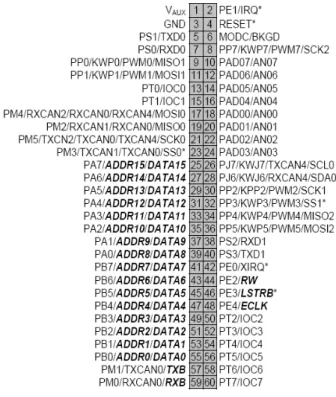
Figure 1 shows the pin-out of the CSMB12C128 module’s 60-pin IDE connector. This pin-out diagram also indicates where on the adjacent IDE socket connector J6 you can access the CSMB12C128 pins, since J5 and J6 are connected “in parallel” with each other, with Pin 1 connected to Pin 1, Pin 2 to Pin 2, etc. Figure 1 must be referred to throughout all of the labs in this course, as it shows how to connect to the various I/O (input/output) pins necessary to interface to external input/output devices.
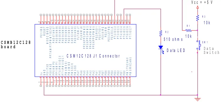
Figure 2 shows an ORCAD schematic diagram that indicates how the CSMB12C128 module might be connected to a switch and an LED. This is the circuit that we used in previous years in this lab, since we had to use the microcontroller module in “stand-alone” fashion, without plugging into the more expensive project board, which was not yet available. Note from Fig. 2 how the pushbutton switch is connected in the pull-down path, and a pull-up resistor (R3) is used to pull the switch output high when the switch is open. The series resistor R1 is used to protect the microcontroller if PT2 is inadvertently programmed as an output, and this output is driven low while the switch button is depressed. Note that when the switch is pushed, the output (connected to input pin PT2) will change from high to low. This is a very standard method of connecting input switches to digital systems which we will follow throughout this course. Also, note how the LEDs are connected in series with a current-limiting resistor. Note that the LED current is limited by the 510 ohm current limiting resistor (R2) to (5-1.4)/510 = 7.1 mA, assuming a forward LED voltage drop of 1.4 V. This resistor protects the LED against burnout, since the LED’s maximum allowable forward current is typically 10 mA. This resistor also protects the microcontroller’s output port pin (PT5), whose maximum driving current should be limited to plus or minus 20 mA. Obviously, it is very important that you always connect LEDs to an output port in series with a suitable current limiting resistor, in order to avoid burning out an output pin on your CSMB12C128 module. Once a pin is burned out, there is no way to fix it; the entire module must be replaced, or at least that pin cannot be used in later work!
C S M 1 2 C 1 2 8 J 1 C o n n e c t o r
1 2 3 4 5 6 7 8 9 10 1 1 1 2
13 15 17 19 21 23 25 27 29
3 0 3 1 3 2 28 2 6 24 2 2 20 18 1 6 14
33 35 37 39 34 36 38 40
4
1 43 45 47 49 51 53 55 57
4
2 44 46 48 50 52 54 56 58
5 9 6 0 V x P E 1/ IR Q G N D R E S E T P S 1/ T X D M O D C /B K G D P S 0/ R X D P P 7/ K W P 7/ P W M 7/ S C K 2 P P 0/ K W P 0 P A D 07 /A N 0 7 P P 1/ K W P 1 P A D 06 /A N 06 P T 0/ P W 0/ IO C 0 P T 1/ P W 0 /I O C 1 P M 4/ M O S I P M 2/ M IS O P M 5/ S C K P M 3/ S S P A 7 P A 6 P A 5 P P 2/ K P P 2 /P W M 2 P A 4 P P 3/ K P P 3 /P W M 3 P J6 /K W J6 P J 7/ K W J7 P A D 03 /A N 0 3 O A D 02 /A N 02 P A D 01 /A N 01 P A D 00 /A N 00 P A D 04 /A N 04 P A D 05 /A N 0 5 P A 3 P A 2 P A 1 P A 0 P P 4/ K P P 4/ P W M 4 P P 5/ K P P 5 /P W M 5 P S 2/ R X D 1 P S 3/ T X D 1 P B 7 P B 6 P B 5 P B 4 P B 3 P B 2 P B 1 P B 0 P M 1/ T X C A N 0 P E 0/ X IR Q P E 2/ R W P E 3/ L S T R B P E 4/ E C L K P T 2/ IO C 2 P T 3/ IO C 3 P T 4/ IO C 4 P T 5/ IO C 5 P T 6/ IO C 6 P M 0/ R X C A N 0 P T 7/ IO C 7 R 2
5 1 0 o h m s
V c c = + 5 V
D a t a L E D
S W 1
C S M B 1 2 C 1 2 8 b o a r d
R 3
1 0 k
D a t a S w i t c h
R 1
1 0 k
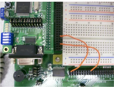
Figure 3. Photograph of the CSMB12C128 plugged into connector J5 of the Project Board, with Pin 1 of the module and Pin 1 of connector J5 aligned. Note how the I/O pins are accessed via connector J6, which is wired in parallel with J5. PT5 (CSMB12C128 Pin 56) is connected to LED1 on the project board, and I/O Port PT2 (CSMB12C128 Pin 50) is connected to pushbutton PB1 on the project board.
Thanks to a generous donation from FreeScale, we now have the project board, which eliminates the need to build the 5 V dc power supply circuit that is shown in Fig. 2. In addition, a number switch circuits similar to the one represented by R1, R3, and SW1 in Fig. 2, as well as several LED circuits similar to the one represented by LED1 and R2 in Fig. 2 have been prebuilt into the project board, so all you need to do is use a single wire to connect the Project Board’s switches and LEDs to whatever I/O pins of the microcontroller that you desire.
Once you have ensured that all jumpers have been properly set on both the module and the project board, and you have plugged the module into the project board as shown in Fig. 0 and Fig. 3, as you were directed to do in the “FreeScale Getting Started” document referred to above, you should now connect pushbutton switch PB1 to I/O pin PB1 and LED1 to I/O pin PB1. From the PBMUSCLK project board schematic diagram (PBMCUSCHEMSLKREVB.pdf) you will see that the switch pull-up resistors and the LED current limiting resistors have already been installed on the project board, so you need not be concerned with connecting these on the project breadboard, but if you were building the circuit without the project board, connecting these resistors would be ESSENTIAL!
Note from the project board schematic diagram that LED buffering through a tristate driver IC is provided to reduce loading on the microcontroller pins. Also the pushbuttons have a 1 kΩ pulldown resistor in series with the pushbutton switch as well as a 10 kΩ pullup resistor. This extra resistor has been added to protect the microcontroller in case a pushbutton switch is inadvertently connected to a microcontroller output pin, so that a direct short to ground will not occur when the pushbutton is depressed. Note that Fig. 2 offered a slightly different solution to the same problem.
6
Our first assembly language example: A computer-controlled flashlight
important, though somewhat trivial, first embedded design example as a “computer controlled flashlight”! We will use the hardware configuration that we just wired: pushbutton switch PB1 is connected to PT2 and LED1 is connected to PT5.
6.1 Use of CodeWarrior IDE to assemble the flashlight program
Section 6 (this section) will list the steps by which the CodeWarrior integrated development environment (IDE) can be used to assemble, download, and debug the software that will control this hardware to make it act as a flashlight. Section 7 explains how a program can be debugged using a simulator, without the use of the physical CSMB12C128 module. Section 8 explains how the program can be
programmed into the flash ROM of the 9S12C128 microcontroller on the CSMB12C128 module and debugged on the actual hardware; this is called “in-circuit debugging”. Fortunately, both the simulator and the in-circuit debugging methods will use the CodeWarrior debugger commands in the same way.
6.1.1 Launch CodeWarrior IDE.
Launch CodeWarrior IDE from Start->All Programs->Freescale CodeWarrior.
If you cannot find this program in your list of programs (perhaps it was installed in Windows 7 localmgr mode, and now you are running in user mode), then browse to C:\
Program Files\Freescale\CodeWarrior for S12(X) V5.0\bin\IDE.exe. You can
drag this program out to your desktop as a “shortcut”, and then clicking on this shortcut will start the CodeWarrior IDE
6.1.2 Create New Project
1. Create a new project by clicking on the “Create New Project” button. 2. A Wizard Map Device and Connection window should appear. Select the
microcontroller derivative you would like to use. Expand the HCS12 category, and then expand the HCS12C family. Click on the MC9S12C128
microcontroller. Also on this page, select the following default connection: Full
Chip Simulation. This tells CodeWarror to simulate the MC9S12C128
microcontroller to permit program debugging; there will be no physical
connection to a microcontroller. Later, the project will be rebuilt and the P&E
Multilink/Cyclone Pro will be specified in order to permit downloading the
code to the physical microcontroller board. The P&E Multilink specifies the type of background debug mode (BDM) interface that is used to download the program via a USB cable and to convey debug information between
CodeWarrior (that runs on your laptop PC) and the microcontroller. Click Next. 3. A Wizard Map Project Parameters window appears. Choose the language to be
used. Uncheck “C” and then check “Absolute Assembly”. Click the Set button to browse to the desired project folder, or to create a new folder. Enter a suitable project name (keep the .mcp project file extension). In the dialog box for Project Name, type LAB1_FLASHLIGHT, click on the Set button to select the desired directory where your project will reside, and then select OK.
Note: there must be NO EMBEDDED SPACES anywhere in the path or the filename.
6.1.3 Entering the flashlight assembly source program
Note the project file name appears near the upper left corner of the screen, just below the toolbar. Just below this is the “project view” that lists the files in the project. Expand the “Sources” category (which contains the source code files) by single-left clicking on the [+}, and then double-left click on the only source code file,
“main.asm”. This should open up a source code editing window labelled main.asm.
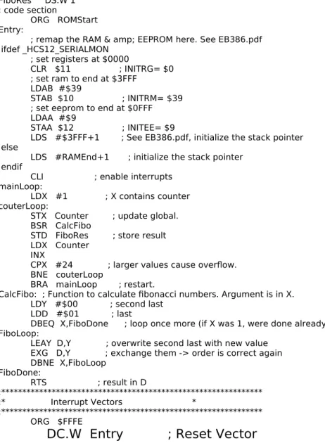
Expand this window so it fills the screen. The initial “main.asm” program serves as a starting template (or “project stationary”, using the CodeWarrior terminology) for the creation of a “single-file, absolute assembly” program. The initial source code template file “main.asm” is shown in Figure 4.
The “memory map” of the CSMB12C128 processor is presented in Table 1. This memory map for our specific processor must be considered when you are customizing the “main.asm” template. Note that an example program variable “tempbyte” (RAM locations that temporarily store data in a program) is allocated by the “Define Space” ds.b directive at the RAMStart location, $0400. The user’s assembly code begins at symbolic location “Entry”, which is made to start at the beginning of the microcontroller’s flash ROM via the “ORG ROMStart” directive. Note that ROMStart
has been set to $4000 using the “EQU” directive, which is indeed correct for our processor.
Table 1: Memory Map (RAM is mapped between 0x400 to 0xFFF via RAM Position Register)
The
microcontroller’s RESET vector consists of the final two bytes of memory space,
$FFFE and $FFFF. Upon system reset (upon pressing the RESET button or upon
power-up) the processor loads its 16-bit “program counter” with the two bytes found at locations $FFFE and $FFFF, and thus it begins executing the code starting at the address contained in these two locations, where $FFFE contains the high byte of the address, and $FFFE contains the low byte of the address. Normally, these two
locations are loaded with the high and low bytes (respectively) of the starting address of the user program, which is symbolically tagged by the symbol “Entry” in the
main.asm template. In fact, this is what the main.asm template file has done in the
$FFFF. The high byte of the program starting address is placed at address $FFFE and the low byte of the program starting address is placed at address $FF
; export symbols
XDEF Entry ; export 'Entry' symbol
ABSENTRY Entry ; for absolute assembly: mark this as application entry point ; include derivative specific macros
INCLUDE 'mc9S12C128.inc'
ROMStart EQU $4000 ; absolute address to place my code/constant data ; variable/data section
ifdef _HCS12_SERIALMON
ORG $3FFF - (RAMEnd - RAMStart) ; Since we have a 2 kbyte RAM block, ;this = $3800.
else
ORG RAMStart ;RAMStart is defined in the mc9S12C128.inc ;file to = 0x0400.
endif
; Insert here your data definition. Counter DS.W 1
FiboRes DS.W 1 ; code section
ORG ROMStart Entry:
; remap the RAM & amp; EEPROM here. See EB386.pdf ifdef _HCS12_SERIALMON
; set registers at $0000
CLR $11 ; INITRG= $0 ; set ram to end at $3FFF
LDAB #$39
STAB $10 ; INITRM= $39 ; set eeprom to end at $0FFF LDAA #$9
STAA $12 ; INITEE= $9
LDS #$3FFF+1 ; See EB386.pdf, initialize the stack pointer else
LDS #RAMEnd+1 ; initialize the stack pointer endif
CLI ; enable interrupts mainLoop:
LDX #1 ; X contains counter couterLoop:
STX Counter ; update global. BSR CalcFibo
STD FiboRes ; store result LDX Counter
INX
CPX #24 ; larger values cause overflow. BNE couterLoop
BRA mainLoop ; restart.
CalcFibo: ; Function to calculate fibonacci numbers. Argument is in X. LDY #$00 ; second last
LDD #$01 ; last
DBEQ X,FiboDone ; loop once more (if X was 1, were done already) FiboLoop:
LEAY D,Y ; overwrite second last with new value EXG D,Y ; exchange them -> order is correct again DBNE X,FiboLoop
FiboDone:
RTS ; result in D
;************************************************************** ;* Interrupt Vectors *
;************************************************************** ORG $FFFE
DC.W Entry ; Reset Vector
To turn the template file of Figure 4 into the flashlight program, please modify this
main.asm template file so that it now looks like Figure 5. (This can be done by
cutting and pasting the flashlight program code from the Lab 1 folder that you downloaded from Angel.)
***************************************************************************** * Flashlight Program For CSMB12C128 module
* PT5 configured as output pin to drive an LED, and PT2 configured as a * digital input, connected to a pushbutton switch.
* Lines of code that start with an asterisk or a semicolon are comment lines. **********************************************************************************
XDEF Flashlight_Entry ; export 'Flashlight_Entry' symbol
ABSENTRY Flashlight_Entry ; for absolute assembly: mark this as pgm entry
point
RAMStart EQU $0400 ; absolute address to place my variables
ROMStart EQU $4000 ; absolute address to place my code/constant data DDRT EQU $242 ; Data Direction Reg for PORT T
PTT EQU $240 ; Data Reg for PORT T
ORG ROMStart ;Start assembling program at location $4000
Flashlight_Entry:
BCLR DDRT,%00000100 ;bit clear will clear bit 2 to make PT2 a switch input BSET DDRT,%00100000 ;bit set will set bit 5 to make PT5 an output to drive LED AGAIN:
LDAA PTT ;load port T value into accumulator A. Pin PT2 is the pushbutton
switch
ROLA
;rotate accumulator A with carry one bit to right so that Bit 3 of accumulator
;A holds state of switch.
ROLA ;Now Bit 4 of accumulator A holds state of switch
ROLA ;Now Bit 5 of accumulator A holds state of switch
;Store accumulator A contents out to Port T so that the switch state is shown
;on LED connected to PT5 STAA PTT
BRA AGAIN ;Loop back to get new state of switch.
ORG $FFFE ;Assemble next byte into location $FFFE, which is Reset Vector location
DC.W Flashlight_Entry ;The DC.W (or FDB) directive allocates two bytes
;and stores the value “Flashlight_Entry” at Reset Vector ;location as starting address when reset
Figure 5. The flashlight program source code.
6.1.4 Building the project
Once the main.asm file has been modified according to Figure 5, click on the “Make” icon (6th icon from the right along the top of the CodeWarrior main window. If
assembly errors are encountered, you can click on the indicated error message to take you to the erroneous line in the text editor in order to fix it. Eventually the program should assemble without error.
therefore it cannot be examined with a text editor. It contains the executable (binary) machine code as well as some additional debug information. In addition, a similar file with an “.abs.s19” file extension is also generated. This (larger) file is holds the same binary machine code data in a printable “ASCII text” “S-record” format that Motorola (now FreeScale) has long used for downloading code from a host PC to a target microcontroller. A printout of this S-record file appears as follows.
6.1.5 Motorola S-Record Absolute (ASCII Text) Machine Code File Format
Each line of text in the S-Record represents a different “S-record”. The first two characters in each line indicate the record type. The first line will always contain an “S0” record, which holds debugging information, followed by one or more “S1” (assembled machine code) record lines, and the last line always contains an “S9” (terminating) record. The next two characters on each line convey the number (in hexadecimal) of the remaining bytes in the record line. Each pair of characters that follows constitutes a pair of ASCII characters that indicates a byte of data expressed in hexadecimal. Therefore, each of these ASCII characters that follow can only take on the ASCII codes for the digits 0 – 9 and the letters A – F. The last pair of characters on each line is an ASCII-encoded hexadecimal checksum byte that is formed by adding the previous characters on the line in a special, prescribed fashion. This “redundant” error checking value can be recalculated by the microcontroller software by adding the received characters as it downloads each line of the S-record file. The calculated checksum value for each line can be compared with the received checksum value, in order to verify the integrity of the data received in each line.
The first line is always an “S0” record, which contains ASCII text information that contains debugging information, but no actual assembled machine code. The S0 record shown in the first line of the example above indicates that this record is $84 bytes long (remember each byte is a pair of characters). Because the S0 record in this example was quite long, I had to truncate it. Using an ASCII table, one can determine that the ASCII text that follows the byte count is: “3:\Documents and Settings\
Administrator\….”. (Evidently, this S0 record begins with the file directory path to the project folder for this program!)
Following the “S0” record line comes one or more “S1” record lines (in this case there are two) that contain the assembled machine code and initialized data. In the second line of the S-Record we see that the first byte following the “S1” characters is $22. This tells us that this first S1 record is $22 = 34 bytes long. The next two bytes (4 characters) in this record indicate the address ($4000) of the first data byte to be allocated. Next come the machine code bytes. In this case, we see that $10 is to be loaded into address $4000, $EF into address $4001, $18 into address $4002, etc. Note that this makes sense, since the first executable instruction in our source program was “CLI” (clear interrupt mask flag), and its 2-byte OPCODE (according to Appendix A of our textbook) is $10EF. This process continues up to where $11 is
S04F0000433A5C446F63756D656E747320616E642053657474696E67735C6C6F6361 6C6D67725C4465736B746F705C6C6162315C62696E5C48435331325F53657269616C 5F4D6F6E69746F722E61627326
S11740001D0242041C024280B60240464646467A024020F483 S105FFFE4000BD
loaded into $401E, which is the last byte of code in the program. Recall that the final byte on the line ($15) is NOT a byte of machine code, but rather it is the checksum for that record.
In the third line of the S-Record we find a second S1 record. This one is initializes the reset vector by loading $4000 into locations $FFFE and $FFFF, and it is a result of the last two lines (excluding comment lines) in the assembly source file. The last line is always an “S9” record, which merely indicates the end of the S-record file.
6.1.6 Assembly Listing File
It may be helpful during program debugging to see the assembled machine code, as well as the data allocations, that the assembler made during the assembly process placed beside each corresponding line of assembly code of the source assembly program (main.asm). This is easily done inside the CodeWarrior IDE by clicking on Project – Disassemble. A new window displaying the assembly listing file
“main.asm.o..lst” will appear, as shown in Figure 6.
Freescale HC12-Assembler (c) Copyright Freescale 1987-2006
Abs. Rel. Loc Obj. code Source line ---- ---- --- ---
1 1 ********************************************************************************* 2 2 * Flashlight Program For CSMB12C128 module
3 3 * PT5 configured as output pin to drive an LED, and PT2 configured as a 4 4 * digital input, connected to a pushbutton switch.
5 5 * Lines of code that start with an asterisk or a semicolon are comment lines. 6 6 ********************************************************************************** 7 7 ; export symbols
8 8 XDEF Flashlight_Entry ; export 'Flashlight_Entry' symbol
9 9 ABSENTRY Flashlight_Entry ; for absolute assembly: mark this as pgm entry point 10 10 ;symbolic definitions
11 11 0000 0400 RAMStart EQU $0400 ; absolute address to place my variables
12 12 0000 4000 ROMStart EQU $4000 ; absolute address to place my code/constant data 13 13 0000 0242 DDRT EQU $242 ; Data Direction Reg for PORT T
14 14 0000 0240 PTT EQU $240 ; Data Reg for PORT T 15 15
16 16 ; code section
17 17 ORG ROMStart ;Start assembling program at location $4000 18 18 Flashlight_Entry:
19 19 a004000 1D02 4204 BCLR DDRT,%00000100 ;bit clear will clear bit 2 to make PT2 a switch input 20 20 a004004 1C02 4220 BSET DDRT,%00100000 ;bit set will set bit 5 to make PT5 an output TO drive LED
21 21 AGAIN:
22 22 a004008 B602 40 LDAA PTT ;load port T value into accumulator A. Pin PT2 is the pushbutton switch 23 23 a00400B 45 ROLA
24 24 ;rotate accumulator A with carry one bit to right so that Bit 3 of accumulator A holds state of switch.
25 25 a00400C 45 ROLA ;Now Bit 4 of accumulator A holds state of switch 26 26 a00400D 45 ROLA ;Now Bit 5 of accumulator A holds state of switch
27 27 ;Store accumulator A contents out to Port T so that the switch state is shown on LED connected to PT5
28 28 a00400E 7A02 40 STAA PTT
29 29 a004011 20F5 BRA AGAIN ;Loop back to get new state of switch. 30 30
31 31 ORG $FFFE ;Assemble next byte into location $FFFE, which is Reset Vector location 32 32 a00FFFE 4000 DC.W Flashlight_Entry ; DC.W (or FDB) directive allocates two bytes
Figure 6. Assembly listing file “main.asm.o.lst” that shows the assembled machine code for the flashlight program and also the address of each machine instruction.
7
CodeWarrior Simulator: program debugging without the CSMB12C128 module
The CodeWarrior simulator allows you to simulate program execution, and thereby verify proper operation of your program, on your PC, even when the actual
CSMB12C128 hardware module is not connected to your PC! Such debugging should be limited to non-I/O intensive programs, however, since the simulator does not have access to the actual hardware. Simple switch/LED I/O can be simulated by modifying register contents and watching selected register locations. Further details about the use of this simulator can be found in the “Manual True Time Simulator HC12.pdf” document included in the AFS class folder.
In the upper left CodeWarrior IDE selection box that is labeled
“lab1_flashlight.mcp”, select the “Full Chip Simulation” option. Click on the
green “Debug” icon. The True-Time simulator window appears. Click on the “Reset Target” button at the top of the simulator window (first button on the right), or type <Ctrl-R>. The first instruction in the source window (where the source program is displayed) should be highlighted, indicating that the program has been reset to its starting point. At any time in the debugging process you want to start the program back at its beginning, press this button.
Right-click somewhere inside the Memory Window, choose Format, and select
Binary. The memory window now displays its contents in binary. Again right-click
inside the Memory Window, choose Address, and enter 240. Now the Memory
Window displays memory addresses starting at hex 240. We are interested in the
binary contents of address hex 240 (PTT) and hex 242 (DDRT).
Click the “Single Step” button (2nd button from right), or type <F11>. You will
see the program take a step. Press the Single Step button several more times, and watch the Register Window, to ascertain that the microcontroller’s registers are changing as expected. Watch the memory window, at address hex 242 to see that the DDRT is properly configured so that PT5 = 1 (output) and PT2 = 0 (input) after the BSET and the BCLR instructions have executed. After you step past the LDAA PTT instruction, note the value of Bit #2 in PTT (hex 240). This represents the PT2 bit. We can simulate the state of the switch on PT2 by modifying Accumulator A just after the LDAA PTT has executed. Go to the Register Window, and select (highlight)
Accumulator A with your mouse. Then type in a new value with bit position #2 set either high or low (to indicate the intended state of the switch), that is, enter either 00 or 04. Be sure to hit the Enter key to ensure that this new value has been written to Accumulator A before resuming single stepping.
Continue single stepping until the program branches back to the top of the loop. Notice that PT5 should change to the desired value of PT2 just after the STAA PTT instruction executes. Note that when a register changes its contents in the memory window, it is highlighted in red.
hit, we can continue single-stepping from there. To see how this is done, right click on the first ROL A instruction in the Source window of the debugger. Then select the “Set Breakpoint” option. A red arrow will be displayed to the left of this instruction, indicating that a breakpoint has been set there.
Now click the “Reset Target” button to start the program at its beginning, and next hit the green simulation Run button (7th button from the right). The program will
run at speed until the breakpoint is hit, as evidenced by the highlighting of the
breakpointed instruction. Once the breakpoint is hit, set Accumulator A to the desired value (either a 00 or a 04, and then try single stepping from this point (by hitting the
Single-Step button). Also, try experimenting with setting several simultaneous
breakpoints in the code, and then running between them by successive depressions of the Run button.
Breakpoints may be removed by right clicking on a line in the Source window
where a breakpoint was previously set and selecting the Delete Breakpoint option. With single-stepping and breakpoint setting, along with judicious examination of the
Register, Memory, and Data windows, the programmer has no excuse for not
being able to debug an assembly language program!
8
Using the CodeWarrior In-Circuit Background Debugger (BDM)
In this section we shall learn how to use the CodeWarrior background debugging mode (BDM) USB cable debugger to download our program from the PC into the CSMB12C128’s flash memory. We shall then learn how to use the debugger
(fortunately, it is the same one we learned about in the previous simulator section!), which will allow us to debug and run the code on the actual target hardware. Using the actual hardware is usually preferable to using the simulator to debug an
embedded control program. However, the simulator is more convenient when you do not have ready access to the hardware, or when the hardware does not yet exist.
8.1 Preparation before launching the BDM debugger
Before you start the CodeWarrior debugger, first check the following: (1) Make sure the CSMB12C128 module is properly plugged into J5 on the PBMUSCLK project board. (2) Plug in the USB cable you’re your laptop PC to the project board. Make sure that the CSMB12C128 module’s green Vdd (+5 V dc power) LED is lit, to ensure it is getting dc power from the project board.
8.2 Using the CodeWarrior IDE with the BDM debug monitor
If necessary, close the simulator debugger window (which may be still open from the last section) by hitting “X” in the upper right corner of this window. Then select the box just under the “lab1_flashlight.mcp” label on the left side of the screen. Change this box from “Full Chip Simulator” to . “P&E Multilink CyclonePro”. From the IDE window, make sure the “main.asm” file is highlighted in the left window, click the “Compile” button (7 buttons from the right) and the “Make” icon (6 buttons from the right), to ensure that the project files are up to date. Click on the green
Debug icon (4th from the right). If you get a message that warns you that the flash
8.3 Debugging with the in-circuit debugger
Just as you did in the simulator debugging section above (Section 7), you may once again use this debugging window to step through the program using the
“Single-Step” icon. The only difference is that now the “LDAA PTT” instruction will load into the accumulator A the actual state of the physical switch that is connected on your breadboard! (Try stepping around the program loop with the switch both pressed and not pressed to verify this is true!) Also, the “STAA PTT” instruction will actually transfer data out to the physical LED on your board. Be sure to also watch the contents of the PTT data port register (at address $240) as you step around the
program loop. Note that when the LDAA PTT instruction executes, the LSB of PTT which follows the state of the input switch on your breadboard, is transferred to
Accumulator A. When STAA PTT executes, the MSB of the Accumulator A is transferred to the MSB of PTT, which sets the logic state of the LED on your breadboard.
You may also set breakpoints, as before. First you will need to reset the program. If you press the debugger window’s “reset target” button to reset the program counter to point to the first instruction in the program.
Now try setting a breakpoint as you did before at some intermediate instruction. Once you run at speed (by pressing the green arrow “Start/Continue” icon) to the breakpoint, you may begin single-stepping from there, or you may press the green run arrow and run at speed until the next breakpoint is encountered. Try experimenting with setting multiple breakpoints in your code.
Now remove all breakpoints and run the program by clicking on the green Run button. Note that the physical LED will turn off whenever the switch is depressed. You need to click Halt to stop execution. Note that the instruction that was executed just before the Halt button was pressed is highlighted. You can then press the Reset Target button to reset the program counter to point to the first instruction in the program.
8.4 Stand-alone execution of the user program
After halting the program execution (by pressing the Halt icon) and exiting from the debugger, you can hit the RESET button on your CSMB12C128 module. You will find that the flashlight user program should begin executing immediately! The fully-debugged user application is now running independently of the BDM debugger. In fact, if you were powering the project board using its external dc power module, you could even unplug the USB cable between the laptop PC and the project board, and the program would continue to run. Even if you turn off the power to the CSMB12C128 and then turn it on later, you could press the RESET button on the CSMB12C128
module and start running the program, since it has been programmed into the CSMB12C128’s non-volatile flash memory, which does not lose data even when the power is turned off.
9
Second assembly language example: Coin-Tossing Program
Now let us consider a more interesting (and more complex) embedded design assembly language example.
9.1 Coin-Tossing Program Specification
In this second embedded design example of a coin tosser, the hardware
configuration has been changes so that the pushbutton switch is moved to Pin #1 of Port B (PB1), and the LED is moved to Pin #0 of Port B (PB0). Every “click” of the pushbutton (by “click”, I mean pressing the pushbutton switch down, and then releasing it), will simulate a single toss of a coin, with the LED state coming up in a random state, where LED = ON implies a “Heads” outcome, and LED = OFF implies a “Tails” outcome. The LED stays in this state until the next click. In addition, statistics indicating the outcomes are displayed on the 8-bit I/O ports PORT T (PTT) and PORT AD (PTAD). The total number of “Heads” outcomes is accumulated, as an 8-bit binary number, on Port AD; and the total number of “Tails” outcomes is accumulated on Port T. (We will not bother to actually wire 8 LEDs to Port T and 8 LEDs Port AD to display these statistics, as this would be quite tedious; instead we will move a logic probe or scope probe along these 16 pins to observe that the proper number of Heads and Tails outcomes is being displayed as the pushbutton is successively clicked.)
9.2 Charting your course: the program flowchart
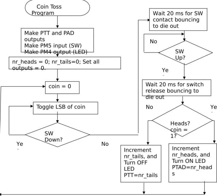
After the product specification is compete, the programmer must construct a hardware block diagram that shows the hardware that must be controlled, and then construct a program flowchart that indicates, at a high level, what the program must do to properly control the hardware.
A flowchart is a high-level description of the structure of a program. A flowchart consists of just four components: an oval starting block, that indicates the name of the program; rectangular processing blocks, which indicate major processing steps that must be performed in the program; diamond shape decision (conditional
branching) boxes, that decide which processing step is to be performed next based
upon the data being processed by the program; and the interconnecting flow
direction arrow lines.
Just like an outline for a term paper, the flowchart is used to chart the course that the programmer plans to take in order to implement the program. And just like with a term paper outline, the flow chart should be constructed first, not last in the software design process! Once the program flowchart has been constructed, the interesting, creative software design work has been accomplished! All that remains is for the programmer to fill in the low-level details by actually coding the program.
However, human nature often runs counter to the idea of flowcharting (or term paper outlining). We humans tend to be impatient and impulsive. We are anxious to jump in and start programming without doing the requisite high-level planning
(flowcharting) first! But consider how a traveller who takes the time to plan and map out their trip before leaving on it usually has a straighter, cleaner journey toward their goal, and does not get lost as often. The flowchart helps the programmer march more directly, efficiently, and cleanly toward the goal!
In an embedded design, the flowchart must be accompanied by a hardware block diagram, or in a simple case, a complete schematic diagram such as that shown in Figure 2, which shows the hardware devices that the program must interact with, and indicates their corresponding signal names that are referred to in the flowchart. In fact, the hardware diagram must be constructed before the flowchart, since you have to know exactly what hardware you are going to control before you can write the program to control it!
forest for the trees” if you try to understand a large program by looking directly at its code (especially if it is assembly code).
Figure 7. Example flowchart for a “coin-tossing” program (Drafted using the “Flowchart” Auto Shape Symbols in MSWORD found by clicking on Insert – Picture – Autoshapes)
One must decide on the appropriate “complexity level” of the flowchart. A flowchart is at too “low of a level” (too detailed) when basically each processing block and decision diamond in the flow chart represents what is done by just one machine instruction in the program. On the other hand, a flow chart that consists of just three processing blocks labelled: “Get data from input switches”, “Calculate result from input data” and “Output result to LEDs” would be too high a level, since the flowchart does not give enough information about how the result is calculated to be very useful! There has to be a happy medium in a flowchart, where enough of the detail is
Coin Toss
Program
Make PTT and PAD
outputs
Make PM5 input (SW)
Make PM4 output (LED)
nr_heads = 0; nr_tails=0; Set all
outputs = 0.
coin = 0
Toggle LSB of coin
SW
Down?
Ye
s
Wait 20 ms for SW
contact bouncing
to die out
SW
Up?
Ye
s
No
No
Wait 20 ms for switch
release bouncing to
die out
Heads?
coin =
1?
Ye
s
No
Increment
nr_tails, and
Turn OFF
LED
PTT=nr_tails
presented so that the programmer can easily write the program from the flowchart, but at the same time not overwhelm the reader with too much detail.
The flowchart of Figure 7 indicates the logical flow and structure of the coin-tosser program of Figure 8. First the data direction registers and the PORTAD digital I/O enable register are set up so that all eight bits of PORT AD and PORT T are configured as digital outputs and PORT B has Bit #1 (PB1) configured as a digital input (for the pushbutton switch) and PORT B has Bit #0 (PB0) configured as a digital output (for the Head/Tails LED). The nr_heads and nr_tails variables (memory locations), which will accumulate the total number of heads and tails outcomes, are initialized to zero.
;***************************************************************************** ;* Coin Tosser Program Example (KEH) 8/5/2008 for the CSMB12C128 Module ;* Pushbutton SW on PB1, LED on PB0, PTAD holds nr. Heads, PTT holds nr. Tails ;***************************************************************************** ; export symbols
XDEF cointoss ; export 'Entry' symbol
ABSENTRY cointoss ; for absolute assembly: mark this as application
entry point
nolist
INCLUDE 'mc9s12c128.inc' ; This include file has all the 9S12C128
register EQU's in it!
list
PushButton: equ PORTB
LEDDisplay: equ PORTB
ShowNumberOfHeads: equ PTAD
ShowNumberOfTails: equ PTT
; variable/data section ORG RAMStart
nr_heads: ds.b 1 ;Allocate 1 byte of RAM: Number of head outcomes
accumulated here
nr_tails: ds.b 1 ;Allocate 1 byte of RAM: Number of tail outcomes
accumulated here ; code section
ORG ROM_4000Start ;This is the symbol for the ROM start address in the 'mc9s12c128.inc' file.
cointoss:
lds #RAMEnd ; Initialize stack pointer to top of RAM
bset DDRAD,$FF ; Port AD will be output port to display (as an 8-bit binary nr) the nr of
heads.
bset DDRT,$FF ; Port T is will be output port to display (as an 8-bit binary nr) the
nr of tails.
bset DDRB,%00000001 ; PB0 is "Head/Tail" LED output.
bclr DDRB,%00000010 ; PB1 is pushbutton "die toss" switch input.
clr nr_heads ; Initialize statistics to 0.
clr nr_tails
clr ShowNumberOfTails ; Zero the number of tails displayed on Port T
clr LEDDisplay ; Turn off the heads/tails LED
clr ShowNumberOfHeads ; Zero the number of heads displayed on Port AD
Top_of_loop:
clrb ; Use B as a 1-bit counter that will be stopped when the switch is
depressed and
;thereby will contain a random outcome: either 0 or 1.
SW_wt_press:
ldaa PushButton ; Load accum A with the SW state (Only Bit #1 matters)
anda #$02 ; Accum A = $02 if SW not pressed, and $00 if SW pressed
bne SW_wt_press ; Hang in this loop until SW is pressed
jsr delay_rtn ; Wait for pushbutton switch to stop bouncing
SW_wt_release:
ldaa PushButton ; Arrive here when SW is pressed, with random outcome in Accum B
anda #$02
beq SW_wt_release ; Hang in this loop until switch is released.
jsr delay_rtn ; Wait for pushbutton switch to stop bouncing by calling delay_rtn
subroutine.
stab LEDDisplay ; Send HEAD/TAIL result to LED on Bit 0 of PORTB.
cmpb #1 ; If HEAD outcome, B = 1. If TAIL outcome, B = 0.
beq heads_outcome tails_outcome:
inc nr_tails ; Update nr_tails RAM location
movb nr_tails,ShowNumberOfTails ; Mirror this value on Port T
bra Top_of_loop heads_outcome:
inc nr_heads ; Update nr_heads RAM location
movb nr_heads,ShowNumberOfHeads ; Mirror this on Port AD bra Top_of_loop
;*********** End of main program******************* ; Here is a short delay subroutine that delays for about
; 20 ms before returning. It is used for pushbutton switch debouncing delay_rtn:
ldy #$ffff delay_more:
dey ;
bne delay_more ;Count y down from $ffff to 0.
rts ;Return addr (pop return addr off stack into PC)
; Here we intialize the RESET vector to point to the ; start of the cointoss program
ORG $FFFE
dcw cointoss ; Intialize Reset Vector with starting address of coin toss program
Figure 8. The Coin Tossing Program.
The program now enters its infinite processing loop. The first step in this
processing loop is a short internal loop (see the lower left of the flowchart) where the least-significant bit (LSB) of accumulator register B, is used to indicate the head/tails outcome. This LSB is toggled (changed) back and forth between 0 and 1 very quickly until the user presses the pushbutton switch, at which time the program execution falls out of this first internal loop. At this point, the LSB of accumulator B contains a random head or tails outcome, since the pushbutton will be pressed at a random time and the LSB is being toggled back and forth very quickly. Next the program waits 20 ms for the switch contact bouncing to die out before the state of the pushbutton switch is again looked at by the program. This is a very important step, since after the contacts of any mechanical switch close, they will bounce (or “chatter”) rapidly
Program execution then enters a second short internal loop (top right of the flowchart), where we wait for the pushbutton switch to be released. Once again, the switch contacts might once again bounce as the contacts of the switch are opened, so we once again must delay 20 ms. In general, any mechanical switch tends to bounce for a few milliseconds both when the switch is pressed (“make”) and when the switch is released (“break”). Next, the LSB of accumulator B is checked for the outcome and either nr_heads or nr_tails is incremented, the result is displayed in the LED, and program execution returns to the top of the infinite processing loop.
9.3 Writing the actual program
Once the flowchart is complete, an assembly-language program that implements the flowchart is easily written (see Figure 8). Make sure that you understand each instruction in this program and how it implements the flowchart of Figure 7.
Note the use of the “INCLUDE mc9S12C128.inc”. This file consists of a large collection of equate (EQU) statements that symbolically define the microcontroller’s register addresses and the contents of these addresses. The INCLUDE statement inserts all of the text inside the mentioned “.inc” file at the position of the INCLUDE statement before the compiler begins compiling the program. Please take the time look over the contents of this file, which can be found at
C:\Program Files\Freescale\CodeWarrior for S12(X) V5.0\lib\hc12c\ include
Or you can view this file by expanding the “Includes” tab in the project view window and then clicking on mc9S12C128.inc.
By including this file at the top of a 9S12C128 assembly program, we can save a lot of typing EQU statements at the top of our program and avoid hard-to-find address assignment errors!
9.4 Making the project and using the BDM debugger
Make a new project with the Project Wizard. When you get to the step where you are to modify the template main.asm file, copy the “main.asm” file in the “Coin Toss Example” folder that may be downloaded from the Lab 1 AFS class folder in the place of the template main.asm file. This “main.asm” file contains the “Coin Tossing
program shown in Figure 8.
Once the project creation is complete, expand the Libraries category in the
“project view” by clicking on the {+} next to it. Then click on the “
mc9s12c128.inc
” file to open it up. Note that this file contains a very long series of equate (EQU)statements that associate each of Freescale’s “official”
mc9s12c128.inc
microcontroller register names with their respective addresses, such as “PTT: EQU $240” and“PORTB: EQU $01”, etc. By including this file, you do not have to define the address
each of the symbolic register addresses as you did in the flashlight program. Likewise, note that the symbol “RAMStart” may be used to specify the starting address of RAM (0x400), and the symbol “ROM_4000Start” may be used to specify the starting address of ROM (0x4000). Note that this file has been included at the beginning of the
Click on the main.asm program in the “Sources” category to open up an editing window. Then click on the “Make” icon to assemble the source program. After you have successfully assembled this program, you should now try running this program with the in-circuit debugger, following the steps outlined in Section 9. Try setting a breakpoint at the “STAB LEDDisplay” (STAB PORTB) instruction. Then, when you run the program, you will not hit this breakpoint until the switch has been “clicked”
(pressed down and then released). From this point you can single-step through the program, noting how the correct variable (nr_heads or nr_tails) gets updated. When you remove the breakpoint, you should be able to observe the proper operation of the program, where a random LED state is displayed after each button click, and a logic probe may be used to observe that the correct number of heads is accumulated on PORT T and the correct number of tails is accumulated on PORT AD.
9.5 Debugging without the CSMB12C128 Hardware: using the Simulator
You might also want to try using the simulator to verify the correct operation of this program, though it is not quite as easy to verify program operation without the actual microcontroller hardware being present. This can be done by following the same kind of steps you followed in Section 8. For example, setting the Memory
Window address to 0 allows you to observe PORTB and DDRB, while setting the
memory address window to hex 240 allows you to observe PTT and DDRT. I recommend setting the format of the displayed memory addresses in the Memory Window to “Binary”.
Now begin single-stepping through the program. Click on the “Step Over” button (5th button from the right), as you single step in this example, so you will step over
(not into) the called delay subroutine. If you step into the delay subroutine, it will take to long to step all the way through it! Another option is to set a breakpoint at the RTS of the delay routine. Then if you step into it, you can hit the Start/Continue button to run through it at full speed until the RTS is hit. Then you can step out of the routine back to where it was called.
When you hit either of the two “LDAA PORTB” instructions, which are used in the program to read the state of the switch on Bit #1 of PORT B, take one more step to the
“ANDA #$01” instruction, and then double left click on Accumulator A in the
Register Window to highlight it. Then type in either a “01” (switch UP) or a “00” (switch down) to simulate the switch being read as either high or low. THEN BE SURE TO HIT “ENTER” BEFORE TAKING ANOTHER STEP, IN ORDER TO ACTUALLY LOAD THIS VALUE INTO ACCUMULATOR A. You may now resume single-stepping. You should be able to simulate several heads and tails outcomes in this way. You should be able to watch the current head or tail outcome get displayed in Bit #0 of Port B (memory window address 1), and also watch the number of heads accumulate on Port AD (memory window address 270), and the number of tails accumulate on the eight bits of PORT T (memory window address 240).
10 Your first embedded design assignment: A “fair” dice tosser!
Your first assembly-language programming assignment is, after completing the previous exercises and thoroughly understanding the flashlight and the coin-tosser programs, to modify the coin-tossing assembly language program of Figure 8 to make it into a (reasonably fair!) six-sided “die-tosser”.
Next, using the coin-tossing example of Fig. 8, as a starting point, write a dice-tossing program so that every time the button is clicked (pressed, then released), a random binary number between 1 and 6 is displayed on the three LEDs. The state of the LEDs should remain stable between each click, holding the previous outcome of the die toss. A new outcome should appear after each click.
In a manner similar to that of the coin tosser example, allocate six RAM data bytes using the “define space” (DS.B) directive to keep track of the number of times the die tosser has come up with each possible outcome (1 – 6). However, these statistics cannot be displayed on I/O pins, since we would run out of I/O ports! (We will learn later several methods for expanding the I/O capability of a microcontroller.) Instead, these statistics can be checked by observing the value of each of these variables in the in-circuit debugger’s “Data window” after program execution has been halted.
Test your dice tosser by operating the pushbutton switch for a minimum of 250 times (1000 times would be even better!), and record the final contents of these RAM locations in your report. (Hopefully you will be able to show that your dice tosser is “fair”, with approximately equal numbers being accumulated for each of the six possible outcomes.)
Demonstrate your working coin tosser program to the lab instructor, getting his signature on your (well-commented!) assembly source file.
Your lab report should be “memo style”, and it must follow the format described in the first day handout. In particular, this first lab report must consist of a memo that specifically refers to the following four attachments (or appendices):
(1) Schematic diagram of your hardware interface circuit. Your schematic should be similar to that drawn for the flashlight example shown in Figure 2. Your hardware schematic must be drafted using ORCAD Lite 9.2, which you can install from the class AFS folder. The symbol for the CSMB12C128 microcontroller module (See Figure 2) can be accessed by opening up the ORCAD schematic that corresponds to Figure 2. This may be found in the class Lab 1 AFS folder in a folder labelled “CSMB12C128 lab1 Orcad schematic”. Open this ORCAD project and cut and paste this circuit into a new schematic in a new project file. You may then modify this circuit (only slightly) to obtain the schematic of your dice tossing project. Many other useful ORCAD symbols can be found in the “Digikey” ORCAD parts library, which may be installed after you finish installing ORCAD Lite 9.2. This parts library is also provided in the class AFS folder.
(2) Flowchart of your die-tossing program, using the flowchart of Fig. 7 as a model.
(3) A well-commented printout of your die-tossing assembly source (*.asm) file,
and also the corresponding assembly listing (*.lst) file that was generated by the
assembly process. This *.lst file shows the work done by the assembler.
Each of these attachments must be numbered and labelled appropriately with a meaningful caption. Each attachment must be referred to and also discussed in the text of your memo. This is an important technical writing rule that I require you to follow in this and in all subsequent lab memos.
11 Possible Errors and Solutions
11.1 Elf Loader Error
Check the following to fix the error by choosing Monitor-HCS12->Load options
11.2 Simulator RAM range error
RAM range in the simulator may not be set correctly. For example, The initial RAM range might be from 0x3800 to 0x3800. It should be changed to 0x3800 to 0x3FFF as follows under Simulator->HCS12FCS>Configure….. This error may cause stack not to work correctly. For example, a
11.3 Error message: L1116: Function main not found
This message will occur when the project does not have a function named “main”. It seems that one function must be named main, which is the starting point of the object code for a project.
11.4 Error in command file .\cmd\monitor_postload.cmd!
The process should be the label to start the main program. Use this in general: Findproc main. Declare main as your reset vector. The following example declares maximum as the starting address of the code.
11.5 Warning on dbg file