Serving the Montium:
Design of an energy-efficient processor-network interface
Marcel D. van de Burgwal s9906738
MSc thesis University of Twente
Department of EEMCS, Embedded Systems
Committee: dr. ir. G.J.M. Smit
ir. E. Molenkamp dr. ir. P.M. Heysters
ir. P.T. Wolkotte N.K. Kavaldjiev
Abstract
English
In this thesis, a description is given of the design and implementation of a communication and configura-tion unit (CCU). The CCU is part of the Chameleon architecture, a tile based system on chip consisting of several tiles and a network on chip. The CCU serves as an hardware interface between the network
and a tile. Starting at the highest level (using a black box view), a protocol is designed. The protocol contains some standard functions such as read, write, execute and stop and a few specific functions. Subsequently, the internal architecture is clarified block-by-block. A hardware realization is discussed
and it is shown that the results meet requirements. Furthermore, a number of applications are presented, which provide relevant insight and information on the possibilities and performance of the CCU. Several
communication models are used to calculate the minimal theoretical clock frequencies needed to make sure no data loss occurs. Finally, we give a number of recommendations and the thesis is completed with
the conclusion that the implementation of the CCU fullfills its requirements.
Nederlands
Dit doctoraalverslag beschrijft het ontwerp en implementatie van een communicatie en configuratie unit (CCU). De CCU is ontwikkeld voor de Chameleon architectuur, een architectuur voor chips bestaand uit
kleine tegels (tiles) die met elkaar kunnen communiceren via een netwerk (network on chip). De CCU dient hierbij als de netwerk interface voor een tegel. De tegels kunnen worden bestuurd door middel van commando’s die door de CCU worden afgehandeld. Door een tegel als een black-box te beschouwen,
hebben we een berichten protocol opgesteld dat naast de veel voorkomende functies als lees-, schrijf-en configuratieacties ook specifieke functies als startschrijf-en, stoppschrijf-en schrijf-en resettschrijf-en bevat. Door deze berichtschrijf-en
te combineren met gestelde randvoorwaarden is het mogelijk om een hardware ontwerp te maken. Dit ontwerp is volledig gebaseerd op de functionaliteit die het communicatie protocol ondersteunt en is
uitgevoerd volgens de randvoorwaarden. Aan de hand van een aantal voorbeeld algoritmen laten we de correctheid van de CCU zien en door middel van een aantal communicatie modellen wordt duidelijk wat de theoretische snelheid van het systeem moet zijn om het uitgewerkte algoritme te kunnen ondersteunen
Preface
This thesis gives an overview of the design and implementation of the communication and configuration unit (CCU). Parts of the report are based on appendix A, which was written during the design process.
For details about the message protocol, the hardware design and writing programs, this specification document should be consulted.
This report, the design document, the accompanying VHDL code and the presentations I have given are part of my master thesis for the Computer Science mainstream Embedded Systems at the University of
Twente. The assignment was part of the Chameleon project [3], which officially ended in the end of 2004.
During the 7 months I have been working on the CCU project, I spent quite some time on specifying the
system. Next, I implemented the design using VHDL and simulated the VHDL model.
Of course, I want to thank everybody who was involved during my project. I got a lot of support while designing the system, setting up the environment, debugging, implementing, more debugging and, of
course, writing the documentation (both the specification and this thesis). Due to the possibility to be accomodated near to all involved persons instead of working in the hardware lab on another floor, I was
CONTENTS
Contents
1 Introduction 11
1.1 Related work . . . 12
1.2 Document structure . . . 14
2 Environment and Requirements 15 2.1 Environment . . . 15
2.1.1 Network router . . . 15
2.1.2 Tile Processor . . . 16
2.2 Requirements for the CCU . . . 17
3 Messages 19 3.1 Flits . . . 19
3.2 Packets . . . 19
3.3 Command messages . . . 20
3.3.1 Configuration . . . 20
3.3.2 Loading data . . . 20
3.3.3 Retrieving data . . . 21
3.3.4 Forwarding data . . . 21
3.3.5 Run . . . 21
3.3.6 Wait . . . 22
3.3.7 Reset . . . 22
CONTENTS
4.1 Buffering . . . 24
4.1.1 Packet splitter . . . 25
4.2 Data buses . . . 25
4.3 Message Handler . . . 25
4.3.1 State control . . . 26
4.3.2 Loading and retrieving data . . . 27
4.3.3 Forwarding of data . . . 27
4.3.4 Configuration . . . 28
4.4 Reconfigurable sub-system . . . 28
4.4.1 Sequencer . . . 29
4.4.2 Event decoder . . . 29
4.4.3 Bus decoder and VC decoder . . . 29
4.4.4 Memory decoder and AGU . . . 30
4.5 Tile interface control . . . 30
5 Realization 33 5.1 Hardware implementation . . . 33
5.2 Applications . . . 34
5.2.1 HiperLAN/2 . . . 35
5.2.2 DRM . . . 39
5.2.3 UMTS . . . 39
6 Recommendations and Conclusion 41 6.1 Recommendations . . . 41
6.1.1 DMA interface . . . 41
6.1.2 Data transfer flexibility . . . 41
6.1.3 Message formats . . . 42
6.1.4 Message handler . . . 42
6.1.5 Command buffering . . . 43
6.1.6 Interfaces . . . 43
6.1.7 Tile breakpointing . . . 43
6.2 Conclusion . . . 44
LIST OF FIGURES
List of Figures
1.1 Chameleon System on Chip template . . . . 12
1.2 Example SoC with 6 Montium tiles and some external interfaces . . . . 12
2.1 CCU interfaces . . . . 16
4.1 Structural overview . . . . 23
4.2 Input buffering and packet splitter . . . . 24
4.3 Message Handler . . . . 26
4.4 State diagram of the operating modes of the CCU . . . . 27
4.5 Reconfigurable sub-system: the configurable entities of the CCU . . . . 28
4.6 Tile interface controller . . . . 31
5.1 Total gate count per component (absolute) . . . . 33
5.2 Total gate count per component (relative) . . . . 34
5.3 Relation between Combinatorial and non-combinatorial gates . . . . 34
5.4 HiperLAN/2 receiver implemented on three Montium Tile Processors . . . . 35
5.5 FFT operation in block mode (SCSP model) . . . . 36
5.6 FFT operation in block mode, with parallel reading or writing (PCSP model) . . . . 37
LIST OF FIGURES
List of acronyms
AGU Address Generation Unit
ASIC Application-Specific Integrated Circuit
CCN Central Control Node
CCU Configuration and Communication Unit
DRM Digital Radio Mondiale
DSP Digital Signal Processor
DV Data Valid
FFT Fast Fourier Transform
FIFO First In First Out
FPGA Field Programmable Gate Array
GPP General Purpose Processor
LAN Local Area Network
MH Message Handler
NI Network interface
NoC Network on Chip
OFDM Orthogonal Frequency Division Multiplexing
PC Personal Computer
PCPP Parallel Communications and Parallel Processing
PCSP Parallel Communications and Sequential Processing
RSS Reconfigurable sub-system
SCSP Sequential Communications and Sequential Processing
SoC System on Chip
TIC Tile Interface Controller
TP Tile Processor
UMTS Universal Mobile Telecommunications System
VC Virtual Channel
CHAPTER
1
Introduction
Due to the increasing computational complexity of multi-media applications, more powerful components are required. Generally, this means that, in order to do more computations per second, more energy is
needed. The capacity of energy sources does not increase at the same pace, resulting in a continuously increasing gap between needed and provided energy. For mobile devices, this gets even worse: their
size has to be reduced, weight has to decrease and yet they have to perform better than ever. These re-quirements cannot be combined for classic hardware designs, which rely on small processors for general purposes (GPP) capable of executing a wide range of algorithms. Unfortunately, a lot of overhead is
needed to provide the flexibility needed to execute multi-media applications. Typically, small parts of the code of these applications are repeated very often, causing the processor to work long on these few instructions. This means that a general purpose processor is only partly used over a long period. The
unused parts still dissipate energy and therefore, the system is very energy-inefficient.
A possible solution for this problem is to distribute the several operations over small components (tiles)
capable of executing them more efficiently than the general purpose processor. Each of them can be tuned individually, or even shut down when they are not used. Obviously, an idle tile is very energy-efficient, but running tiles at a very low speed can save a lot energy too. A combination of these tiles
together with communication hardware in between is called a System on Chip (SoC). Depending on the level of tuning, the tiles on a Soc can be of several types; the SoC is then called a heterogeneous SoC.
An example of a heterogeneous SoC with several types of tiles is given in Figure 1.1: the Chameleon SoC template. The tiles in this examples are GPP (general purpose processor) tiles for processing ir-regular tasks, DSP (digital signal processor) tiles performing computational intensive signal processing
tasks, FPGA (field programmable gate array) tiles supporting reconfigurable bit-level tasks, ASIC (appli-cation specific integrated circuit) tiles for executing dedicated tasks and Montium tiles as coarse-grained
reconfigurable tiles for signal processing tasks.
1. Introduction
system very flexible, the tiles are designed such that they can be adapted at runtime to support the appli-cation domain-specific algorithms. This approach results in coarse-grained dynamically reconfigurable
hardware.
GPP GPP
FPGA FPGA FPGA
FPGA
ASIC ASIC Montium
DSP DSP
Montium
Montium Montium
Montium Montium
Figure 1.1: Chameleon System on Chip template
A tile-based approach is only be feasible when the data streams between tiles are reliable: the entire system behaviour is not always defined when samples are lost. In the worst case, this can result in global
system failures. Therefore, an interconnection is needed that can guarantee data delivery and latency.
On a SoC, we can distinguish the several types of tiles. These tiles can communicate via a Network on Chip (NoC) using a common communication interface (see figure 1.2). Therefore, each tile needs
to contain a network router for managing the data flows with the neighbouring tiles. The CCU (grey marked areas in figure 1.2) is an interface between the network on chip (using a virtual channel wormhole
router [10]) and a tile processor (the Montium TP [8]):
Figure 1.2: Example SoC with 6 Montium tiles and some external interfaces
1.1
Related work
Very often, interfaces between the processing elements and interconnections are simplified away. Even when the interconnections provide a superb throughput and the processing elements are extremely
There-1.1. Related work
fore, the interface needs to be developed very carefully.
Early processor-network interfaces were designed to support processors by managing the timing issues
while sending and receiving messages to a network [2] [7]. Typically, a processor has a much higher bandwidth than the network and, therefore, sending many messages can cause the processor to overload
the network.
A lot of research has been done on network interfaces for off-chip networks (e.g. LAN) but since these systems have other requirements like timing constraints and out-of-order delivery, they do not serve as a
good example for the design of a SoC processor-network interface like the CCU. The difference between off-chip networks and NoCs are considerable: a NoC is optimised for local communication, providing a level of flexibility and service dedicated for SoC designs whereas off-chip networks are used to provide
long distance communications between multiple systems under a very different set of constraints. Due to the local communication and a limited amount of routing combinations, the routing of packets in NoC’s
can be done before a certain application is started, improving the NoC performance considerably.
Unfortunately, these interfaces are not focused on energy-efficiency or flexibility but mainly on data
throughput. Often, obtaining a high throughput is not required in combination with energy-efficiency or flexibility. A good design of the interface is needed to make sure both the processor and the network can be used optimally.
The data transfer architecture proposed in [6] is very flexible and scalable. The design supports con-figurable parallellism, which improves the throughput. The interface is based on separated data and
control networks and is mainly used for managing large distributed memories. The amounts of input and output data channels are configurable, but result in larger chip area and power consumption. The CCU needs a different type of flexibility than the design proposed in [6]: not the number of input and output
buffers and the internal structure need to be reconfigured, but it has to be flexible in the addressing and transferring of data.
Common to almost every type of interface (both on-chip as well as off-chip network interfaces) is the
crossing of multiple clock domains. In general, there are two approaches to deal with the difficulties that can occur: buffers with separate input and output clock domains (asynchronous FIFO’s) and a chain
of synchronous storage elements (flipflops) [12] [15] [16]. For both approaches buffering is needed, which is often considered as a bad thing because buffers cost a significant chip area. Besides, delay is a direct result of synchronization and therefore, the delay increases considerably when several stages
of synchronization are applied to data and control signals crossing multiple clock domains. These two disadvantages highly encourage a minimization of buffering or synchronization, in order to get a fast
responding and efficient system.
In a tile based architecture, routing is very important for messages to arrive at the correct destination. For a packet switched network, each packet contains the routing information [4]. There are several
options for the generation of routing information. A trade-off between some of the possibilities is made in [1], looking at latency, area, complexity and flexibility of the network interface. Since the network
interface can be a severe bottleneck, they conclude the latency is the most important property when timing guarantees have to be given for communication intensive systems.
1. Introduction
the resulting latency is between the 4 and 10 cycles and pipelining is used to improve the throughput. The flexibility mentioned is achieved by defining standard network interfaces, called NI shells. The use
of standard interfaces gives a clear and easy base for developers, but it limits the flexibility needed to design efficient interfaces.
In an earlier project, an interface for an ARM bus has been created [18]. However, it has a different functionality. That project included the interfacing on PCI device level under Linux, using an ARM interface between the CCU and the host PC. The design is fast under heavy loads, but at the cost of a
heavy latency. Our project aims for a realization which is more likely to be created in silicon.
The Chameleon project [3] focuses on ultra-low energy consumption and high performance. A primary goal of this project is to prove that a reconfigurable systems architecture in combination with a QoS
driven operating system can deal with the inherent dynamics of a mobile system. A new aspect in this concept is that application-specific chip-design is replaced by dynamic reconfiguration and
reprogram-ming.
A realisation of the CCU is needed for the Chameleon project, as a bridge between the Montium Tile
Processor and the router. The Montium TP is a coarse-grained reconfigurable processor with 5 parallel ALU’s optimized for multi-media applications.
1.2
Document structure
Chapter 2 gives an overview of the environment of the CCU, as well as the behavioural and
implemen-tational requirements of the CCU. The interaction with and control of the CCU is discussed in chapter 3, using a regular expression for the protocol definitions. Subsequently, a structural design for the CCU is proposed in chapter 4. Block by block we explain the internal components and the design choices
are grounded. Next, the realization in ASIC is presented and some preliminary conclusions are made about the chip area estimations. In order to show the functionality of the CCU, an implementation for
an inverse OFDM process is presented and the accompanying results are discussed. Finally, a number of recommendations are given and a conclusion is made, based on the requirements and the realization.
CHAPTER
2
Environment and Requirements
The environmental interface of the CCU is defined by the tile processor and network router. This chapter gives an overview of the component interfaces and a description of the signals used as an interaction
between these components.
The tiles in the system are controlled by a Central Coordination Node (CCN). It is able to configure and
control the tiles, but it can also be used for debugging the system.
It is important that the CCU does not add too much overhead to a tile: in order to be efficient enough, the total area of the CCU should have a maximum size of approximately one tenth of the area of the Montium
TP. The design has to be technology independent and fully synthesizable. The network interface runs at a global system clock of 100 MHz. The clock of the tile is a derivative of this system clock: it can be a full 100 Mhz or it can be divided by a power of two resulting in frequencies of 50 MHz, 25 Mhz and so
on. Both clocks have a 50% duty cycle and are in phase.
2.1
Environment
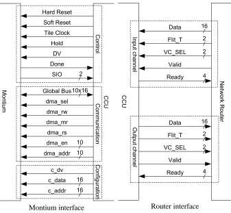
A tile consists of a network router, a tile processor and a processor-network interface: the CCU. The in-terfaces between these components are shown in figure 2.1. Per component, we will explain the interface signals.
2.1.1 Network router
The network interface consists of two identical unidirectional physical channels. Several packets can be
sent in parallel via the channels, by making use of virtual channels [4]. Each packet has its own virtual channel (indicated by VC_SEL in figure 2.1) and these virtual channels are multiplexed in time. Data
2. Environment and Requirements
! " #$%#&
'
#$
#& #& #$
Montium interface
!
!
" #
!
!
" #
Router interface
Figure 2.1: CCU interfaces
indicate whether it can receive data. For this indication, the Ready signal is used. The sender indicates a
data transfer with the Valid signal.
Because of the maximum of 4 virtual channels, each virtual channel gets at least 25% of the bandwidth
of the entire channel which results in a network with a guaranteed throughput.
Alternatively, due to interface compatibility a circuit-switched NoC [20] can be connected. This router will include a small interface to fit the CCU. The only difference for the CCU will be the fact that no
routing information needs to be added to packets.
2.1.2 Tile Processor
The Montium TP has three sub-interfaces with the CCU. The configuration interface uses
straight-forward address/data connections (c_addr and c_data) combined with a valid signal (c_dv) to indicate that the configuration interface currently contains valid configuration data. The configurable components in the Montium TP are mapped in a 16-bit address range and the configuration data width is 16-bit also.
For the data communication, the Montium TP has ten bi-directional global buses (GB). These buses are 16-bit wide and can be connected to each of the ten Montium memories. The CCU is capable of directly reading or writing the memories by using the dma interface of the Montium. When the dma_sel signal
is asserted, the CCU gets all permissions to access the memories. Each bus is then connected to one memory (i.e. bus 1 is connected to memory 1). The dma_en signal indicates which of the memories are
2.2. Requirements for the CCU
remaining dma signals dma_mr and dma_rs are used for a specific addressing of internal components of the Montium.
The third sub-interface contains the control and handshake signals needed to start the processing and synchronize the CCU with the Montium TP. The CCU is capable of halting the Montium TP by asserting
the hold signal and synchronization of the Montium TP with the CCU is done via the DV and Done signals, while the SIO signals are used by the Montium TP to control the CCU for streaming.
2.2
Requirements for the CCU
The CCU serves the tile processor by performing data oriented actions. Amongst them, we can
distin-guish the following actions:
• Loading and retrieving data to and from the tile memory • Configuration of the tile processor
• Start, stop and reset the tile processor
For loading and retrieving data, the CCU has to support both block based and streaming data. When a
block of data is transferred, small packets with fixed length are transmitted using guaranteed throughput and best effort. When the streaming mode is used, all the data is sent using a packet of infinite length.
Using a tile based architecture, input data can come from multiple sources. The CCU has to be able to
shuffle this input and send it in a different order to the tile processor. Data coming from a certain source may have to be written to the tile memories in an exotic order: some algorithms require the input data to
be reordered in a specific pattern.
The CCU can configure the configuration registers in the tile processor. This (re)configuration can be
done always, but in order to prevent undefined behaviour the tile has to be stopped.
In order to prove that the execution of typical multi-media applications on a heterogeneous SoC with coarse-grained reconfigurable components is feasible, we first need to prove that the interaction between
the tile processor and the NoC can be done in an efficient way.
Ultimately, the CCU has to be flexible enough to support data communication for the Montium TP while
CHAPTER
3
Messages
Using a black box approach, it is easy to control a tile without knowing anything about the internal architecture. Therefore, we introduce a small set of generic messages needed to initialise and control a
tile processor. This chapter descibes the structure of the few basic messages. To understand the message format, we first introduce the basic building blocks: flits.
3.1
Flits
A flit is an atomic unit of information used for data transfers between the network routers. A flit is a basic data word sent over a physical channel. During each clock cycle a physical channel can transport
one flit. In the packet-switched network, flits contain data equal to the channel width (16-bit) and have a flit type (2-bit). The network routers use two flit types for the routing of packets: Header flits contain the
routing information for a packet and a Tail flit terminatesa packet by deallocating the routing settings. Since the flit type is a 2-bit value, there are two additional types available for the tiles to communicate:
Command flits contain commands for the tiles and Data flits contain data.
3.2
Packets
The tiles communicate via the network by sending packets. A packet consists of a number of command
messages or data messages, which can be sent in a mixed order. Each packet starts with one or more header flits followed by an arbitrary number of data or command messages and finishes with one tail flit.
The number of the header flits at the beginning of the packet is equal to the number of routers the packet
has to pass. Each of these routers removes the first header flit from the packet and stores it for forwarding the following flits. Thus, the destination tile will receive the packet without the preceding header flits.
3. Messages
Messages can be sent in two forms: command messages control the tile, where data messages are used by multiple tiles to communicate. For a clear definition of the command message formats, we use a
regular expression notation. Table 3.1 shows the available regular expression syntax.
Table 3.1: Regular expression notation of packets
Notation Description
(A)(B) A followed by B (A)+ One or more times A
"D" Flit type (see 5.4 and later for symbol description)
3.3
Command messages
This section gives an overview of the commands messages available for the tile. To make the expressions
readable, we use the notation(data)to indicate a data flit and(addr)for address flits.
Generally, a command message should not break the processing of a data symbol. The execution of commands is done when an iteration of the process is finished. Besides, the network causes a variable
delay. Therefore, the proper execution moment of commands is very unpredictable.
3.3.1 Configuration
Reconfigurable systems contain a considerable amount of reconfigurable entities like configuration reg-isters or instruction memories.
The address mapping for these entities is entirely independent from the address mapping of the data memories in the tile. For a partly reconfiguration of the tile, specific entities can be addressed using the
configuration address map (see appendix A and [8]).
Configuration commands have the following structure:
con f ig == (cmd_c f g)(c f g_next)+; (3.1)
c f g_next == (addr)(data)+;
cmd_c f g == ”Cc f g”;
To configure at a specific address, after the configuration command an address has to be sent followed
by the configuration data. If a configuration has to be done at another address, the last data flit can be followed by a new address flit and more data.
3.3.2 Loading data
Loading data into the memories is comparable to configuring the tile’s registers, only differing in the bus
3.3. Command messages
Load data messages can have the same structure as configuration command:
load == (cmd_load)(load_next)+; (3.2)
load_next == (addr)(data)+;
cmd_load == ”Cload”;
Similar to the configuration, an address flit indicates the address where the following data has to be stored and new address flits indicate a new destination for more data.
3.3.3 Retrieving data
Any tile or interface (e.g. the CCN) can request data by sending a Retrieve data command. This command is followed by an address flit that indicates the offset address and a data flit containing the output channel and the number of results.
The command structure is:
retr == (cmd_retr)(retr_next)+; (3.3)
retr_next == (addr)(data);
cmd_retr == ”Cretr”;
Here also, a repetition of more address and data flits (retr_next) can be used to retrieve data from a new place.
3.3.4 Forwarding data
When the processes are mapped on the several tiles, they need to be "connected" by data streams.
How-ever, not every CCU is aware of the network locations of other tiles. Therefore, the CCN can set up the network connections using a Forward data command with the following structure:
f wd == ((cmd_ f wd)(head)+)+; (3.4)
cmd_ f wd == ”Cf wd”;
Basically, a Forward data command only contains a command for the CCU and additional routing
infor-mation for the creation of a new stream from the CCU to the next tile. This sequence can be repeated. For instance when a route via 5 tiles needs to be made, this would require routing information for each
tile and a command for each tile.
Any command other than the forward data command terminates the forwarding.
3.3.5 Run
After finishing the configuration and loading of the data, the CCU is notified with a Run command.
3. Messages
activate the tile by itself.
run == ”Crun”; (3.5)
Data flits following the Run command are interpreted by the tile as normal data, in contrast to other commands which use following data flits as arguments.
3.3.6 Wait
Whenever needed, the CCU can halt the tile by activating the hold signal. Using the Wait command, other tiles can halt the CCU and its tile. When a Run command is sent, the CCU and tile resume the execution of their instructions.
wait == ”Cwait”; (3.6)
3.3.7 Reset
Using a hardware reset would shutdown the entire chip, while only minor parts of it actually need to be reset. The Reset command is used to send a software reset. When the CCU receives a Reset command,
it asserts the soft reset signal to the Montium TP. Furthermore, the CCU itself is initialized to the reset state and the program counter, loop counters and flags in the sequencer are reset.
CHAPTER
4
Structural design
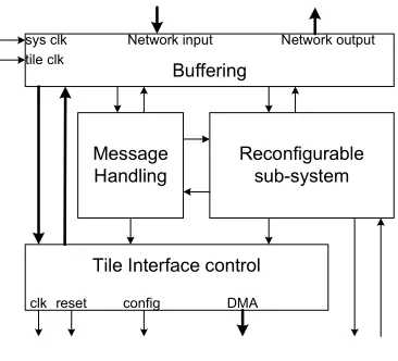
After defining the message protocol, the structure of the CCU can be organized. When we look at the requirements, there are several important issues that describe a structure. The most important properties
of the system are divided over 5 blocks (see figure 4.1):
• Buffering (data and controls passing the clock domain crossings have to be synchronized) • Data buses (parallel transport of data from the network to the tile processor and vice versa) • Message handler (execution of messages and controlling of the reconfigurable part) • Reconfigurable sub-system (reconfigurable entities for flexibility and energy-efficiency)
• Tile interface control (connections between the internal control signals and data buses to the tile processor)
Figure 4.1: Structural overview
In this chapter, each of these 5 blocks are discussed separately. From now on, for the main blocks abbreviations are used: MH (message handler), RSS (reconfigurable sub-system) and TIC (tile interface
4. Structural design
4.1
Buffering
Due to different clock speeds in the network and in the tile, data transfers need to be synchronised using
buffers. This can be done at two positions: at the Montium interface or at the network interface. Input buffering at the network side is needed because the wormhole router assumes that its output channels are buffered by the receiver. Therefore, it is a logical decision to place all synchronization buffers to the
network interface side. Moreover, given the fact that the tiles will never run at a higher speed than the network, it is very energy-efficient to reduce the part of the CCU running at the highest clock speed by
replacing it with a lower clock speed domain. This also contributes to the choice to move the buffering to the network side of the system.
For synchronizing, every input and output channel is connected to an asynchronous FIFO buffer with
separate read and write clock domains. Knowing that the global system clock and the local tile clock are in phase, no special synchronizing is necessary with the FIFO flags. Each channel has a dedicated buffer
for giving the CCU the flexibility to receive data from multiple sources and reordering these data in a specific way. A simple example of this is the case in which the CCU receives input data from source A and coefficients from source B. If blocks of n data words are processed with a coefficient C, only once in
the n clock cycles a new input C has to be received. The CCU has to make sure that the reading of these input happens in the right order and, therefore, it has to be able to shuffle the input data.
Figure 4.2: Input buffering and packet splitter
The buffer sizes are dependant on the difference between the two clock speeds. In case the both clock
domains run at the same speed, buffering will be used rarely, while buffering is quite important when there is a considerable difference in clock speeds (i.e. when the tile runs at a speed of 2 MHz compared to 100 MHz for the network).
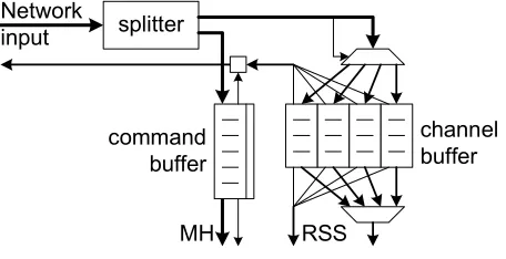
Network input can contain both command or data messages. As explained in section 4.4, it is useful to
store commands and data in separate buffers, as this makes the system more clear and structured and to prevent a wrong interpretation of commands. Therefore, a seperate command buffer is used to store incoming commands.
The deadlock problem caused by command and data messages sharing a single input channel can be prevented using a large command buffer compared to the channel buffers. However, this is not desirable,
4.2. Data buses
4.1.1 Packet splitter
The separation of packets into command messages and data messages is done by the packet splitter. The packet splitter directs the input data to the correct buffer.
Separation of command and data buffers gives the flexibility to read commands in parallel with reading data. Nevertheless, the CCU does not support simultaneous handling of commands and data. A great disadvantage of separating data and commands is the occurance of blocking. Whenever the command
buffer is filled, the packet splitter will immediately stop reading data from the network even if the data buffers are all empty: there is a small chance that one of the data streams contains a command, which
cannot be buffered in the command buffer because it is full already. In chapter 6.1 an analysis of this construction is given.
4.2
Data buses
Internal data transports use data buses. The simplest option is one bi-directional bus connecting the tile buses with the network channels. This does not support any parallellism, which is increases the design
simplicity. However, the CCU will significantly reduce the bandwidth of the tile which results in a high minimum clock frequency (so a large power dissipation).
Increasing the CCU bandwidth can be done by multiplicating the amount of internal buses. For a maximal
connectivity we need to connect each incoming and outgoing channel to the crossbar with a dedicated bus (resulting in a total of 8 internal buses). In order to control such a system, a lot of control signals need to be generated. Also, the separation of data and control flits may produce problems for the system.
A great disadvantage of multiple buses is the amount of wires and the accompanying area of those wires. Transporting signals over a large distance is not energy-efficient, so as few wires as possible should be
used. Like the first option of only one single bus, this option seems to be not very interesting for use1.
A trade-off of these options results in a design choice using two uni-directional buses. The advantage of two unidirectional buses over one bidirectional bus is the capability of simultaneously sending and
receiving data. Two buses provide the lowest level of parallellism and simplify the timing constraints compared to a maximal connected system with 8 internal data buses. Also, because only one channel
can drive the bus, the amount of selection signals are smaller compared to a more parallel version. With a limited internal connectivity, the energy consumption is reduced as much as possible. The choice of a 16-bit wide bus is a logical choice when the CCU is connected to the Montium TP and the network:
these connections are 16 bit wide.
4.3
Message Handler
A procedure is needed to execute incoming messages. To avoid a boot strap problem, the CCU has to
have some default configuration to be able to execute a configuration command.
1After separating the command and data buffers, this option at once became a very well suiting alternative. As can be read
4. Structural design
The first approach to tackle this problem is a sequencer with hardcoded instructions for the execution of commands. These hardcoded instructions can be placed in a small ROM and contain information
for the sequencer to manage the message. For the flexibility, the configurable part of the sequencer instructions is placed in SRAM memory, in a similary way compared to the Montium TP. Depending on
the command, the sequencer program counter is then moved to the associated address for instructions in the ROM for that command. However, this approach requires a very dynamic sequencer: it has to be able to read the input buffers, use the addresses to control the dma and configuration interfaces.
The message handling part is capable of reading incoming commands from the command buffer and executes them. The packets have a fixed format (see chapter 3.3) and therefore, all functionality is implemented in hardware. Each of the commands is parsed by a dedicated module (see figure 4.3). In
previous designs, a command interrupted the RSS and immediately switched to the execution of the command. Because of that, it is unknown what will happen with the current sample being processed and
in the worst case, this will mean data loss of one sample. To prevent data loss, the MH interacts with the RSS (RSS handshake in figure 4.3) to make sure that the data processing is not interrupted by incoming commands.
Figure 4.3: Message Handler
Besides handling incoming messages, the MH is responsible for the generation of internal control signals for the data buses and the network buffers. This is a necessity, because the system has to be controlled
by reliable components independent of its configuration.
4.3.1 State control
The state controller monitors the incoming messages in the command buffer. Commands change the
system state (see figure 4.4), but obviously the system should not respond on commands immediately. Therefore, the state controller and sequencer use a handshake mechanism (further explained in section 4.4.1).
The CCU has several operating modes represented by a central system state. This state machine deter-mines what has to be done with incoming messages, by enabling the RSS or the other modules in the
4.3. Message Handler
Figure 4.4: State diagram of the operating modes of the CCU
After a power-on reset, the CCU waits for commands in the ’reset’ state, in which no control modules are active. This state can also be entered by a reset command (soft-reset) from the CCN. To change
state control, messages are used as discussed in chapter 3.3. For example: from the ’reset’ state the ’configure’ state is reached using a ’configure’ command (enabling the configuration module); and with
the ’load/retrieve’ commands the ’load/retrieve’ state is entered (enabling the data module). When an invalid state transaction occurs, the system is switched to the reset state.
From each state almost each other state is reachable, to support an extremely flexible command handling. This, however, can give some troubles for the programmer, because a valid configuration is expected be-fore the system is activated. After completing the configuration, loading data or retrieving data processes,
a ’run’ command will switch the CCU to the ’run’ state. In this state, the RSS (chapter 4.4) is activated by a ’Run’ signal (figure 4.3). When a command is received in the ’run’ state, the tile finishes the current
computation and data transfers before the dedicated hardware modules can execute the command.
4.3.2 Loading and retrieving data
The data unit manages explicit data transfer commands. This component is used for actions such as changing specific memory addresses or debugging the tile program. The data unit consists of a state
machine capable of reading packets from the command buffer and generating addresses.
The system behaviour for loading and retrieving of data is almost similar. This was a direct motive to
combine the execution of these commands into a single module. Even though the data transfers are in an opposite direction, the generation of dma signals is done in an identical way.
4.3.3 Forwarding of data
With a packet-switched network on chip, the packets configure the network routers. We want the tiles
to have no consciousness about the environment and therefore, the streams connecting several tiles have to be created by a third party. Because the routers create an internal forwarding table, coupling input
4. Structural design
a shortcut within the CCU and send the actual headers through the CCU without changing them. This is done using the forward unit. The forward command has an argument containing the output channel; the
rest of the package is forwarded to the network, behaving as though it were an original packet sent by the CCU. For a description of the packet handling, see also chapter 3.3.
4.3.4 Configuration
Configuration data is written to the configuration interface of the Montium TP using the configuration unit. Depending on the selected address, specific parts of the CCU or Montium TP are configured. The configuration unit consists of a state machine capable of sequentially reading address and data flits. The
read address is stored in an address register and increased during every clock cycle.
4.4
Reconfigurable sub-system
The CCU has to support a wide range of communication schemes. A good solution for this flexibility
problem is the use of reconfigurable components.
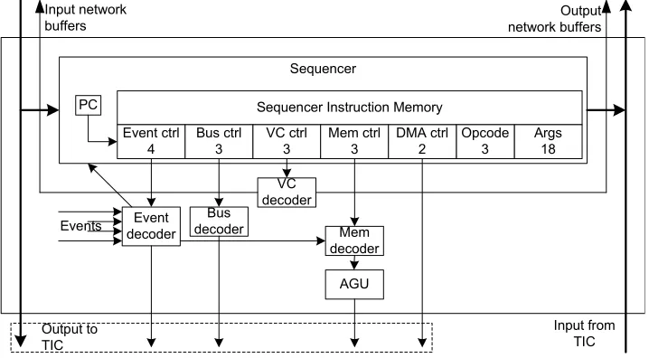
The reconfigurable sub-system is fully programmable. It provides the flexibility needed to execute typical data transferring algorithms. A sequencer is used to execute instructions. It is capable of executing
programs built out of blocking and non blocking conditions. Non-blocking conditions provide flexibility, while blocking conditions make sure that the system runs energy-efficient because the internal state is
kept fixed until the blocking resolves.
!" #
$ " % &
' ((
! " % &' ((
" ( ) ! "
)
Figure 4.5: Reconfigurable sub-system: the configurable entities of the CCU
The RSS reads data from the input data buffers and can write data to the output buffers. In the original
de-sign there was no separation between command and data buffers, so when the RSS was configured wrong it was reading commands as data. This is undesirable, so a dedicated command buffer was introduced.
4.4. Reconfigurable sub-system
Generally, only a very small subset of all possible configurations for the buses and network channels is used. In order to save chip area, several decoders are used to store the used configurations. When the
CCU is in Run mode, the sequencer instructions contain addresses for these decoders.
The reconfigurable part of the CCU is based on Montium TP components and design methodology.
Using a similar design makes a combined software development easier for the programmer.
An example program for the RSS is given in appendix A. It gives a clear overview of the decoder contents, that belongs to a pseudo-code data transferring algorithm.
4.4.1 Sequencer
The sequencer controls the entire CCU when it is in the ’Run’ state. The CCU sequencer is similar to the Montium TP sequencer, but the sequencer instruction memory and the instruction sets slightly differ.
As shown in figure 4.5, the sequencer is connected to the decoders and to the tile interface controller.
The programmer has to indicate at which instruction the sequencer can be interrupted, by setting break-points. The message handler interacts with the sequencer via the breakpoint signal and is able to react
on it. When the tile is processing data, the execution of incoming commands needs to postponed until the tile reaches a certain point where it is safe to stop the computation. Generally this will be at the end
of the program, but the system supports any number of specified breakpoints. The user can raise a flag to inform the MH that the sequencer has reached a breakpoint. If there are commands the sequencer will
be interrupted and otherwise it can continue its processing after lower the flag.
4.4.2 Event decoder
The CCU and Montium TP synchronize by using the handshake signals Done and DV. In every sequencer instruction, the event controller is addressed using the ’Event ctrl’ field. Each instruction in the event
decoder consists of a mask and a value-to-match for each event (Done, input data ready, output data
ready). If the masked events are equal to the required value, the condition is true and the RSS is
acti-vated. Unmasked events are always comparable and therefore, they do not contribute to the activation or blocking by the event decoder. In case the masked events do not have the required value, the sequencer is blocked until the required events occur.
The behavior of the event decoder is comparable to the predicated instruction behavior in Intel’s Itanium 2 [17]. The main difference is the blocking behavior of the event decoder as opposed to the non-blocking behavior of the Itanium (parallel execution of two possible solutions and eliminating one of both).
When streaming data, the Montium TP needs to notify the CCU when a certain event occurs. The SIO signals are used to signal the event decoder. The SIO signals from the Montium TP function as an address
input for the decoders, pointing to the lowest addresses in the decoder memories.
4.4.3 Bus decoder and VC decoder
Part of the sequencer instruction, the ’bus ctrl’ and ’VC ctrl’ fields, describe the interfaces between
4. Structural design
signals are used as addresses for the bus decoder and the virtual channel decoder to indicate data transfers. The combined bus decoder and vc decoder configuration settings describe a data transfer.
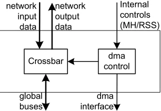
The bus decoder contains addressing information for the crossbar (section 4.5): each tile bus can be put in disabled, read or write mode. In the read mode, data from the tile bus is copied to the internal CCU
bus. Similarly, in the write mode, data from the internal CCU bus is copied to the tile bus.
The virtual channel decoder controls the reading of the input data buffers and the writing of the output buffers. Per configuration in the virtual channel decoder, one input and one output can be selected. Using
this construction one buffer can be selected per internal bus.
4.4.4 Memory decoder and AGU
The AGU creates addresses that are used by the sequencer when reading or writing data into or from
the Montium tile memories. This implies that the AGU will only be used when the sequencer is active. In order to save configuration space, a memory decoder is used to store a number of configurations for
the AGU. The ’MemInstr’ field in the sequencer addresses one of these configurations in the memory decoder.
Functionality supported by the AGU is the selection of offset addresses (called base address), which
can be increased with a selectable number (modify address) each clock cycle. Using this fields the tile memories can be addressed in exotic ways: blocks within the memory can be read, all even addresses can be written or even big jumps can be made within the address range. As an addition, the AGU supports
bit-reversing: by interchanging the most and least significancy of all bits, a simple increment during each clock cycle can produce exotic memory patterns. Typically, these patterns are used in FFT operations.
More information about the AGU can be found in appendix A and in [8].
4.5
Tile interface control
The tile interface controller manages the tile memory control. It converts addresses from the data unit
or AGU to DMA signals for the tile memory. The DMA controller is responsible for controlling the crossbar in order to manage the data flows between tile memories and internal CCU buses. The actual selection of a certain memory or register file is done using the DMA interface signals, as explained in
4.5. Tile interface control
CHAPTER
5
Realization
5.1
Hardware implementation
As part of the requirements, the implementation of the CCU has to be technology independent. This dependency limits the possibilities to optimise the design for a specific purpose, but it increases the
probability that the design will function correct when synthesized for an arbitrary technology. Chip area and power consumption depend on the gate count and therefore, mapping large storage on dedicated static rams reduces both area and power dissipation.
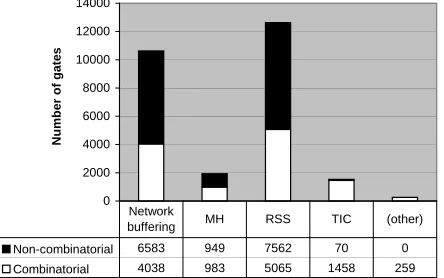
A synthesis run resulted in a system of roughly 27k gates1. Figure 5.1 shows the absolute gate count (both combinatorial and non-combinatorial) per component mentioned in chapter 4.
0 2000 4000 6000 8000 10000 12000 14000 N u m b e r o f g a te s
Non-combinatorial 6583 949 7562 70 0
Combinatorial 4038 983 5065 1458 259
Network
buffering MH RSS TIC (other)
Figure 5.1: Total gate count per component (absolute)
This data can also be viewed using pie chart 5.2, resulting in an overview of the area per component as a
percentage of the total area.
5. Realization
Network buffering 39%
MH 7% RSS 47%
TIC 6% (other) 1%
Figure 5.2: Total gate count per component (relative)
It is clear that the clock synchronisation (the network buffering) results in a substantial number of gates.
Due to their small sizes, implementation of the FIFO buffers in SRAMs will result in a higher gate count.
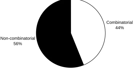
The relation between combinatorial and non-combinatorial gates as can be seen in figure 5.3 gives an indication about the reconfigurability of the system: the largest half of all gates form the
non-combinatorial part (i.e. storage elements). Even without the network buffering, more than half of the gates are non-combinatorial. When the sequencer instruction memory estimation is added to the total
non-combinatorial gate count of the RSS, this part will be roughly 10k gates.
Combinatorial 44%
Non-combinatorial 56%
Figure 5.3: Relation between Combinatorial and non-combinatorial gates
The CCU has been designed such that received messages are executed within 2 to 4 clock cycles. The average delay mainly depends on the difference in clock speeds of the tile compared to the network. When the clock speeds differ considerably, large input buffers can be used to improve the synchronization
and throughput.
5.2
Applications
An important category of applications for the Chameleon system is multi-media applications. In this sec-tion we discuss some wireless standard applicasec-tions described in [20]. The first and second applicasec-tions
5.2. Applications
the third application (UMTS) is based on W-CDMA. The kernel algorithm of OFDM systems is a Fast Fourier Transform (FFT) algorithm which can be done very optimal on a Montium TP. Since the fourier
transform is a typical operation that processes blocks of input signals which can be executed in parallel, it is an useful algorithm for testing the CCU. For the other computation blocks we make an estimation
for the clock frequency purely based on the bandwidth needed by each of these blocks.
5.2.1 HiperLAN/2
HiperLAN/2 is a wireless local area network access technology [5]. Every 4 µs an OFDM symbol (consisting of 64 complex samples) has to be processed. This processing is a succession of several
com-putations: a synchronisation (called frequency offset correction), a 64-point discrete fourier transform (inverse OFDM) and correction (equalization, phase offset correction and de-mapping) as displayed in figure 5.4. This sample processing is mapped on three Montium tiles [9].
Prefix removal Freq. offset correction Inverse OFDM Equalization De-mapping Phase offset correction
Montium Tile 1 Montium Tile 2
Montium Tile 3
(not implemented)
Figure 5.4: HiperLAN/2 receiver implemented on three Montium Tile Processors
The computation of operation frequency of each of the Montium tiles in figure 5.4 can be done using
the basic models for sending, receiving and processing as proposed in [11]. These models give several timing constraints for block-based processes. The models SCSP, PCSP and PCPP are used to analyse the HiperLAN/2 symbol processing2 done by an inverse OFDM operation (the operation mapped on
Montium tile 2 in figure 5.4.
Sequential communications and sequential processing (SCSP model)
Figure 5.5 shows the SCSP implementation of an OFDM operation. The process consists of data transfers
(here indicated by Din and Dout) and processing stages3(indicated by Si). During each stage a complex multiplication is done for each of the samples. In the Montium TP, the real and imaginary parts of the samples are divided over multiple memories. With this approach, 4 memories are used (memory 1
contains the real parts of the first 32 samples, memory 3 contains the complex parts of the first 32 samples and the last 32 samples are divided in over memory 5 and 7 a similar way). The arrow at Dinindicates a
2Both PCSP and PCPP models are not applicable to the current version of the CCU. However, to give an indication of the
efficacy of a more parallel version of the CCU, we show the results of these models
5. Realization
single word (containing either a real or complex part of a sample) being copied into the memories during the input phase. Consequently, during the first stage of an inverse OFDM operation, the input data are
read from the memories.
Figure 5.5: FFT operation in block mode (SCSP model)
Using the SCSP model only one word can be sent per clock cycle. Then, the communication time (the
time needed for Dinand Dout) is:
Tdata =
input samples per symbol+out put samples per symbol samples per word∗words per clock cycle
= 641+52 2∗1
=232 (5.1)
The FFT operation reads 64 input samples and computes the results in 6 stages. During each stage, 32 of
the 64 samples are multiplied with the other 32, resulting in 32 complex multiplications per stage. For each stage, 2 additional clock cycles are needed to fill and empty the pipelines.
Tcalc = stages∗
samples per symbol
2 +2
= 6∗34=204 (5.2)
These values can be found in table 5.1 as theoretical values. The communication overhead is4:
overhead = Tdata
Tcalc
= 232
204∗100%=113,7% (5.3)
The minimum required clock frequency can be calculated by using the total number of clock cycles
needed and the frame length:
fmin =
execution cycles f rame length
= Tdata+Tcalc 4µs
= 232+204
4∗10−6 =109 MHz (5.4)
Parallel communications and sequential processing (PCSP model)
By increasing the parallellism in the CCU (i.e. by transferring 4 words per clock cycle), the
communica-tion overhead can be decreased (equacommunica-tion 5.6, words per clock cycle=4). Still, data transactions cannot
5.2. Applications
be done in parallel with processing:
Tdata =
64+52 1 2∗4
=58 (5.5)
overhead = 58
204∗100%=28,4% (5.6)
Figure 5.6 shows the decrease in communication time compared to figure 5.5, when more inputs or outputs are addressed at the same time. Please note the different sizes of the communication blocks
compared to figure 5.5: data cannot be loaded into a memory while the contents are retrieved, because the current version of the Montium TP uses single ported memories. This reduces the maximum number of parallel input or output streams to 4.
Figure 5.6: FFT operation in block mode, with parallel reading or writing (PCSP model)
In this case, the resulting minimum operation frequency is:
fmin =
Tdata+Tcalc 4µs
= 58+204
4∗10−6 =66 MHz (5.7)
Parallel communications and parallel processing (PCPP model)
Another way to decrease the communication overhead is to execute the communication and processing in
parallel, as can be seen in figure 5.7. Again, the number of arrows indicates the number of streams. Note the crossed output arrows: the results are ordered with bitreversed addresses [8]. This is no problem,
assuming the receiving tile supports bit-reversing of addresses.
The streaming algorithm does not depend on the communication time, which means there is 0% com-munication overhead5.
Figure 5.7: FFT operation in streaming mode (PCPP model)
5. Realization
Streaming is very optimal for the clock frequency:
fmin =
Tdata+Tcalc 4µs
= 0+204
4∗10−6 =51 MHz (5.8)
After obtaining these clock frequencies for the inverse OFDM operation, we combine all the results into table 5.1. Similar to the previous equations, we can calculate the communication times and clock
frequencies for the frequency offset correction and the equalizer, phase offset and de-mapping. The theoretical and realized numbers of clock cycles for the communication part do not differ too much6. Note that the theoretical clock frequencies differ from table 5.1 due to the limitations in parallel reading
and writing the memories, caused by the CCU. For the frequency offset correction and the equalizer, no realization has been made yet.
Table 5.1: HiperLAN/2 implementation: theoretical and realization
Frequency Equalizer,
offset Inverse Phase offset,
correction OFDM de-map
Configuration time (clock cycles) (theoretical) 137 437 288
(realization) 212 556 373
Execution time (clock cycles) 67 204 110
Communication time (clock cycles) (realization) n.a. 240 n.a.
SCSP model (theoretical) 256 232 200
PCSP model (theoretical) 64 58 52
PCPP model (theoretical) 0 0 0
Clock frequency (MHz) (realization) n.a. 110 n.a.
SCSP model (theoretical) 81 109 78
PCSP model (theoretical) 33 66 41
PCPP model (theoretical) 17 51 28
Clearly, in this system the inverse OFDM operation is the bottleneck due to the big computation time. Therefore, the tile clock speed has to be at least 110 MHz, which is a best case situation (assuming the
input and output data streams are not blocked). Striking is the data transfer overhead in the frequency offset correction block: the communication overhead is almost 394% of the computation time. A more parallel communication would significantly decrease the required tile speed and therefore, reduce the
energy consumption.
For testing the CCU, an implementation of the Inverse OFDM algorithm is used. Due to the delays
occurring during handshakes between the Montium TP and the CCU, the realized communication times are slightly larger than the theoretical models. The realized system can be compared with the SCSP model, as a reference.
5.2. Applications
5.2.2 DRM
DRM (Digital Radio Mondiale) is a digital radio standard with a processing order similar to HiperLAN/2.
Every 26.6 ms a symbol has to be processed, so the communication requirements are a factor 6000 less compared to HiperLAN/2 [21]. Therefore, it is fair to state that if HiperLAN/2 can be implemented using
a Montium TP, the communication speed for symbols is not a critical bottleneck for a DRM receiver. Due to the relatively low bandwidth, the CCU is capable of sending and receiving the data fast enough for succesfull symbol processing, even at a very low clock frequency.
5.2.3 UMTS
In contrary to the two applications mentioned before, UMTS is a wireless application based on wideband code division multiple access (W-CDMA) instead of OFDM. The kernel contains a RAKE receiver which
can be mapped on the Montium architecture [14]. Our implementation is a streaming algorithm that simultaneously reads 4 input streams7, resulting in a bandwidth of about 320 Mbit/s.
Typically, a RAKE receiver implemented on the Montium TP would have to run at a clock speed of about 20 MHz. The network has to be capable of delivering the input data at a rate of at least 80 MHz and the output samples need to be delivered to the next tile for further processing, but the output data produced
by the RAKE receiver is roughly 12% of the input data8.
The bandwidth of the CCU is high enough if it runs at a clock speed of 80 MHz or faster, but since it does not support parallel streaming, a RAKE receiver cannot be implemented in the current version of
the CCU.
CHAPTER
6
Recommendations and Conclusion
An implementation of the CCU has been proposed and its performance was discussed on the basis of a typical algorithm for the Montium TP. During the project, we experienced some difficulties. This chapter
describes these difficulties, together with some possible solutions. Finally, we will give a conclusion about the system and the project.
6.1
Recommendations
During the implementation phase, some difficulties and weaknesses of the CCU design occurred. They do not change the system design, but some may require large parts of the system to be redesigned.
6.1.1 DMA interface
Perhaps the DMA interface has to be revised, due to some glitches on the global buses. The drivers of
the crosspoints in the crossbar seem to be very sensitive for short changes in their inputs and therefore the buses can behave in an undefined way for some very short interval (∼1200 ps)
6.1.2 Data transfer flexibility
The current design supports simultaneous streaming of one input and one output. However, some
al-gorithms need a multiple input or output streams. According to the performance estimations of section 5.2.1, the CCU now barely supports a 64-point FFT at the required bandwidth. The implementation of a UMTS receiver [20] is simply impossible because of the unsupported parallel input streaming. Extension
of crossbar increases parallellism but the configuration size will increase very fast as well. During DMA actions, each of the global buses is connected to one tile memory. Therefore, the crossbar in the CCU
6. Recommendations and Conclusion
tile memory.
Currently, the configuration settings for the data buffers and the Crossbar are saved separately (see section
4.4.3). For each bus 2 bits are needed to select the action (resulting in 20 bits per configuration) and the input and output buffer selection takes 6 bits. The total number of bits to store is then:
cold=dcb∗20+dvc∗6 (6.1)
where the current total number of bits to be stored is indicated by cold, dcbshows the depth of the decoder for the crossbar settings and dvcgives the depth of the channel buffer decoder.
As an alternative, the connectivity can be increased by connecting each input channel and each output channel to the crossbar. In that case, the crossbar configuration would consist of different types of
decoders. For each global bus, a read source has to be specified. This results in 30 bits per configuration (10 busses, 3 bits per bus to select the source channel). For each output channel, the source needs to be
specified. The amount of bits is 16 (4 outputs, 4 bits to select the source bus). Then the number of bits to store is:
cnew=dcb∗30+dvc∗16 (6.2)
where cnewis the total number of bits to be stored using the proposed connectivity.
We can take a simple example to compare these numbers. Assume we need to fill the memories for a FFT. This algorithm requires 4 memories to be filled with sample data, independent from the FFT size.
The current CCU requires 9 configurations1 for the crossbar to be able to independently read or write each memory, while the more parallel version only requires 3 configurations2. Comparing the results we see a relatively smaller configuration size for the suggested improvement3: cold=332 bits compared to
cnew=152 bits.
Generally, the parallellism in the CCU should only be limited by the number of inputs and outputs. A
scalable version will have a higher probability of survival.
6.1.3 Message formats
At the moment a command flit only contains 3 bits of command information, which means that the other
13 bits are not used. If possible, it would be better to add additional arguments in command flits to prevent overhead while sending packets.
6.1.4 Message handler
For each type of command, the message handler has a dedicated piece of hardware. Between these components, there are some similarities. Reducing the chip area by developing a more structured
mes-sage handler might improve the performance, while reducing the internal communication between these components. Due to less internal communication, it will be easier to understand the system structure.
1Decoder depths need to be a power of 2, so d
cb=16
2d
cb=4
3Assuming all the memory data comes from the same input channel, which means d
6.1. Recommendations
6.1.5 Command buffering
In the first version, we assumed that commands arrive at input channel VC0. This turned out to be very
awkward because this actually restricts the sequencer in the amount of usable input channels. Without this restriction, in some cases the sequencer read the commands and transmitted them to the Montium
TP. A better solution is to separate commands and data prematurely by using a packet splitter, which is designed in a very straightforward way. Yet, there is a problem that cannot be solved by using this approach. Because data and control are combined in one network, a situation in which data flits at
channel A are blocked because the input buffer for command flits (arriving at channel D) is full, is not very unlikely. Although it is possible to make agreements about the used channels, it is not unthinkable that multiple commands will disturb each other and cause the system to behave unpredictable. Therefore,
in the current version only one concurrent command is supported.
In a worst case situation, deadlock can occur. This typically happens when the sequencer has not reached
a breakpoint yet while a command message has arrived. Suppose the command length exceeds the command buffer size; the packet splitter will then stop reading network data and the sequencer will be
blocked until the packet splitter allows new data to pass to the channel buffers. This situation has to be reviewed very well and a better solution might be needed to use the system.
A solution for this problem would be the introduction of a configurable watch dog timer. If some error
occurs in the sequencer instructions, the watch dog timer can be used to prevent the tile from a deadlock situation where the sequencer waits for data while an incoming command blocks the data stream. The sequencer breakpoints are very useful to reset the watch dog timer, assuring the system does not block.
6.1.6 Interfaces
The CCU has been designed using specific interfaces of the Montium TP and the wormhole router. On the one hand this results in a well fitting system, but on the other hand the system is hardly adaptable for
other interfaces. The designs proposed in [6] and [13] make better use of a general interface, supporting the mapping of high-level programs to low-level designs [19].
6.1.7 Tile breakpointing
One of the most important additions that can be done is the implementation of a tile breakpointing and debugging system. When something happens with the data streams in the network on chip, the data will
not arrive at the correct tiles and therefore, the tiles will stall. If a certain tile seems to be malfunctioning, a system is needed to decide whether this is a transient fault or the tile is broken. It is desirable that this debugging can be done without adding debugging instructions in the source code, preventing a huge need
for knowledge about the hardware architecture by the user. In order to implement an useful debugging, a tile breakpointing system is needed. The current breakpointing system is more like a synchronization between the MH and the RSS, being not useful for debugging the tile. Probably, this will introduce
an interrupt signalling combined with an interrupt register somewhere in the tile address space. The breakpoints can be stored in a breakpoint register which contains a 1 bit field per sequencer instruction
6. Recommendations and Conclusion
provides a great flexibility, because the breakpointing can be reconfigured in 4 clock cycles at run-time (or less in a non-worst case situation). When this indicator is added to the sequencer instructions,
each instruction would have to be reconfigured resulting in a worst-case situation of 64 clock cycles of reconfiguration.
6.2
Conclusion
The first version of the CCU did not contain much hierarchy. At a certain moment, this resulted in a system without a clear structure. After grouping the components into five parts (the buffering, data
buses, MH, RSS and TIC) the top level design has become more transparent and contains only a few multiplexers together with some component instantiations. Each of the parts can now be updated while
on a higher system level no changes are needed.
With the current area and an added estimation for the sequencer instruction memory, the CCU is less than 10% of the area of a Montium TP. Due to unfavorable design choices concerning the decoder sizes,
roughly 10% of the entire system will be used rarely. This does not influence the statement that the total area is very acceptable concerning the requirements.
Throughput of the CCU is not very reliable: the execution delay of messages (2 to 4 clock cycles) is very acceptable, but the CCU does not guarantee the throughput of incoming command messages when the tile is executing its algorithm. Command messages can block data messages which, on their turn, block
the reading of command messages by the MH. This can result in a deadlock situation, if the user does not take the blocking into account while writing programs for the CCU.
The CCU may not have to be as flexible as proposed in order to support the Montium TP (or other tile
processors). Due to a limited time, as can be read in chapter 6.1 the functionality is slightly restricted. Although the reconfigurable part of the CCU eliminates control overhead in messages because the
desti-nation for data is known in advance, it does not eliminate inefficient used decoder space.