Available online: https://edupediapublications.org/journals/index.php/IJR/ P a g e | 3114
High Performance of CMOS 1-Bit Full adder cell Based
on Novel Techniques
P.Thirupathi & D.Sravani
1Dept of Electronics Engineering, CJITS, Jangaon, Warangal, TS, India, Email: [email protected].
[email protected]
1,Assistant professors in ECE Dept, CJITS Jangaon 2 Assistant.professor in ECE Dept CJITS, Jangaon Abstract:
In this paper we presented low spillage 10T one-piece full adders cells are proposed for versatile applications. The investigation has been performed on different process also, circuits strategies, the examination with spillage control. We presented another transistor resizing approach for 1bit full viper cells to decide the ideal rest transistor estimate which diminish the spillage power and region to limit spillage current. We have performed recreations utilizing Cadence Virtuoso 45nm standard CMOS innovation at room temperature with supply voltage of 0.71V. Recreations have been
moreover analyzed for different VDD.
Subsequently configuration rules have been inferred to choose the most reasonable topology for the plan highlights required. This paper moreover proposes a novel figure of legitimacy to practically think about 1-bit adders executed as a chain of one bit full adders. The CMOS spillage current at the process level can be diminished by some execute on profound sub micron technique. The circuit level strategy is lessened power utilization at abnormal state. In this paper we reproduce the 10T Adder utilizing numerous systems both circuit level, process level.
Key Word —Adder, CMOS, MOSFET Transistor Leakage and Threshold Voltage
I. Introduction:
Because of expanding the request of low power ICs for computerized Circuits, use in like palmtop PCs, cell versatile, and so on plan decisions which take into thought low power includes alongside other circuit highlights like speed, region, execution life time, precision and so forth. Augmentations are heart of computational circuits and numerous mind boggling number juggling circuits are in light of the expansion and it is frequently one of the speedlimiting components. Henceforth improvement of the snake both regarding speed as well as power utilization must be sought after. Amid the outline of a 1 bit full snake we need to settle on two decisions for various outline reflection levels. One is responsible for the viper's engineering actualized with the one-piece full snake as a building square. Alternate characterizes the specific configuration style at transistor level to actualize the piece full snake. The one-piece full viper utilized is a three-input two-yield square. The information sources are the two bits to be included, An and, B and the convey bit Ci, which is the counts of the past digits. The yields are the consequence of the whole operation S and the consequence of the of the convey bit operation Co. More in particular, the entirety and convey yield are given by
Available online: https://edupediapublications.org/journals/index.php/IJR/ P a g e | 3115 𝐶𝑜 = 𝐴𝐵 +(𝐴 + 𝐵)𝐶𝑖… … .... .2
From condition (2) it is clear that if A=B the convey yield is equivalent to their esteem Co = Ci and the full snake needs to sit tight for the calculation of Co. Up to this point, in the writing there have been a few examinations between full snake circuits. Be that as it may, in the previous work, no low-control topologies were acknowledged by any means, though in the last mentioned, new topologies which give off an impression of being promising isn't considered. In addition, the impacts of the interconnection parasitic of low-control full adders in were extricated from design just for the CMOS and CPL topologies, though they were as it were generally evaluated for alternate circuits. For these reasons, these evaluated comes about contrast from those exhibited in this paper. Aside from and, no precise examinations have been produced in the writing for different topologies, and recently proposed circuits are contrasted with existing ones by applying unique reproduction and examination techniques, and by utilizing diverse advancements. Henceforth, it isn't easy to think about exhibitions in a reasonable and unmistakably justifiable way. The investigation and correlation created here have been done as far as speed, control utilization and defer item. The examination, which likewise incorporates the most intriguing as of late proposed one-piece full adders, has been based on recreation keeps running on a Cadence domain by utilizing a 0.45nm procedure considering, since post format reproductions have been performed. Two distinctive outline methodologies have been utilized to measure each topology. The previous one is utilized to limit control utilization embracing least size transistors, the last one is least power-defer item by reasonable
transistor measuring. Execution for both arrangement systems has been additionally looked at for changed supply voltage values.
II the 10T Adder
Available online: https://edupediapublications.org/journals/index.php/IJR/ P a g e | 3116
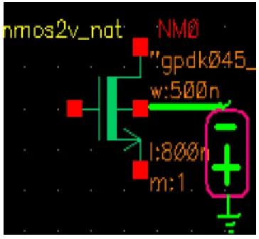
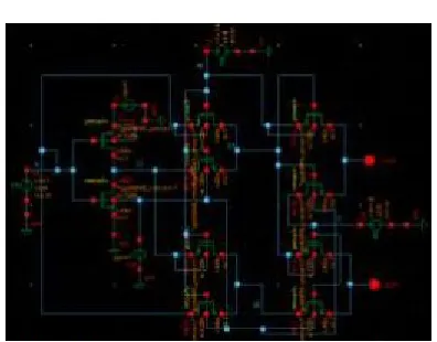
Fig-1 Ten Transistor Adder cell
In light of CMOS 0.45-nm process innovation, the proposed full viper is demonstrated to have the base control utilization and less power-postpone item by Rhythm reenactment contrasting and other earlier writing, the qualities of the novel half breed full snake demonstrates that the outline has the best power-delay item for complete flag. Because of the base time deferral of complete, the viper center extraordinarily enhances the general execution for a vast size of multi-bit snake. In dynamic method of operation the high Vt transistors are killed and the rationale doors comprising of low Vt transistors can work with low exchanging control scattering and littler exchanging time. In standby mode, the high VT transistors are killed subsequently removing the inside low Vt hardware.
III Low power 1-bit full adder
Frequently, Full viper is a piece of the basic way that decides the general execution of a framework. 1-bit full viper is a standout amongst the most huge parts of a processor that decides its throughput. In this paper I have outlined another 1-bit 10-transistor full viper which disseminates less power than the standard usage of full snake cell. The proposed snake is tried and contrasted and the high transistor tally furthermore, existing 10-transistor adders under the same conditions. The expansion of 2 bits An and B with C yields a SUM and a CARRY bit. The number likeness this connection is appeared as
𝑆 = 𝐴⊕𝐵⊕𝐶𝑖 = 𝐴𝐵𝐶𝑖 ̅̅̅̅̅̅̅̅̅̅̅̅̅̅̅̅̅̅̅̅
̅̅̅̅̅
+ 𝐴̅̅̅̅̅𝐵𝐶𝑖̅̅̅̅̅ +̅̅̅̅̅𝐴𝐵̅̅̅̅̅̅̅̅̅̅̅̅̅̅̅𝐶𝑖… .3
𝐶𝑜 = 𝐴𝐵 +(𝐴 + 𝐵)𝐶𝑖… … .… .... 4
The proposed snake executes conditions (3) and (4) utilizing reciprocal CMOS and MUX based outline rationale with just 10 transistors. The snake is valuable in bigger circuits, for example, multipliers notwithstanding the edge issue. The quantity of direct associations from VDD to the ground is lessened in the new outline to limit the power utilization because of short out current. Likewise the age of SUM from CARRY is maintained a strategic distance from as in the CMOS snake. Execution investigation of all the snake outlines is completed in 180nm, 90nm and 45nm CMOS innovation in rhythm. The execution is learned at control supply voltage of1.8V for 180nm, 1.0V for 90nm and 0.7V for 45nm at frequencies of 50MHZ.
IV CMOS Inverter Leakage Current
Available online: https://edupediapublications.org/journals/index.php/IJR/ P a g e | 3117
the two principle hotspots for control dissemination in CMOS circuits. Static power scattering happens because of spillage current when the transistor is for the most part off.
Fig-2. Static and dynamic power trends
The change in innovation scaling has presented large sub limit spillage current, consequently cautious plan systems are imperative with a specific end goal to lessen sub limit spillage current for low power plan .Spillage current rise in both dynamic and standby modes. It is recommended to turn off the spillage current at the point when the circuit is in standby shape. Innovation charts and power are appeared in fig-2. There are two noteworthy spillages current for control wastage in CMOS inverter
1. Sub limit (feeble reversal) spillage (ISUB)
2. Oxide burrowing Current (IG)
Where sub limit spillage current are clarify in numerical as
Where sub threshold leakage current are explain in mathematical as
where W and L denote the transistor width and length, µ represents the carrier mobility, VTH =
𝑘𝑡 𝑞 is the thermal voltage at temperature T, CSTH = CDEP+ Cit indicates the summation of the exhaustion locale capacitance and the interface trap capacitance both per
-initiated obstruction bringing down (DIBL) coefficient is the slant shape factor and is figured by condition 2
Hence the Oxide tunneling Current (IG or IFN) explain as
Where EOX is the field over the oxide; ØOX is the boundary tallness for electrons in the conduction band; and m* is the powerful mass of an electron in the conduction band of silicon. The FN is the current condition which speaks to the burrowing through the triangular potential boundary and is lawful for VOX >ØOX, where is the voltage drop over the oxide
V Leakage Reductions at Process Level
Available online: https://edupediapublications.org/journals/index.php/IJR/ P a g e | 3118
dynamic (exchanging) control (PD) and spillage control (PLEAK) are communicated as
Where α is the exchanging action; f is the operation recurrence; C is the heap capacitance. The substrate doping focus ought to be relatively expanded to diminish the consumption width. The hypothesis of consistent field scaling lies in scaling the gadget voltages and the gadget measurements by a similar factor, Not withstanding entryway oxide thickness and intersection scaling, another strategy is utilized to enhance short channel attributes is fine designing. By changing the doping profile in the channel locale, the dispersion of the electric field can be changed. The design is to improve the channel profile to limit the OFF-state spillage while augmenting the straight and immersed drive streams.
Fig-3(a) Leakage current of Adder
VI Leakage Reductions at Circuit Level
At the circuit level we can diminished spillage by a few strategy they self turn around biasing, different edge voltage, gated Vdd/Ground.
a) Self Reverse Biasing
The body impact in CMOS transistors, a littler width of the exhaustion layer prompts bring down VT. The switch biasing of CMOS transistor builds VT while on forward biasing of the COMS transistor VT diminishes. And furthermore in CMOS edge voltage increments with expanded doping of the channel however diminishes with connected inclination. In this way the current in the sub edge locale can be in part diminished by invert biasing. Condition (10) measures the back-entryway inclination parameter as capacity of the oxide capacitance and substrate doping level.
Where 𝑡𝑜𝑥 is gate oxide thickness, 𝑁𝑆𝑈𝐵 is substrate doping level q is unity electron charge
𝜖𝑜𝑥 is gate oxide permittivity and 𝜖𝑆𝑖 is Silicon permittivity.
Available online: https://edupediapublications.org/journals/index.php/IJR/ P a g e | 3119
Fig 4(b) 10T Adder circuit with reverse bias
Fig5 (a) Leakage current without reverse bias
Fig 5(b) Leakage current with reverse bias
b) Multiple channel doping
The threshold voltage is equals to the summation of the flat band voltage, twice the bulk potential and the voltage across the oxide due to the depletion layer charge.
The threshold voltage dependence on the doping density is illustrated with for both n-type and p-type MOSFETs with an aluminum gate metal.
Available online: https://edupediapublications.org/journals/index.php/IJR/ P a g e | 3120
The threshold of both types of devices is slightly negative at low doping densities and differs by 4 times the absolute value of the bulk potential. The threshold of NMOS increases with doping while the threshold of PMOS decreases with doping in the same way.
VII Simulation and Result
We reenact different Adder cell on rhythm device in diverse distinctive procedure and circuit parameter in 10T Adder and other and found that 10T Adder is the most noticeable low power utilization cell. The spillage control is diminished by abnormal state utilizing different methods. We have clear that VT is the most proper parameter for lessening spillage control and spillage current. By expanding doping and diminishing TOX diminished power utilization. The Equation-11 demonstrate that the limit voltage reliant on different parameters on Adder cell. Here we can see that the edge can changed by Ø, γ and η. They are effectively change by well building plan.
A variety of the level band voltage cause due to oxide charge will cause a decrease of both edge voltages if the charge is certain and an expansion if the charge is negative.
References
(1) Madhuri.Sada1, A.Srinivasulu2, C.Md.Aslam3 ―1 Bit Full Adder Cell for Reducing Low Leakage Current in Nano Meter Technology‖ International Journal of Engineering Research and Development, Volume 2, Issue 4 (July 2012), PP. 11-18
(2) Radu Zlatanovici, Sean Kao, Borivoje Nikolic,
―Energy-Delay of Optimization 64-Bit
CarryLookahead Adders With a 240ps 90nm CMOS Design Example,‖ IEEE J. Solid State circuits, vol.44, no. 2, pp. 569-583, Feb. 2009.
(3) Massimo Alioto and Gaetano Palumbo ―Analysis and Comparison on Full Adder Block in Submicron Technology‖ IEEE transactions on very large scale integration (VLSI) systems, vol. 10, no. 6, December 2002 pp 806-823.
(4) A. Shams and M. Bayoumi, ―A novel highperformance CMOS 1-Bit full-adder cell‖ IEEE Trans. Circuits Syst.—Part II, vol. 47, pp 478– 481, May 2000.
(5) H. Mahmoud and M. Bayoumi, ―A 10-transistor low-power high-speed full adder cell‖ in Proc. ISCAS’99, Orlando, FL, June 1999, pp. 43–46
(6) K. Chu and D. Pulfrey, ―A comparison of CMOS circuit techniques: Dif-ferential cascode voltage switch logic versus conventional logic‖ IEEE J. Solid-State Circuits , vol. SC-22, pp. 528–532, Aug. 1987
(7) K. Martin, Digital Integrated Circuit Design. Oxford, U.K.: Oxford University Press, 2000