Jiabin Wang* and Peng Gao
Abstract—By using a composite coupling structure for coplanar waveguide (CPW)/microstrip, a new dual-band bandpass filter (DBBPF) stacking inverted Y-shaped CPW resonators and rectangular ring resonators is proposed. Two resonant frequency bands are simultaneously excited by the CPW feed line. However, it can be convenient to tune individually. Several transmission zeros are realized to improve the selectivity of the filter and achieve wide stopband rejection. Good agreement between simulated and measured results demonstrates the validity of this DBBPF.
1. INTRODUCTION
With the rapid development of wireless communication, dual or even multiband filters play a key role in frequency-selecting and spurious suppression. Various design methods have been proposed to implement dual-band bandpass filters (DBBPF) by using microstrip line [1–3]. In recent years, miniaturization and integration of the circuit makes coplanar waveguide (CPW) technology has been investigated and improved because it has many advantages compared to the microstrip line, e.g., easy connections in series and shunt, low dispersion, without via hole, large rang of characteristic impedances, and the feasibility of simple coplanar-based on-wafer measurement [4]. Several dual-band CPW filters have been proposed [5, 6], while dual-band filters using a composite coupling structure for CPW/microstrip have rarely been reported.
This letter exhibits a novel dual-band filter with a CPW/microstrip composite coupling structure which excites two resonant frequencies simultaneously. Two transmission paths to RF signal operate at the center frequencies of 2.4 and 3.5 GHz for Wi-Fi/WiMAX applications. The excellent selectivity of two passbands and wide stopband rejection are achieved because several transmission zeros are realized in the stopbands.
2. DESIGN OF PROPOSED DUAL-BAND BANDPASS FILTER 2.1. Composite Coupling Structure for CPW/Microstrip Design
The three-dimensional view of DBBPF and composite coupling structure for CPW/microstrip are shown in Figure 1, the CPW transmission line and the microstrip transmission line is located on the top and bottom layer respectively. The left ellipse drawn in dotted line shows a configuration of the composite coupling structure for CPW/microstrip which is made up of three parallel CPW open-end stubs on top layer and a microstrip open-end stub on bottom layer. The right ellipse drawn in dotted line exhibits the lines I, II, III, IV, V and VI. Ignoring the effects of discontinuities between adjacent lines and considering the mutual couplings between lines II and III, lines I, II, III and IV are modeled as a section of two asymmetrically coupled parallel transmission lines [7]. In the same way, lines I, II, V and VI are
Received 19 November 2015, Accepted 14 December 2015, Scheduled 23 December 2015
* Corresponding author: Jiabin Wang ([email protected]).
Figure 1. Three-dimensional view of DBBPF and the composite coupling structure for CPW/microstrip.
modeled as another section of two asymmetrically coupled parallel transmission lines. Combining two sections of asymmetrically coupled transmission lines constitute the equivalent model of the composite coupling structure for CPW/microstrip. The composite coupling structure for CPW/microstrip not only connects two transmission paths in physics, but also excites two resonant frequencies simultaneously, which is the major challenge to design this DBBPF.
2.2. DBBPF Design
As shown in Figure 1, the proposed DBBPF is composed of two layers. On the top layer, two inverted Y-shaped CPW resonators are connected by impedance inverter (K-inverter) which represents the inductive coupling realized by shunt inductivity. On the bottom layer, two rectangular ring resonators are connected by admittance inverter (J-inverter) which represents the capacitive coupling between a pair of adjacent rectangular sides. Figure 2 shows the layout of the inverted Y-shaped CPW resonators and rectangular ring resonators. Resonators in the bottom and top layer belong to the distributed line resonator which is able to contain at least one oscillating electromagnetic field. The resonant frequency of the inverted Y-Shape CPW resonator is decided by the perimeter of itself, the first resonant frequency occurs whenL=λg/2, whereLis the perimeter of the inverted Y-shaped CPW resonator,λg is guided wavelength: λg = λ0/sqrt(εeff), λ0 is the free-space wavelength and εeff is the effective dielectric
constant for CPW line, it can be calculated by the formulas [8]:
εeff = 1 + (εr−1) 2
K(k1) Kk
1
K
k0 K(k0)
(1)
k0 =
s
(s+ 2∗w) (2)
k0 = 1−k2 0
(3)
(a) (b)
wavelength: λg =λ0/sqrt(εeff), εeff is the effective dielectric constant for microstrip line.
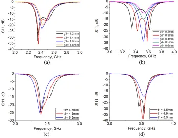
The distance g3 between two inverted Y-shaped CPW resonators is the most important factor of determining the coupling characteristic of them, the simulation results of two inverted Y-shaped CPW resonators with different distanceg3 are shown in Figure 3(a), which indicate that the inductive coupling is appropriate when g3 = 1.6 mm. So is the distance g4, which is the key impact on the strength of coupling between two rectangular ring resonators, the simulation results of two rectangular ring resonators with different distance g4 are shown in Figure 3(b), which state that the capacitive coupling is appropriate when g4 = 0.4 mm. The simulation frequency response of the two passbands with different lengtht1 are shown in Figure 3(c) and Figure 3(d), bandwidths of the two passbands are changed with different lengtht1, this indicates that the lengtht1 is the key parameter to impact on the Q-factor of the two passbands. The Q-factor of the two passbands can be controlled by the length t1.
Two sections of asymmetrically coupled transmission lines of the composite coupling structure can also be treated as two admittance inverters, which connect resonators to port and combine two passbands. Moreover, three transmission zeros are generated from the combination of two transmission paths to RF signal. There is a 180◦ phase difference in some frequencies after the RF signal pass the two paths, so the transmission zeros may be generated. Figure 4 shows the schematic of the dual-band
(a) (b)
(c) (d)
Figure 4. Schematic of the proposed DBBPF.
passband filter, it is the most straightforward way to implement a dual-band filter.
Two resonant frequencies are independently decided by the size of resonators, thus passbands are convenient to tune respectively. The length and width of inverted Y-shaped CPW resonators and rectangular ring resonators are key parameters to design the center resonant frequencies. The dimensions of the composite coupling structure have an impact on the strength of coupling between feed lines and resonators. The characteristic impedances of the input/output CPW feed lines are 50 Ω withw1 = 2.3 mm and g1 = 0.2 mm. Complete full-wave electromagnetic (EM) simulation tool is used to optimize these important parameters, as well as to obtain good performance of this DBBPF. The layout of proposed filter is shown in Figure 2. The final dimensions of the DBBPF are w2 = 1.6 mm, w3 = 1.0 mm, w4 = 1.0 mm, w5 = 1.0 mm, w6 = 6.9 mm, g2 = 0.5 mm, g3 = 1.5 mm, g4 = 0.4 mm, l1 = 12.6 mm, l2 = 9.9 mm, l3 = 15.8 mm, t1 = 4.9 mm,t2 = 6.3 mm. The overall area of the proposed filter is 40×25 mm2.
3. FABRICATION AND EXPERIMENTAL RESULTS
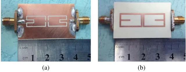
For the purpose of investigating the validity of proposed composite coupling structure, a DBBPF was designed and fabricated as the description given above. This filter is fabricated on Rogers RO4350B substrate with relative dielectric constant of 3.66 and a thickness of 0.762 mm. Photographs of fabrication are shown in Figure 5.
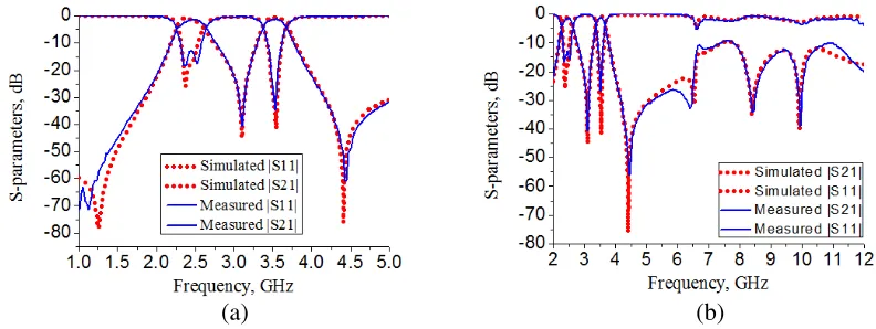
The measurement was carried out on an Agilent E8363B vector network analyzer (VNA). Figure 6(a) shows the simulated and measured frequency response of this DBBPF at the corresponding spectrum. The measured central frequencies are 2.45 and 3.55 GHz, with the fractional bandwidths of 15% and 8%. In the lower passband, the return loss and insertion loss are measured higher than 13 dB and lower than 1.57 dB, respectively. In the upper passband, the corresponding data are higher than 11 dB and lower than 1.22 dB. Transmission zeros located at 1.13, 3.10 and 4.42 GHz make the
(a) (b)
(a) (b)
Figure 6. Simulated and measuredS-parameters of the proposed DBBPF. (a) Narrow frequency range. (b) Wide frequency range.
selectivity of passbands better. Moreover, the isolation of two passbands is higher than 20 dB between 2.95 and 3.20 GHz. The properties of stopband rejection are shown in Figure 6(b), which is higher than 25 dB in the region of 4.15 to 6.4 GHz and is higher than 10 dB between 6.4 and 12 GHz.
4. CONCLUSION
A novel composite coupling structure for CPW/microstrip is proposed to connect and excite two passbands to implement a dual-band bandpass filter. This composite coupling structure is modeled as two sections of asymmetrically coupled transmission lines which can also be treated as admittance inverters to design DBBPF. The measurement of fabricated DBBPF shows simulated and measured results in very good agreement, which verifies the validity of this DBBPF.
REFERENCES
1. Tsai, L. C. and C. W. Hsue, “Dual-band bandpass filters using equal-length coupled-serial-shunted lines and z-transform technique,” IEEE Tran. Microw. Theory Tech., Vol. 52, No. 4, 1111–1117, 2004.
2. Zhang, Y. P. and M. Sun, “Dual-band microstrip bandpass filter using stepped-impedance resonators with new coupling schemes,” IEEE Tran. Microw. Theory Tech., Vol. 54, No. 10, 3779– 3785, 2006.
3. Zhang, X. Y., J. X. Chen, Q. Xue, and S. M. Li, “Dual-band bandpass filters using stub-loaded resonators,”IEEE Microw. Wirel. Compon. Lett., Vol. 17, No. 8, 583–585, 2007.
4. Wolff, I., Coplanar Microwave Integrated Circuit, John Wiley & Sons, Inc., Hoboken, NJ, USA, 2006.
5. Shi, J., J. X. Chen, and Q. Xue, “A quasi-elliptic function dual-band bandpass filter stacking spiral-shaped CPW defected ground structure and back-side coupled strip lines,” IEEE Microw. Wirel. Compon. Lett., Vol. 17, No. 6, 430–432, 2007.
6. Al-Khateeb, L. and O. Abu Safia, “Dual-band bandpass filter based on CPW series-connected resonators,”IET Electron. Lett., Vol. 49, No. 12, 761–762, 2013.
7. Lin, F. L., C. W. Chiu, and R. B. Wu, “Coplanar waveguide bandpass filter a ribbon-of-brick-wall design,” IEEE Tran. Microw. Theory Tech., Vol. 43, No. 7, 1589–1596, 1995.
8. Simons, R. N., Coplanar Waveguide Circuits, Components, and Systems, John Wiley & Sons, Inc., NJ, USA, 2001.