Complex Permittivity Estimation for Each Layer in a Bi-Layer
Dielectric Material at Ku-Band Frequencies
Lahcen Ait Benali1, *, Abdelwahed Tribak1, Jaouad Terhzaz2, and Angel Mediavilla3
Abstract—In this paper, a new measurement method is proposed to estimate the complex permittivity for each layer in a bi-layer dielectric material using a Ku-band rectangular waveguide WR62. TheSij -parameters at the reference planes in the rectangular waveguide loaded by a bi-layer material sample are measured as a function of frequency using the E8634A Network Analyzer. Also, by applying the transmission lines theory, the expressions for these parameters as a function of complex permittivity of each layer are calculated. The Nelder-Mead algorithm is then used to estimate the complex permittivity of each layer by matching the measured and calculated the Sij-parameters. This method has been validated by estimating, at the Ku-band, the complex permittivity of each layer of three bi-layer dielectric materials. A comparison of estimated values of the complex permittivity obtained from bi-layer measurements and mono-layer measurements is presented.
1. INTRODUCTION
Multi-layer dielectric materials are currently used in microwave integrated circuits and monolithic microwave integrated circuits [1, 2]. By choosing the electromagnetic properties and appropriate thickness for each layer, it is possible to synthesize bi-layer dielectric materials with new electromagnetic properties otherwise not found in a single mono-layer dielectric material [3].
Many measurement techniques have been developed and used in recent years to estimate the complex permittivity of monolayer dielectric materials [4, 7]. These include free space methods, cavity resonators techniques, and transmission line or waveguide techniques. Each technique has its distinct advantages and disadvantages. The free space methods are less accurate because of the unwanted reflection from surrounding objects [4]. The resonant cavity measurement technique is more accurate, but it has narrow band [5]. The Nicholson-Ross technique is widely used [6, 8] to determine the complex permittivity of dielectric material over a wide-band of frequencies accurately.
This technique has the disadvantage of having inaccuracy peaks for dielectric materials with low dielectric losses where the sample length is a multiple of half the wavelength of the rectangular waveguide [8]. To solve this problem, several researchers have combined the Nicholson Ross technique with nonlinear optimization techniques [8, 9]. However, these techniques are not used to estimate the complex permittivity of each layer in a bi-layer dielectric material in wide-band frequencies.
The aim of this work is to propose a new measurement method to estimate the complex permittivity for each layer of a bi-layer dielectric material at Ku-band. The bi-layer dielectric material is loaded in a rectangular waveguide WR62 with dimensions: a= 15.8 mm and b= 7.9 mm. The Sij-parameters are measured as a function of frequency using the Vector Network Analyzer and calculated as a function of the complex permittivity of each layer in a bi-layer dielectric material using transmission lines theory. To estimate the complex permittivity of each layer dielectric material with a specific prior knowledge of the thickness, the square sums of errors between the measured and calculated Sij-parameters are
Received 8 January 2018, Accepted 21 June 2018, Scheduled 12 July 2018 * Corresponding author: Lahcen Ait Benali ([email protected]).
minimized using a Nelder-Mead Algorithm [10]. The complex permittivity of each layer in a bi-layer dielectric material such as FR4-Teflon, FR4-Delrin and Teflon-Delrin is determined at the Ku-band frequencies.
2. THEORY
2.1. Direct Problem
This section presents the calculation of the Sij-parameters of a rectangular waveguide loaded with a bi-layer dielectric material as shown in Fig. 1.
Port1
z=-L0 z=0 z=L1 z=L1+L2 Port2
I II III IV
Figure 1. Rectangular waveguide loaded with a bi-layer dielectric material.
The bi-layer dielectric material consists of two layers, where the first layer has complex permittivity
εr1 and is located between transverses planes z = 0 and z = L1, and the second layer has complex
permittivity εr2 and is located between transverse planesz=L1 and z=L1+L2.
TheSij-parameter is found by analyzing the electric field at the sample interfaces. Assuming that only the dominant T E10 mode propagates in the loaded waveguide (see Fig. 1), the formulation of the
Sij-parameters can be expressed as a function of complex permittivity of each layer using transmission lines theory. In regions I, II, III and IV we can write the spatial distribution of the electric field for an incident field normalized to 1 in region I:
EI = 1 exp(−jγ0z) +A1exp(jγ0z) (1)
EII = A2exp(−jγ1z) +A3exp(jγ1z) (2)
EIII = A4exp(−jγ2z) +A5exp(jγ2z) (3)
EIV = A6exp(−jγ0z) (4)
whereγ0=
ω2 c2 −π
2 a2,γi =
εriωc22 −π 2
a2 and εri =εri−jεri withi= 1,2.
γ0, γ1 and γ2 are the propagation constants in vacuum, first layer and second layer, respectively; (ω) is the angular frequency; (a) is the dimension of the waveguide; c is the speed of light in vacuum. The constants Ai are determined from the boundary conditions.
Tangential component of the electric field is continuous at sample interfaces:
EI(z= 0) = EII(z= 0) (5)
EII(z=L1) = EIII(z=L1) (6)
EIII(z=L1+L2) = EIV(z=L1+L2) (7)
Tangential component of the magnetic field is continuous at sample interfaces:
∂EI
∂z (z= 0) = ∂EII
∂z (z= 0) (8)
∂EII
∂z (z=L1) = ∂EIII
∂z (z=L1) (9)
∂EIII
∂z (z=L1+L2) = ∂EIV
By application of these boundary conditions, we obtain the following matrix system: ⎡ ⎢ ⎢ ⎢ ⎢ ⎢ ⎣
e−jγ0L1 −ejγ1L1 −e−jγ1L1 0 0 0
γ0e−jγ0L1 γ1ejγ1L1 −γ1e−jγ1L1 0 0 0
0 1 1 −1 −1 0
0 −γ1 γ1 γ2 −γ2 0
0 0 0 e−jγ2L2 ejγ2L2 −e−jγ0L2 0 0 0 −γ2e−jγ1L1 γ2e−jγ1L1 γ0e−jγ0L2
⎤ ⎥ ⎥ ⎥ ⎥ ⎥ ⎦ ⎡ ⎢ ⎢ ⎢ ⎢ ⎢ ⎣ A1 A2 A3 A4 A5 A6 ⎤ ⎥ ⎥ ⎥ ⎥ ⎥ ⎦ = ⎡ ⎢ ⎢ ⎢ ⎢ ⎢ ⎣
−ejγ0L1
γ0ejγ0L1 0 0 0 0 ⎤ ⎥ ⎥ ⎥ ⎥ ⎥ ⎦ (11)
By solving this matrix system, we obtain the equation of S11 and S12 parameters as a function of the complex permittivities of each layer in the bi-layer material:
S11(εr1, εr1, εr2, εr2) = A1e−2jγ0L0 =e−2jγ0L0
d2+d1
d2−d1 (12)
S21(εr1, εr1, εr2, εr2) = A6e−jγ0(L0+L1+L2)=−2e−jγ0L0
γ0γ1γ2
(d2−d1).cosγ1L1.cosγ2L2 (13)
where:
d1 = γ1[γ0(γ2−γ1tanγ1L1.tanγ2L2) +jγ2(γ1tanγ1L1+γ2tanγ2L2)]
d2 = γ0[γ2(γ2tanγ1L1.tanγ2L2−γ1)−jγ0(γ1tanγ2L2+γ2tanγ1L1)]
To calculate S12 and S22 parameters as a function of complex permittivities of each layer in the bi-layer material, we assume that the fundamental mode T E10 is incident in region IV, and we follow the same procedure used to calculate the S11 and S21.
S12(εr1, εr1, εr2, εr2) = S21(εr1, εr1, εr2, εr2) (14) S22(εr1, εr1, εr2, εr2) =
d2+d1 d2−d1
(15)
where
d1 = γ2[γ0(γ1−γ2tanγ1L1.tanγ2L2) +jγ1(γ2tanγ2L2+γ1tanγ1L1)] d2 = γ0[γ1(γ1tanγ2L2.tanγ1L1−γ2)−jγ0(γ2tanγ1L1+γ1tanγ2L2)]
For mono-layer dielectric materials, we can chooseL1 = 0 andL2 =L, and in this case we have:
S11(εr, εr) = e−2jγ0L0 j(γ
2
0 −γ2)·tanγL
2γ0γ+j(γ20+γ2)·tanγL
(16)
S21(εr, εr) = e−jγ0L0 2γ0γ
[2γ0γ+j(γ02+γ2)·tanγL] cosγL
(17)
S12(εr, εr) = S21(εr, εr) (18)
S22(εr, εr) = j(γ
2
0 −γ2)·tanγL
2γ0γ+j(γ02+γ2)·tanγL
(19)
whereγ0=
ω2 c2 −π
2
a2 and γ =
εrωc22 −π 2 a2.
2.2. Inverse Problem
the complex relative permittivity such as εr = 1.5, εr = 0.005εr. The error function that we want to minimize with Fminsearch function is the square sums of errors between the measured and calculated
Sij-parameters written as follows:
f(εr1, εr1, εr2, εr2) =
ij
|Sijc−Sijm| (20)
3. NUMERICAL RESULTS
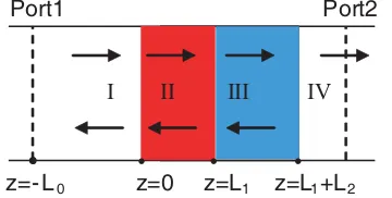
To validate the direct problem, theSij-parameters at the reference planes of the rectangular waveguide in Ku-band loaded by a mono-layer dielectric material Teflon (εr = 2.04, εr = 0.002) with thickness
L= 1.9 mm are calculated using the procedure described in Section 2.1 and simulated with HFSS (High Frequency Structure Simulator) software as shown in Fig. 2. It is seen from these results that there is an excellent agreement between calculated and simulated Sij-parameters.
12 13 14 15 16 17 18
Frequency (GHz) -1
-0.5 0 0.5 1
R
eal
(S
ij
) S11s S11c S21s S21c S22s S22c
12 13 14 15 16 17 18
Frequency (GHz) -1
-0.5 0 0.5 1
Im
ag
(S
ij
) S11s S11c S21s S21c S22s S22c
Figure 2. Simulated and calculated Sij-parameters in a rectangular waveguide WR62 (L0 +L = 6.7 mm) loaded by Teflon with thicknessL= 1.9 mm.
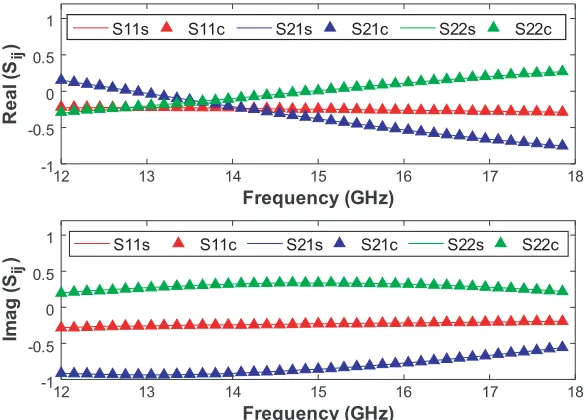
To validate the direct problem of bi-layer dielectric material, the Sij-parameters of a rectangular waveguide in Ku-band loaded by a bi-layer dielectric material formed by FR4 Epoxy (εr2= 4.5−j0.090)
with thicknessL2 = 1.5 mm and Teflon (εr1 = 2.04−j0.002) with thicknessL1 = 1.9 mm are calculated
using the procedure described in Section 2.1 and simulated by the use of HFSS software. As can be seen from the results shown in Fig. 3, there is a good agreement between calculated and simulated
Sij-parameters.
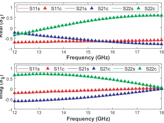
For the inverse problem, using the procedure described in Sections 2.1 and 2.2, the complex permittivity of mono-layer dielectric material and of each layer in a bi-layer dielectric material was determined in the Ku-band frequencies.
We consider the measurement system shown in Fig. 4. TheSij-parameters at references plane of a Ku-band rectangular waveguide WR62 loaded by a mono or a bi-layer dielectric material were measured using the E8634A Network Analyzer.
12 13 14 15 16 17 18 Frequency (GHz)
-1 -0.5 0 0.5 1
R
eal
(S
ij
) S11s S11c S21s S21c S22s S22c
12 13 14 15 16 17 18
Frequency (GHz) -1
-0.5 0 0.5 1
Im
ag
(S
ij
) S11s S11c S21s S21c S22s S22c
Figure 3. Simulated and calculatedSij-parameters in a rectangular waveguide (L0+L1+L2 = 6.7 mm) loaded by a bi-layer FR4(1.5 mm) and Teflon(1.9 mm).
Figure 4. The measurement system.
Table 1. Average complex permittivity and average relative error percentage on the real and imaginary parts of the complex permittivity at Ku-band.
Materials Measurement %Error
Bilayer Monolayer Monolayer Bilayer εr εr
FR4-Teflon FR4 4.4560−j0.0969 4.5065−j0.0981
<1.5% <7.2% Teflon 2.0361−j0.0035 2.0474−j0.0033
FR4-Delrin FR4 4.4560−j0.0969 4.5067−j0.1039 Delrin 2.9076−j0.0429 2.8812−j0.0445
12 13 14 15 16 17 18 Frequency (GHz)
1 2 3 4 5 6
R
eal
(r
) Teflon Delrin FR4
12 13 14 15 16 17 18
Frequency (GHz) -0.1
0 0.1 0.2 0.3
Im
ag
(
r
) Teflon Delrin FR4
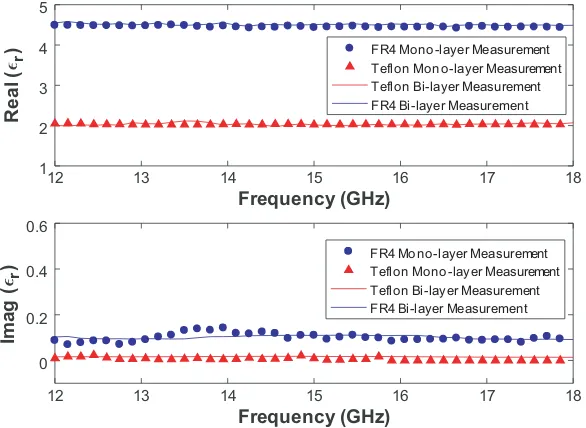
Figure 5. Complex permittivity of the mono-layers Teflon(1.9 mm), Delrin(2 mm) and FR4(1.5 mm) obtained from theSij measured using the inverse procedure with Nelder-Mead algorithm.
12 13 14 15 16 17 18
Frequency (GHz) 1
2 3 4 5
R
eal
(r
) FR4 Mono-layer Measurement
Teflon Mono-layer Measurement Teflon Bi-layer Measurement FR4 Bi-layer Measurement
12 13 14 15 16 17 18
Frequency (GHz) 0
0.2 0.4 0.6
Im
ag
(r
) FR4 Mono-layer MeasurementTeflon Mono-layer Measurement Teflon Bi-layer Measurement FR4 Bi-layer Measurement
Figure 6. Complex permittivity for each layer in the bi-layer FR4 epoxy(1.5 mm)-Teflon(1.9 mm) obtained from theSij measured using the inverse procedure with Nelder-Mead algorithm.
The results obtained for the complex permittivity of mono-layers by using the procedure described in this work are in good agreement. We can see that FR4 is a dielectric material with loss tangent about 0.02. However, the Teflon dielectric has a small loss tangent which is around 0.001. For the inverse problem, using the procedure described in Sections 2.1 and 2.2, the complex permittivity for each layer in the bi-layer dielectric material was determined in the Ku-band frequencies. The initial guess of the complex permittivity wasεr1 =εr2 = 1.5 andεr1 = 0.005εr1 andεr2= 0.01εr2. The values of dielectric
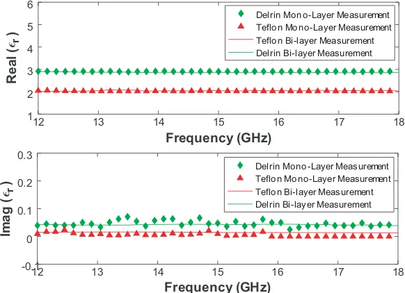
permittivity for each layer in the bi-layer FR4 epoxy-Teflon are determined and plotted in Fig. 6, those of FR4 epoxy-Delrin in Fig. 7, and those of Teflon-Delrin in Fig. 8.
12 13 14 15 16 17 18 Frequency (GHz)
2 4 6 8
R
eal
(r
)
FR4 Mono-Layer Measurement Delrin Mono-Layer Measurement Delrin Bi-layer Measurement FR4 Bi-layer Measurement
12 13 14 15 16 17 18
Frequency (GHz) -0.1
0 0.1 0.2 0.3
Im
ag
(r
)
FR4 Mono-Layer Measurement Delrin Mono-Layer Measurement Delrin Bi-layer Measurement FR4 Bi-layer Measurement
Figure 7. Complex permittivity for each layer in the bi-layer FR4 epoxy(1.5 mm)-Delrin(2 mm) obtained from theSij measured using the inverse procedure with Nelder-Mead algorithm.
12 13 14 15 16 17 18
Frequency (GHz) 1
2 3 4 5 6
R
eal
(r
)
Delrin Mono-Layer Measurement Teflon Mono-Layer Measurement Teflon Bi-layer Measurement Delrin Bi-layer Measurement
12 13 14 15 16 17 18
Frequency (GHz) -0.1
0 0.1 0.2 0.3
Im
ag
(r
) Delrin Mono-Layer MeasurementTeflon Mono-Layer Measurement Teflon Bi-layer Measurement Delrin Bi-layer Measurement
Figure 8. Complex permittivity for each layer in the bi-layer Teflon(1.9 mm)-Delrin(2 mm) obtained from the Sij measured using the inverse procedure with Nelder-Mead algorithm.
bi-layer materials made up from these mono-layers materials.
Table 1 presents the average values and average relative errors of the complex permittivities of each layer of material samples in the Ku-band calculated from monolayer and bi-layer measurements.
4. CONCLUSION
In this work, a new measurement method has been presented to estimate the complex permittivity of each layer in a bi-layer dielectric material with a specific prior knowledge of the thickness using a Ku-band rectangular waveguide WR62. TheSij-parameters are measured by Vector Network Analyzer and calculated as a function of complex permittivity of each layer using transmission lines theory. The Nelder-Mead Algorithm has been used to estimate the complex relative permittivity of each layer in a bi-layer dielectric material (or of a mono-layer dielectric material) by matching the calculated value with the measured value of Sij-parameters of a Ku-band rectangular waveguide, loaded by a bi-layer (or a mono-layer) dielectric material. The results obtained from bi-layer measurement are in good agreement with those obtained from mono-layer measurement. This method has been validated using three bi-layer dielectric materials such as FR4-Teflon, FR4-Delrin and Delrin-Teflon. The future work is to adapt this technique to estimate the dielectric properties of magnetic materials.
REFERENCES
1. Gupta, K. and P. S. Hall, Analysis and Design of Integrated Circuit-Antenna Modules, 247–248, Wiley, 1999.
2. Chakravarty, S. and R. Mittra, “Application of the micro-genetic algorithm to the design of spatial filters with frequency-selective surfaces embedded in dielectric media,”IEEE Trans. Electromagn. Compat., Vol. 44, No. 2, 338–346, 2002.
3. Deshpande, M. D. and K. Dudley, “Estimation of complex permittivity of composite multilayer material at microwave frequency using waveguide measurements,” NASA Langley Res., 212–398, 2003.
4. Ghodgaonkar, D. K., V. V. Varadan, and V. K. Varadan, “A freespace method for measurement of dielectric constants and loss tangents at microwave frequencies,” IEEE Trans. Instrum. Meas., Vol. 38, 789–793, 1989.
5. Ligthart, L. P., “A fast computational technique for accurate permittivity determination using transmission line methods,”IEEE Trans. MTT, Vol. 31, No. 3, 249–254, 1983.
6. Hasar, U. C., “Permittivity measurement of thin dielectric materials from reflection-only measurements using one-port vector network analyzers,” Progress In Electromagnetics Research, Vol. 95, 365–380, 2009.
7. Hasar, U. C., “Unique permittivity determination of low-loss dielectric materials from transmission measurements at microwave frequencies,”Progress In Electromagnetics Research, Vol. 107, 31–46, 2010.
8. Baker-Jarvis, J., Transmission/Reflection and Short-Circuit Line permittivity Measurements, National Institute of Standards and Technology, Boulder, Colorado, 1990.
9. Elmajid, H., J. Terhzaz, H. Ammor, M. Chabi, and A. Mediavilla, “A new method to determine the complex permittivity and complex permeability of dielectric materials at X-band frequencies,”
IJMOT, Vol. 10, No. 1, 34–39, 2015.
10. Nelder, J. and R. Mead “A simplex method for function minimization,” Computer SXSX Journal, Vol. 7, No. 4, 308–313, 1965.