Fault Tolerance Scan Based Logic BIST On
SRAM Using LFSR
Mr.N.Prakash Babu
1,Mr.K.Sundeep
2,Dr.M.Sri Nagesh
3 1Assoc. Professor, 2,3Professor & HoD1,2,3
Department of ECE, PACE ITS, Ongole, Prakasam District,Andhra Pradesh, India. E-Mail:[email protected], sundeep_k @pace.ac.in, srinagesh @pace.ac.in
Abstract: In addition, the manufacturing process in the nano-era which introduces new and complex failure mechanisms. Such failures are detected by requiring at-speed testing. Moreover, the electronic systems complexity has reached a level where the embedded memories accessibility utilizing external test equipment which is getting harder and costly, if not infeasible. Thus, memory testing which is high quality is crucial for improving the overall SoC quality. BIST (Built-in Self-Test) is the most common method in memory testing. Several implementations of BIST is proposed they are depends on either implementing a march element (ME), or on implementing a memory operation. We design a high speed scan based Built-In Self Test (BIST) in our proposed which is a serious examine for modern ICs. The circuit under test (CUT) transitions of signal may delay during test. Effects may be erroneously realized as delay faults with according to erroneous generation of test fails and maximize in the yield loss. Testing of memories of Semiconductor is increasingly significant due to the high density of current chips of memory and also due to older algorithms take so long for completion of their testing. Testing of SRAM is mainly depends on the concept of fault model utilized to faulty behaviours. To examine better methods for testing memories of semiconductor, March tests are of Order n, and then provide a systematic way to expand those tests.
Keywords: Built-in self-test, testing, fault- tolerance, reconfigurable system
1. INTRODUCTION
Mandatory part of any VLSI product of testing. In general a set of random pattern vectors are given as input to CUT .If the CUT produces same response for different test vectors then CUT in said to be good. Otherwise it is faulty IC. The most widely used approach for IC testing in ATE (Automatic Test Equipment). As chip design become complex day by day. The conventional approaches take more time to Test the IC [1]. The new process technology required to test the IC effectively. The most popular method to test the IC is BIST (Built In Self- Test).BIST is the technique with which IC Can be tested itself to decide whether IC in good (or) bad.
In the BIST the pseudo random test pattern are generated using linear shift register and their corresponding signature gets compared with golden signature. BIST in revolution way to test IC, which reduces testing time and test data storage. BIST was adopted to perform in field testing which can reduce testing cost as well as improving the quality of test at high speed [5]. The amount of test dateexchanged with the test in reduced. In addition large numbers of scan chains are configured. Hence the time required to apply a single test patterns reduces.
Now a days the most frequency used technique in logic BIST, which can take the form of either combinational LBIST or scan based LBIST. One of the fundamental DFT methodology logic Built in Self-Test (BIST).Generic scan based logic BIST architecture an shown in fig(1). The circuit is composed of combination logic and possibly embedded memories separated by multiple scan chains. The schematic diagram consist of pseudo-random, phase shifter circuit, the output response analysis blocks, Space Compactor MISR .In addition,
there are two more blockers which are pattern counters used for keep track of the number of cycles remained to fill the scan chains. Before using of BIST it has to be initiated through a boundary scan TAP Controller.
The actual test of the circuit consisting of several patterns for each pattern the shift counters counts (Nsc+Ncc) cycle ,where Nsc represents the number of cycle is the shift window in equal to the length of longest scan chain and NCC represents the number of cycles in capture windows is equal to one for a simple capture window. Hence it is necessary to configure the scan cells into large number of shallow scan to reduce the test application time. A systematically designed phone shifter circuit can be place between the LFSR and the scan chain inputs to eliminates structured dependency and allow a large number of scan chains to be driven by relatively short LFSR. Similarly space Compactor is used to compact a large numbers of scan outputs in to signature before feeding into MISR. Once the scan chains are loaded the multiplexers in the scan cells are placed in system mode for one cycle to capture the circuit response.
This sequence of events continues for each pattern. Once all the test phase are applied, the content of the MISR compared with reference signature to determine the status of the circuits.
2. LITRATURE SURVEY
To facilitate the presentation of the mechanism that involves Read Faults, the Read operation in SRAM memories is described. Figure 1a illustrates a SRAM memory cell with two supporting circuits: a pre-charge circuit and a sense amplifier. Pre-charge circuit sets the voltage level of the two bit lines at a fixed value (VDD). The Sense amplifier
detects the difference in the output voltage level of the two bit lines to determine the bit value (0 or 1). The details of the memory cell are illustrated in Figure 1b.The cell consists of two inverters (INV1 and INV2) and two access transistors (tn3 and tn4) that connects the cell with two bit lines BL and BLB.
Figure 1. SRAM Memory Cell
For example, assume the core cell shown in Figure 1b stores a logic '1' with node S at VDD and node SB at 0 V .To begin the read operation, the pre-charge circuit and sense amplifier needs to be enabled. This operation is necessary to charge the circuit to VDD. When the read operation is performed, the pre-charge circuit is turned off. At this point, bit lines are floating and remain at VDD. The word line (WL) of the access transistors tn3 and tn4 are then turned on. As the nodes BL and S are at the same potential
(VDD), no current flow occurs. Current flow occurs across nodes SB and BLB as they are at different potential. This leads to the discharge of bit line BLB. (VDD-ΔBL).
[image:2.596.205.398.423.572.2]A Sense Amplifier detects the voltage difference between two bit lines (ΔBL= VBL-VBLB) and determines the output value. If the difference is low it results in various read faults, including, Incorrect Read Fault (IRF), Read Destructive Fault (RDF), and Deceptive Read Destructive Fault (DRDF).
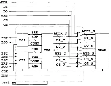
Figure 2. Block diagram of the BISD and SRAM cores.
The clock of SRAM can be shared by the core of BISD, hence there is no requirement for a separate test clock. The core of BISD contains three blocks such as
the Test pattern generator (TPG), controller (CTR), and fault site indicator (FSI). It contains set of multiplexers for the SRAM for switching among the BISD and modes of normal operation. This is performed by controlling the signal of BNS (BJSD/normal select). The test-se signal is for allowing the scan test for the circuit of BISD itself. In the mode of Scan- Test, the input of BSI considers the scan data of input and the output of BSO generates the scan data of output. On the chip the scan chain of the BISD can be linked to other scan chains.
Controller (CTR): The CTR gives test commands
for the Test Pattern Generator (TPG) that generates test patterns for testing the SRAM. It consists of two modes, i.e., the Test mode and Analysis modes. These modes are run by the input of BMS (BISD mode select). In the Test mode, the CTR provides a set of commands which is built-in to the TPG. The test algorithm is programmable and the shifting of test commands are done in from the input of BSI (BISD scan-in) in the Analysis mode.
Test Pattern Generator (TPG): The TPG
enabled, the TPG goes to the Initial state for initializing the session counter and the address counter. The session counter maintains track of the SRAM read/write operation (session) that is being implemented on the current address. The session value is utilized for obtaining the data of timing control that contains values of the write enable (WE) and output enable (OE) of the specified SRAM operation.
Fault Site Indicator (FSI): The FSI receives the information of error from the TPG and sends it to the output of BSO serially by utilizing a scan chain. When a detection of faulty word is done, the TPG enters in to the Wait state, and issues an error (ERR) signal, and sets the data of error operation (EOP) for the FSI. The FSI then sets the signal of BISD error flag (BEF) and provides the information about error to the output of BSO. After the completely shifting out EOP content, the continue (CONT) signal is by the FSI sets for allowing the TPG for continuing the execution of the current test command. If the scramble table is available, address mapping can be done in this stage by adding a decoder to the address part of the EOP register.
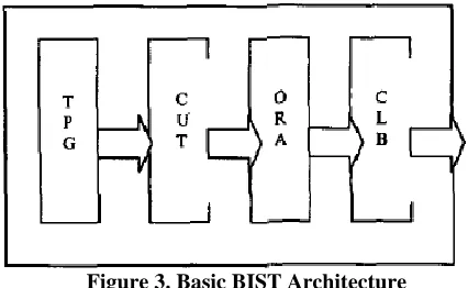
The testing mechanism is implemented using the BIST architecture. The test circuitry receives the stimulus to test the circuit, generates certain test patterns and compares the responses obtained with expected ones. Test Patterns are generated within the FPGA, by the TPG. The CUT receives the pattern from the TPG. Responses to the tests are evaluated on
chip. External operations are required only to initialize the built-in test and to check the test results from the circuit under test. We utilize pseudo exhaustive testing using LFSRs.
This test scheme has high fault coverage. An n-input combinational logic is tested by providing all possible 2n input patterns to the block. Even with high speeds of
clock, the time required for applying all the patterns may make BIST impractical for a circuit with larger values of 'n'. Therefore, we partition or segment the logic into smaller blocks with fewer inputs and test each block exhaustively. Fault coverage for pseudo-exhaustive testing and, it detects all stuck-at and bridging faults.
[image:3.596.208.421.435.566.2]The test patterns generated by the TPG are fed into the CUT sets, and the responses are fed into the Output Response Analyzer (ORA). The ORA compares the actual outputs obtained with the expected outputs. Any mismatch in values is an indication of the error that may be present in a particular set of interconnects lines. Each response obtained is stored in the LUTs of the Configurable Logic Block (CLB). After the completion of the test sequence, the LUT can be read and errors can be detected. All possible faults are detected in the interconnect network, the applied tests must verify that every segment of wire is able to communicate both a logic 0 and logic 1, which is achieved by utilizing the BIST approach.
Figure 3. Basic BIST Architecture
3. PROPOSED SYSTEM
The architecture consists of a memory array, data generator, address buffer, clock buffer, row address, column address, data in\out, BIST. The
memory array is the
Figure 4. Proposed System
Moreover, it is extremely susceptible to process variations and defect density. The column and row decoders are in charge of decoding the address; the most significant bits from the address lines will enable the right row while the least significant bits will enable the exact column. The memory cell array or consists of individual memory cells or bit cells arranged in a matrix form, where each bit cell is accessed through activation of the matching bit line and word line. The bit line will be enabled with the column decoder which is the least significant bit of the address. The word line will be enabled with the row decoder or most significant bit of the address.
Each bit cell can store one bit of binary data.
Each of the bit cells of the memory array is formed by a series of transistors which are called memory circuits. These circuits are designed to permit the access to the bit cell, by storing a value, by modifying the content of it, or by retrieving the value on it. The SRAM circuit can be visualized as a two inverter latch circuit with switches. This is because the memory circuit onlyhas two stable operating states: either the data is being held in the memory bit cell, or the data is being read from the memory circuit. This circuit has very low power dissipation and presents very good noise margin and switching speed. Therefore, it is a good candidate for high density SRAM arrays.
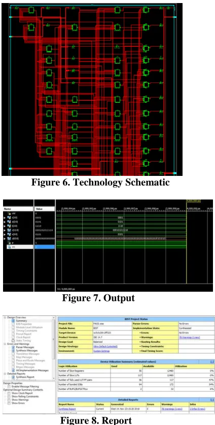
[image:4.596.203.361.473.671.2]4. RESULTS
Figure 6. Technology Schematic
Figure 7. Output
Figure 8. Report
5. CONCLUSION
We have proposed a programmable BISD design for embedded SRAM and an off- line fault diagnosis system. It supports March-based test and its diagnosis. The BISD circuit allows custom test commands to be applied for detailed diagnosis which including location and fault type of the SRAM. Our BISD design is cost effective, with low hardware overhead. Targeting embedded memory applications, our BISD is configurable at the RT level for various
memory architectures, timing
specifications, sizes, test requirements, etc. Our diagnosis system can report the types of the faulty cells in addition to their locations. This helps the SRAM designer as well as process engineers in improving the SRAM circuit and process for higher yield during the stage of development. With a test algorithm generator (such as TAGS) it also provides a trade-off between the diagnostic resolution and testing time. We are currently working on the development of efficient diagnosis algorithms and on-line diagnosis which will be incorporated in future versions of the BISD design.
This algorithm is quite fast and can provide
excellent solutions in short run- times. Experimental results indicate that this flow can save the designer many days of work by offering good BIST architectures which are complete in terms of logical and physical attributes. BIST designed here using March algorithm tests faster than the previously proposed ones. Compared with currently known microcode-based BIST techniques, the proposed design requires only one third of those microcode storages and the testing time is reduced. This BIST can be widely utilized for the embedded memory testing especially under the SoC design environment because of the superior extendibility and flexibility in applying different combination of algorithms of memory test.
REFERENCES
[1]
Ad J.van de Goor, “Testing Semiconductor memories: Theory and Practice”, 1999, ISBN 90-80 4276-1-62004, pp.430-440