ISSN(Online): 2320-9801
ISSN (Print): 2320-9798
International Journal of Innovative Research in Computer
and Communication Engineering
(An ISO 3297: 2007 Certified Organization)
Vol. 3, Issue 5, May 2015
Design of Double Tail Comparator Using Dual
Mode Logic in PTL Design
Elackiya.N
#, Swethaabraham
*M.E (VLSI Design), Dept.ECE, KarpagaVinayaga College of Engineering& Technology, Kanchipuram, Tamil Nadu,
India
Assistant Professor, Dept. ECE, KarpagaVinayaga College of Engineering& Technology, Kanchipuram, Tamil Nadu,
India
ABSTRACT: A logical circuit are either act in static mode or dynamic mode of operation. Recently, a novel dual mode logic (DML) family was proposed. This logic allows a circuit to operate in two modes:1) static 2) dynamic mode. DML gates, which can be switched between these modes on-the-fly, features very low power dissipation in the static mode and high performance in the dynamic mode. This paper shows that DML is applied in double tail comparator circuit designed in PTL design. The proposed methodology shows that delay and power achieved in DML circuit is optimized when compared to DML applied in standard CMOS design. The comparison and efficiency of proposed methodology is shown in tanner EDA v.13 tool.
KEYWORDS: Dual mode logic(DML), standard CMOS design , PTL design, delay, optimization
I. INTRODUCTION
Logic optimization and timing estimations are basic tasks for digital circuit designers. The logical effort method was for easy and fast evaluation and optimization of delay in CMOS logic paths. Because of its elegance, the LE method has become a very popular tool for designing and education purposes and is adopted to be the basis for several computer-aided-design tools [1]-[5].
Recently, we proposed the novel dual mode logic (DML), which provides the designer with a very high level of flexibility. It allows switching between two modes of operation: 1) static and 2) dynamic mode. In the static mode, DML circuit achieve very low power dissipation with some degradation in performance, as compared with standard CMOS. On the other hand, dynamic operation of DML gates achieves very high speed at the expense of increased power dissipation.
The main objective of this paper is to design double tail comparator based on dual mode logic in pass transistor logic design to achieve low power and high performance and shows comparison between optimization of delay between circuits. This paper shows that DML circuits in pass transistor design have less delay when compared to standard CMOS design. The simulations of circuits are achieved by using tanner EDA tool.
II. RELATED WORK
ISSN(Online): 2320-9801
ISSN (Print): 2320-9798
International Journal of Innovative Research in Computer
and Communication Engineering
(An ISO 3297: 2007 Certified Organization)
Vol. 3, Issue 5, May 2015
load distribution problem for circuit with fanout.[10].A general method in synthesis and signal arrangement in different pass-transistor network topologies is analyzed. Several pass-transistorlogic families have been introduced recently, but no systematic synthesis method is available that takes into account the impact of arrangement on circuit performance. In this paper a Karnaugh map based method that can be used to efficiently synthesize transistor logic circuits, which have balanced loads on true and complementary input signals. The method is applied to the generation of two-input and three-input logic gates in CPL, DPL and DVL. The method is general and can be extended to synthesize any pass-transistornetwork[11]. Differential double pass transistor logic unit Logic units are the building blocks of many important computational operations likes arithmetic, multiplexer demultiplexer,paritychecker,sumgenerator,etc...In this paper, a new differential CMOS logic unit circuit based on double pass transistors is proposed. This implementation is low power, low cost design with only 16 transistors to perform 8 logic functions. In order to evaluate the usefulness of the scheme, one bit Logic Unit was implemented and simulated. The proposed Logic Unit can operate at low voltages, yet giving quite a good speed[12].
III.PROPOSED SYSTEM A. Dual mode logic:
Dual mode logic(DML) which provides the designers very high level of flexibility. It allows on the fly switching between two modes of operation:1)static mode 2)dynamic mode. In the static mode of operation, the DML gates have very low power dissipation with moderate performance. When the DML gate is in the dynamic functional mode, they have much higher performance, at the cost of increased power dissipation.
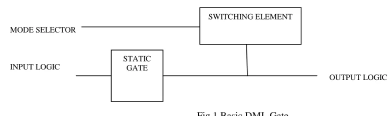
MODE SELECTOR
INPUT LOGIC
OUTPUT LOGIC
Fig 1 Basic DML Gate
The basic DML logic gate designed to operate in either static mode of operation or dynamic mode of operation consists: A static gate having one or more logic inputs, a single logic output and a switching element that is associated with the static gate.The switching element comprises of an input that is connected to a constant voltage, and another input for providing a signal used for mode selection, an output that is connected to a logic output of the static gate. The switching element can be configured to operate in either of the two modes by: i) disconnecting the static gate output from both the input that is connected to a constant voltage, and the other input for providing a signal used for mode selection, when the mode selection signal applies a constant voltage to the input used for providing mode selection signal, thereby selecting static mode of operation ii) Connecting the static gate output to both the input that is connected to a constant voltage, and the other input for providing a signal used for mode selection, when the mode selection signal applies a dynamic clock signal to the input used for providing mode selection signal, thereby to select dynamic mode operation. Switching the Dual mode logic gates between the two functional modes, static and dynamic, is performed by applying either a constant voltage or a dynamic clock signal at the mode selection input of the switching element.
B. Description of pass transistor logic design:
Pass transistor logicreduces the count of transistors used to make different logic gates by eliminating redundant transistors. These transistors are used as switches to pass logic levels between nodes of a circuit, instead of switches connected directly to supply voltages. For proper operation design rules restrict the arrangement of circuit.
There are two main pass-transistor circuit styles: those thatuses NMOS only pass-transistor circuits, like CPL, and
those that use both NMOS and PMOS pass-transistors,
DPLand DVL.
SWITCHING ELEMENT
ISSN(Online): 2320-9801
ISSN (Print): 2320-9798
International Journal of Innovative Research in Computer
and Communication Engineering
(An ISO 3297: 2007 Certified Organization)
Vol. 3, Issue 5, May 2015
B.(a)Double pass-transistor logic
However, since only NMOS transistors are used in CPL gates, the voltage swing at the end of a pass transistor
network has a swing from 0 to VDD - V TH; therefore PMOS transistors at the following static gates are not completely
off resulting in static power dissipation. This problem is usually solved by a PMOS level restorer transistor to pull up the node to VDD. The level restoreradds hysteresis to the gate and degrades the performance.Also, the delay of pass transistor networks increasesquadratically with the number of stages and as a result,some intermediate buffers should
be used to make strongV and ground. All these problems arise from the factthat NMOS transistors cannot pass
VDDfaithfully to theother side. The solution is using a complementary PMOStransistor in parallel with NMOS to
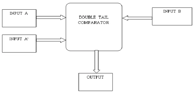
generate a strong VDDat the output. This structure is double pass transistor logic (DPL). DPL uses both PMOS and NMOS devices in the pass transistornetwork to avoid non full swing problems Double pass-transistor logic is shown to improve circuit performance at reduced supply voltage. Its Symmetrical arrangement and double-transmission characteristics improve the gate speed without increasing the input capacitance.The following fig.2 shows that DPL double tail comparator structure in which inputs are given as AA' and BB'.
Fig 2 Structure of DPL Double Tail Comparator
B.(b)Dual value logic
The main drawback of DPL is its redundancy, i.e. itrequires more transistors than actually needed for the realization of a function. To overcome the problem of redundancy, a new logic family, DVL is derived from DPL. It preserves the full swing operation of DPL with reduced transistor count. As introduced in DVL circuit can be derived from DPL circuits in three steps, consisting of:
Elimination of redundant branches
Signal rearrangement (resize)
Selection of the faster halves.
ISSN(Online): 2320-9801
ISSN (Print): 2320-9798
International Journal of Innovative Research in Computer
and Communication Engineering
(An ISO 3297: 2007 Certified Organization)
Vol. 3, Issue 5, May 2015
Fig 3 shows that dual value logic double tail comparator structure in which the input applied is AA' and B. Because this helps to execute the circuit in parallel, hence execution time will be reduced.
IV.DESIGN OF DML BASED DPL&DVL DOUBLE TAIL COMPARATOR
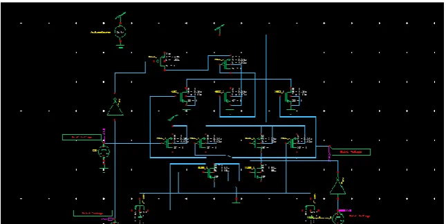
In double tail comparator circuit without using separate transistors, apply DML by interconnecting the transistors already there. For simpler circuit we should employ separate clocked transistors, for larger circuit by using same number of transistor we can employ dual mode concept. Thereby we can reduce area of chip. DML and its accompanying design methodology present a unique concept that enables an on-the-fly tradeoff between high performance(dynamic mode) and energy efficient (static mode) operation. TheDML methodology allows real time switching between these modes of operation from the scope of a single gate and upto a complete design block. This added flexibility provides the means to meet the delay requirements while minimizing power dissipationin proposed system, double tail comparator is designed in DPL and DVL, the inputs in DPL applied as
1. TwoNMOS branches cannot be overlapped on logic “1”s. Similarly, two PMOS branches cannot be overlapped on logic “0”s.
2. Pass signals are expressed in terms of input signals or supply. Every input vector has to be covered with exactly two branches. Hence the given inputs are AA´, BB´ the DVL based DML double tail comparator is consist of AB A´B inputs.
.
Fig 4 Schematic of DML Based DPL Double Tail Comparator
ISSN(Online): 2320-9801
ISSN (Print): 2320-9798
International Journal of Innovative Research in Computer
and Communication Engineering
(An ISO 3297: 2007 Certified Organization)
Vol. 3, Issue 5, May 2015
V. SIMULATION RESULT
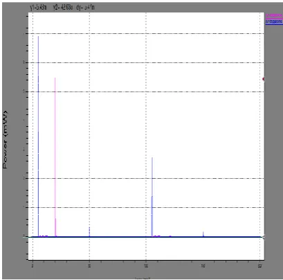
Simulations are carried out in tanner EDA the results shows that reduced delay, power and voltage drop
Fig 6 Delay waveform of DML based Fig 7 Power waveform of DML
DVL double tail comparator based DVL double tail comparator
Fig 8 Delay waveform of DML based Fig 9 Power waveform of DML based
ISSN(Online): 2320-9801
ISSN (Print): 2320-9798
International Journal of Innovative Research in Computer
and Communication Engineering
(An ISO 3297: 2007 Certified Organization)
Vol. 3, Issue 5, May 2015
Table 1: Table for Comparison of Standard CMOS Design and Pass Transistor Design
CIRCUIT DELAY VOLTAGE
DROP
POWER
DPL double tail
comparator
115.4ps 2V 14.54mw
DVL Double tail comparator
108.8ps 0V 12.98mw
DML based double tail comparator
199.2ps 2V 34mw
This table shows that comparison of results of DML based double pass transistor double tail comparator and DML based dual value logic double tail comparator. It shows that DVL circuit has optimized delay and less power. When we compare the results of these two design circuits, it shows that pass transistor design circuit have optimized results than standard CMOS design circuit.
VI.CONCLUSION AND FUTURE WORK
In the proposed design the DML concept is applied in different circuits such as CMOS inverter chain, conventional double tail comparator in standard CMOS design and shows that DML circuit has optimized results than conventional circuits. While applying this DML with pass transistor design like in DPL and DVL circuit, it is found that it has better performance and reduced power. That means by applying this DML concept with Comparator in pass transistor logic provides better result than standard CMOS design. Our work is concentrated on reduction of delay and reduced power consumption, and also in area efficiency. For this design of proposals we have used Tanner EDA 13.0v as simulation tool to show the performance analysis of this implementation.
In future development can improve the performance of the device and design by applying in any other families. Technology in electronics today is getting higher growth and become computationally intensive devices as the user interface has migrated to a fully multimedia experience.
REFERENCES
[1] .Itamar, Alexander Belenky and Alexander Fish, “Logical effort for CMOS-based dual mode logic gate,” IEEE Trans. Very Large Scale
Integr. (VLSI) Syst., vol.18, no.5,pp.689-696, May 2014
[2] I.E. Sutherland and R.F. Sproull, “Logical effort: Designing for speed on the back of an envelope,” in proc. Univ. California/Santa Cruz Conf.
Adv. Res. VLSI, 1991, pp. 1-16.
[3] I.E. Sutherland, B.Sproull, and D.Harris, Logical Effort—Designing Fast CMOS Circuits. San Matero, CA, USA: Morgan Kaufmann, 1999.
[4] M.A.Kabbani, D.Al-Khalili, and A.J.Al-Khalili, “Delay analysis of CMOS gates using modified logical effort model,” IEEE Trans Comput.
Aided Design Integer. Circuits Syst., vol.24, no.6, pp.937-947, jun. 2005.
[5] B.Lasbouygues, S.Engels, R.Wilson, P.Maurine, N.Azemard, and D.Auvergne, “Logical effort model extension to propagation delay
representation,” IEEE Trans. Comput. Aided Design Integr.Circuits Syst., vol.25, no.9,.1677-1684, sep.2006.
[6] P.Rezvani, A,H,Ajami, M.Pedram, and H.Savoj, “LEOPARD: A Logical Ef'fort-based fanout Optimizer for Area and delay,” in
Proc.IEEE/ACM IntConf.Comput.Aided Design, Dig Tech., Nov.1999, pp.516-519
[7] A.Morgenshtein, E.G.Friedman, R.Ginosar, and A.Kolodny, “Unified logical effort-a method for delay evaluation and minimization in logic
paths with I'nterconnect, “IEEE Trans. Very Large Scale Integr. (VLSI) Syst., vol.18, no.5,pp.689-696, May 2010
[8] M.-H.Chang, C.-Y.Hsieh, M.-W.Chen, and W.Hwang, “Logical effort models with voltage and temperature extensions in
super-/near-/subthreshold regions,” in Proc.VLSI Design Automa.Test(VLSI-DAT), Int.Symp.,Apr.2011,pp.1-4.
[9] I.Levi, O.Bass, A.Kaizerman, A.Belenky, and A.Fish, “High speed dual mode logic carry look ahead adder,” in Proc.IEEEInt.Symp.Circuits
Syst., May 2012, pp. 3037-3040.
[10] S.K.Karandikar and S.S.Sapatnekar, “Logical effort based technology mapping,” in Proc.IEEE/ACM Int.Conf.Comput.Aided Design,
ISSN(Online): 2320-9801
ISSN (Print): 2320-9798
International Journal of Innovative Research in Computer
and Communication Engineering
(An ISO 3297: 2007 Certified Organization)
Vol. 3, Issue 5, May 2015
[11] D. Markovic, B. Nikolic, V.G. Oklobdzija, “A general method in the synthesis of pass transistor circuits” in elseivermicroelectronics, pp.(2000)991-998
[12] ChirazKhedhiri, MounaKarmani&BelgacemHamdi, “a differential double pass transistor logic unit”,international journal of computer science
issue 2,no 1, march 2012
BIOGRAPHY
Elackiya.Nis a PG scholar in the M.E-VLSI Design,KarpagaVinayaga College of Engineering And Technology,Kanchipuram, Tamil Nadu,India. She completed B.E electronic & communication engineering in 2013 from PeriyarManiammai University, Thanjvur, TN, India.
Swetha Abrahamis a assistant professor in dept.ECE,KarpagaVinayaga College of Engineering And Technology, Kanchipuram, Tamil Nadu, India. She completed M.E-VLSI Design in Eshwari Engineering College,