Interdiction in Practice – Hardware Trojan Against a
High-Security USB Flash Drive
Pawel Swierczynski
∗, Marc Fyrbiak
∗, Philipp Koppe
∗, Amir Moradi
∗, and Christof Paar
∗†,
Fellow, IEEE
∗Horst G¨ortz Institute for IT Security, Ruhr University Bochum, Germany
†
University of Massachusetts Amherst, USA
{
pawel.swierczynski,marc.fyrbiak,philipp.koppe,amir.moradi,christof.paar
}
@rub.de
Abstract—As part of the revelations about the NSA activities, the notion of interdiction has become known to the public: the interception of deliveries to manipulate hardware in a way that backdoors are introduced. Manipulations can occur on the firmware or at hardware level. With respect to hardware, FPGAs are particular interesting targets as they can be altered by manipulating the corresponding bitstream which configures the device. In this paper, we demonstrate the first successful real-world FPGA hardware Trojan insertion into a commercial product. On the target device, a FIPS-140-2 level 2 certified USB flash drive from Kingston, the user data is encrypted using AES-256 in XTS mode, and the encryption/decryption is processed by an off-the-shelf SRAM-based FPGA. Our investigation required two reverse-engineering steps, related to the proprietary FPGA bitstream and to the firmware of the underlying ARM CPU. In our Trojan insertion scenario the targeted USB flash drive is intercepted before being delivered to the victim. The physical Trojan insertion requires the manipulation of the SPI flash memory content, which contains the FPGA bitstream as well as the ARM CPU code. The FPGA bitstream manipulation alters the exploited AES-256 algorithm in a way that it turns into a linear function which can be broken with 32 known plaintext-ciphertext pairs. After the manipulated USB flash drive has been used by the victim, the attacker is able to obtain all user data from the ciphertexts. Our work indeed highlights the security risks and especially the practical relevance of bitstream modification attacks that became realistic due to FPGA bitstream manipulations.
I. INTRODUCTION
In this section we provide an overview of our research and related previous works in the area of hardware Trojans and Field Programmable Gate Array (FPGA) security.
A. Motivation
As a part of the revelations by Edward Snowden, it became known that the National Security Agency (NSA) allegedly intercepts communication equipment during shipment in order to install backdoors [1]. For instance, Glenn Greenwald claims that firmware modifications have been made in Cisco routers [2], [3], [4]. Related attacks can also be launched in “weaker” settings, for instance, by an adversary that replaces existing equipment with one that is backdoor-equipped or by exploiting
Part of the research was conducted at the University of Massachusetts Amherst. This work has been also partially supported by the Hans L. Merkle Foundation.
reprogramming / updatability features to implant a backdoor. Other related attacks are hardware Trojans installed by OEMs. It can be argued that such attacks are particular worrisome because the entire arsenal of security mechanism available to us, ranging from cryptographic primitives over protocols to sophisticated access control and anti-malware measures, can be invalidated if the underlying hardware is manipulated in a targeted way. Despite the extensive public discussions about alleged manipulations by British, US, and other intelligence agencies, the technical details and feasibilities of the required manipulations are very much unclear. Even in the research literature most hardware Trojans are implemented on high level (e.g., King et al. [5]) and thus assume an attacker at the system design phase [6], [7].
B. Contribution
The goal of the contribution at hand is to provide a case study on how a commercial product, which supposedly pro-vides high security, can be weakened by meaningful low-level manipulations of an existing FPGA design. To the best of our knowledge, this is the first time that it is being demonstrated that a bitstream modification of an FPGA can have severe impacts on the system security of a real-world product. We manipulated the unknown and proprietary Xilinx FPGA bitstream of a FIPS-140-2 level 2 certified device. This required several steps including the bitstream file format reverse-engineering, Intellectual Property (IP) core analysis, and a meaningful modification of the hardware configuration. Our target device is a Data Traveler 5000, an overall FIPS-140-2 level 2 certified1 Universal Serial Bus (USB) flash drive from Kingston. It utilizes a Xilinx FPGA for high-speed encryption and decryption of the stored user data. As indicated before, we implant a hardware Trojan through manipulating the proprietary bitstream of the FPGA resulting in a maliciously altered Advanced Encryption Standard (AES)-256 IP core that is susceptible to cryptanalysis.
By the underlying adversary model it is assumed that the adversary can provide a manipulated USB flash drive to the victim. For accessing the (seemingly strongly encrypted) user data, the adversary can obtain the device by stealing it from the victim. Alternatively, it is also imaginable that a covert, remote channel can be implanted in the target system. Due to our manipulations, the adversary can easily recover all data from
the flash drive. It seems highly likely that the attack remains undetected, because the cryptographic layer is entirely hidden from the user. Similar attacks are possible in all settings where encryption and decryption are performed by the same entity, e.g., hard disk encryption or encryption in the cloud.
We hope that our contribution closes an important gap in the research literature between the (hardware-design oriented) FPGA Trojan community and insertions in real-world settings. Moreover, we believe our case study will be of interest to the security community at large with respect to the feasibility of low-level hardware manipulations. On a more technical level, our contribution demonstrates that FPGAs with unprotected (or poorly protected) bitstreams can pose a considerably security risk. In principle, the general attack vector is applicable against many other FPGA-equipped devices that perform security functions, e.g., routers or military equipments.
C. Related Work
Two lines of research, which have been treated mainly separately so far, are particularly relevant to our contribu-tion, i.e., FPGA security and hardware Trojans. FPGAs are reprogrammable hardware devices which are used in a wide spectrum of applications, e.g., network routers, data centers, automotive systems as well as consumer electronics and secu-rity systems. In 2010 more than 4 billion devices were shipped world-wide [9]. Surprisingly many of these applications are se-curity sensitive, thus modifications of designs exhibit a crucial threat to real-world systems. Despite the large body of FPGA security research over the past two decades, cf. [10], the issue of maliciously manipulating a commercial and proprietary third-party FPGA design — with the goal of implanting a Trojan that weakens the system security of a commercial high-security device — has never been addressed to the best of our knowledge. SRAM-based FPGAs, for which the configuration bitstream is stored in external (flash) memory, dominate the industry. Due to its volatility, SRAM-based FPGAs have to be re-configured at every power-up. Hence, in a scenario where an adversary can make changes to the external memory chip, the insertion of hardware Trojans becomes a possible attack vector. It is known for long time that an FPGA bitstream manipulation is applicable, but the complexity of maliciously altering the given hardware resources of a third-party FPGA configuration has not been addressed in practice. However, from an attacker’s point of view, the malicious manipulation of a third-party FPGA bitstream offers several practical hurdles that must be overcome. Amongst the main problems is the proprietary bitstream format that obfuscates the encoding of the FPGA configuration: there is no support for parsing the bitstream file to a human-readable netlist, i.e., the internal FPGA configuration cannot be explored. However, previous works have shown that Xilinx’ proprietary bitstream file format can be reverse-engineered back to the netlist representation up to a certain extent [11], [12], [13]. In general, it seems to be a safe assumption that a determined attacker can reverse-engineer all (or at least the relevant) parts of the netlist from a given third-party bitstream. As the next crucial steps, the adversary must detect and manipulate the hardware design. To
the best of our knowledge, the only publicly reported detec-tion and malicious manipuladetec-tion of cryptographic algorithms targeting a third-party bitstream is by Swierczynski et al. [14], which is also the basis of our work.
The related work by Chakraborty et al. [15] demonstrated the accelerated aging process of an FPGA by merging a ring-oscillator circuitry into an existing bitstream. Furthermore, the presented attack cannot change the existing parts (described as “Type 1 Trojan” in their work, e.g., the relevant parts of a cryptographic algorithm or access control mechanism) and hence is not applicable to undermine the system security of our targeted device. Thus, we cover and demonstrate the theo-retically described “Type 2 Trojan” defined by Charkaborty et al. [15]. Such Trojans are able to alter the existing hardware resources and expectedly require more analysis of the design. Another related work was done by Aldaya et al. [16]. The authors demonstrated a key recovery attack for all AES key sizes by tampering T-boxes which are stored in the Block-Ram (BRAM) of Xilinx FPGAs. It is a ciphertext-only attack and it was demonstrated that various previously proposed FPGA-based AES implementations are vulnerable to their proposed method.
One other practical hurdle for injecting a Trojan into an FPGA bitstream is an encrypted bitstream that ensures the integrity and confidentially of a design. The two market leaders Xilinx and Altera both provide bitstream encryption schemes to prevent IP theft and the manipulation of the proprietary bitstream. Nevertheless, it has been shown that those encryption schemes can be broken by means of side-channel analysis with moderate efforts [17], [18], [19]. In these attacks, the power consumption can be exploited during the encryption/decryption process to reveal the cryptographic keys under which the bitstream is encrypted. Subsequently, the bitstream can be decrypted, modified, and re-encrypted. Thus, current bitstream encryption mechanisms only provide moderate additional security against a determined adversary and would not hinder us to perform our presented bitstream modification attack for the most available FPGA device families.
Another relevant strand of research is the hardware Trojan. Malicious hardware manipulations, aka Trojans, have come in the spotlight of the scientific community after a report by the US DoD in 2005 [20]. A general taxonomy for Trojan insertion, functionality, and activation was introduced by Karri et al. [6]. Besides theoretical descriptions of hardware Trojans, the majority of research focused on the detection of malicious circuits. An overview of hardware Trojan detection approaches and their inherent problem of coverage is presented by Narasimhan et al. [7]. There are only very few research reports that address the design and implementation aspects of hardware Trojans. Most hardware Trojans (FPGAs and ASICs) from the academic literature are implemented using high-level (register transfer level) tools and hence assume a different, and considerably stronger attacker model — namely Trojan insertion during system design — compared to our low-level Trojan insertion.
interesting special case because an attacker can accomplish a hardware modification by altering the deployed bitstream prior to the FPGA power-up. The bitstream contains the configuration rules for programmable logic components and programmable interconnections. One can agree that it is arguable whether FPGA Trojans are “true” hardware Trojans. On the other hand, the bitstream controls the configuration of all hardware elements inside the FPGA, and attacks as shown in this paper lead to an actual change of the hardware configuration. Thus, even though they represent a corner case, we believe it is justified to classify FPGA Trojans as hardware Trojans.
It should be noted that our strategy is considerably different when compared to the BadUSB attack presented by Nohl et al. [21]. In our settings we needed to bypass the security mechanisms of a protected and special-purpose high-security USB flash drive to be able to alter the existing cryptographic circuitry of a proprietary third-party FPGA design. Compared to our contribution, the BadUSB attack mainly targets the reprogramming of unprotected low-cost USB peripherals that can distribute software-based malware, e.g., by emulating a keyboard device. Hence, the BadUSB attack is not related to the given and less explored threats of FPGA hardware Trojans.
II. PROCEEDING OFINSERTING ANFPGA TROJAN
In the following we assume that the attacker is able to intercept a device during the shipping delivery before it arrives at the actual end user. As indicated before, this is not an imagi-nary scenario as according to the Edward Snowden documents it is known as interdiction [1]. Subsequently, we present a method of how to explore third-party FPGA bitstreams.
A. Attack Scenario: Interdiction
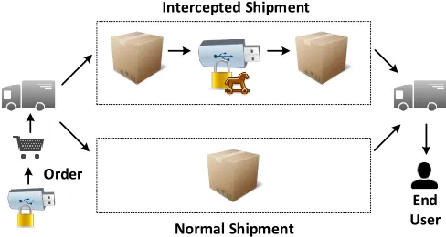
The process of interdiction is illustrated by Fig. 1. Ordered products (e.g., an USB flash drive) of an end user are secretly intercepted by an intelligence service during the shipment. The target device is modified or replaced by a malicious version, e.g., one with a backdoor. The compromised device is then delivered to the end user. Intelligence agencies can subsequently exploit the firmware or hardware manipulation.
According to the Snowden revelations, hardware Trojans are placed, e.g., in monitor or keyboard cables with hidden wireless transmitters, allowing for video and key logging [1]. Also, it can be assumed that a Personal Computer (PC) malware can be distributed with the help of a compromised firmware of an embedded device as recently demonstrated by Nohl et al. [21]. This can have severe impacts such as an unwanted secret remote access by a malicious third party or decryption of user data on physical access.
It is relatively easy to alter the firmware of micro-controllers, ARM CPUs, or other similar platforms if no read-out protec-tion is given or no self-tests are utilized.
In contrast, altering hardware such as an Application Spe-cific Integrated Circuit (ASIC) is a highly complex procedure. Recently, Becker et al. [22] demonstrated how a malicious factory can insert a hardware Trojan by changing the dopant
Normal Shipment Intercepted Shipment
Order
End User
Fig. 1: Interdiction attack conducted by intelligence services
polarity of existing transistors in an ASIC. However, this requires a different and considerably stronger attacker scenario than the one shown in Fig. 1, because the modification takes place during the manufacturing process. This is a time-consuming, difficult, and expensive task and therefore less practical.
On the contrary, at first glance, attacking an FPGA also seems to be similarly challenging because the bitstream file is proprietary and no tools are publicly available that convert the bitstream back to a netlist (for a recent scientific work see [23]). However, the recent work [14] has shown that a bitstream modification attack may indeed be successfully conducted with moderate efforts depending on the realization of the FPGA design.
In our case we conducted the scenario of Fig. 1 by manip-ulating the bitstream of an FPGA contained in a high-security USB flash drive that utilizes strong cryptography to protect user data. After the manipulated USB flash drive has been forwarded to and utilized for a certain amount of time by the end user, the attacker is able to obtain all user data.
B. Attack Scenario: Exploitation and Reconfigurability We want to highlight that interdiction is not the only realistic scenario for implanting an FPGA hardware Trojan. Modern embedded systems provide a remote firmware update mecha-nism to allow changes and improvements after the development phase. Such functionality exhibits an attractive target for an attacker to undermine the system security by means of exploits or logical flaws in the update mechanism. Thus, an attacker may remotely implant an FPGA hardware Trojan. To sum up, in several settings an attacker must not necessarily have physical access to the target device.
C. Exploring Third-Party FPGA Designs
in a meaningful way. Thus, the first important prerequisite is to learn the configuration from the proprietary bitstream. As mentioned above, previous works [11], [12], [13] have shown that the bitstream encoding of several Xilinx FPGAs can be (partially) reverse-engineered. Once the meaning of the bitstream encoding is revealed, an attacker can trans-late the bitstream to a human-readable netlist that serves for further analysis. This netlist contains all information of how Configurable Logic Blocks (CLBs), Input Output Blocks (IOBs), Digital Signal Processings (DSPs), or BRAMs are configured and interconnected. Roughly speaking, a bitstream file configures all the presented blocks in Fig. 2.
I/O CLB BRAM CLB DSP CLB I/O
I/O CLB BRAM CLB DSP CLB I/O
I/O CLB BRAM CLB DSP CLB I/O
I/O I/O I/O I/O I/O
I/O I/O I/O I/O I/O
Fig. 2: FPGA grid overview
The second challenging hurdle is the detection of (com-binatorial) logic within a large and complex circuitry. The detection is conducted at a very low level since the circuitry can be build by thousands of Look-up tables (LUTs) or Flip Flops (FFs), etc., which are interconnected by millions of wires along the FPGA grid. As long as it is unclear to the adversary how all those low-level elements (LUTs, FFs, wires, etc.) construct a circuitry and as long as he/she has no access to more information (e.g., the corresponding VHDL file), it is unlikely that he/she can successfully detect and replace parts of the logic. During a profiling phase, which only needs to be conducted once per FPGA device, the adversary creates and observes different variants of how specific functions are commonly synthesized, placed, and routed in the target FPGA grid (low-level device description).
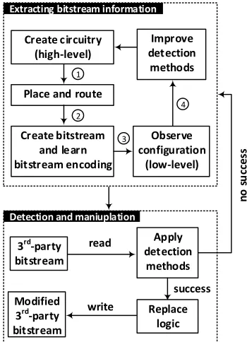
Once this investigation is conducted, the adversary knows how to detect specific circuitry from a given hardware configura-tion. If the relevant bitstream encoding part is unknown to the adversary, he/she can learn the bitstream encoding of a reference circuitry by creating and comparing the correspond-ing bitstreams of all possible configurations. This strategy is illustrated in Fig. 3.
In this work, we have practically verified the feasibility of our approach to implant the first practical hardware Trojan in the bitstream of a third-party design of a Xilinx Spartan-3E
Place and route
Create bitstream and learn bitstream encoding
Create circuitry (high-level)
Improve detection
methods Extracting bitstream information
Observe configuration
(low-level)
Detection and maniuplation
Apply detection
methods 3rd-party
bitstream
no
s
u
cce
ss
success
Replace logic read
write Modified
3rd-party bitstream
1
2
3
4
Fig. 3: Strategy of partially replacing an FPGA configuration
FPGA. The main strength of our presented attack vector is that it is practically possible to apply the presented modifications to a broader class of Static Random Access Memory (SRAM)-based FPGA devices. The attack itself can be performed in a short period of time (within one day) and thus is applicable in our presented interdiction scenario. This further emphasizes the attack’s practical relevance and its impacts regarding additional targets using an FPGA as a security device or trust anchor.
III. REAL-WORLDTARGETDEVICE
To demonstrate our FPGA Trojan insertion, we selected the Kingston DataTraveler 5000 [24] as the target, which is a publicly available commercial USB flash drive with strong focus on data security. This target device is overall FIPS-140-2 level 2 certified [8]. It uses Suite B [25] cryptographic algorithms, in particular AES-256, SHA-384, and Elliptic Curve Cryptography (ECC). All user data on our targeted USB drive is protected by an AES-256 in XEX-based Tweaked-codebook with ciphertext Stealing (XTS) mode. A PC software establishes a secured communication channel to the USB flash drive and enforces strong user passwords.
A. Initial Steps and Authentication Process
When plugging the USB flash drive into a USB port for the first time, an unprotected partition drive is mounted making the vendor’s PC software available to the user. Meanwhile, in the background, this software is copied (only once) to a temporary path from which it is always executed, c.f., the upper part of Fig. 7.
In an initial step, the end user needs to set a password. Afterwards, the user must be authenticated to the device using the previously-set password. This means that the key materials must be somewhere securely stored, which is commonly a multiple-hashed and salted password.
On every successful user authentication (mainly performed by the ARM CPU and the PC software), the protected partition drive is mounted allowing access to the user data. Any data written to the unlocked partition is encrypted with AES by the Xilinx FPGA and the corresponding ciphertexts are written into the sectors of the micro SD card as indicated in Fig. 7.
When unplugging the USB flash drive and for the case that an adversary has stolen this device, he/she is not able to access the user data without the knowledge of the corresponding pass-word. According to [24], after 10 wrong password attempts, the user data is irrevocably erased to prevent an attacker from conducting successful brute-force attempts.
B. Physical Attack — Revealing the FPGA Bitstream
To conduct an FPGA hardware Trojan insertion, we need to have access to the bitstream. Thus, in the first step we were able to remove the epoxy resin. Indeed, this procedure was much easier than expected. We locally heated up the epoxy resin to 200◦C (by a hot-air soldering station) turning it to a soft cover and removed the desired parts by means of a sharp instrument, e.g., a tiny screwdriver (see Fig. 4).
Fig. 4: Epoxy removal of Kingston DT 5000 with screwdriver
Fig. 5: Eavesdropping the bitstream of Kingston DT 5000 with opened case
By soldering out all the components, exploring the double-sided PCB and tracing the wires, we detected that an ARM CPU configures the Xilinx FPGA through an 8-bit bus. We also identified certain points on the PCB by which we can access
each bit of the aforementioned configuration bus. Therefore, we partially removed the epoxy resin of another operating identical target (USB flash drive) to access these points and then monitored this 8-bit bus during the power-up (by plugging the target into a PC USB port) and recorded the bitstream sent by the ARM CPU, cf., Fig. 5. Note that SRAM-based FPGAs must be configured at each power-up. By repeating the same process on several power-ups as well as on other identical targets, we could confirm the validity of the revealed bitstream and its consistency for all targets. We should emphasize that the header of the bitstream identified the type and the part number of the underlying FPGA matched with the soldered-out component.
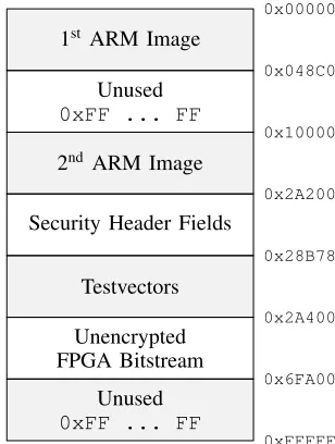
We also identified an Serial Peripheral Interface Bus (SPI) flash amongst the components of the PCB. As we have soldered out all the components, we could easily read out the content of the SPI flash. Since such components are commonly used as standalone non-volatile memory, no read-out protection is usually integrated. At first glance it became clear that the SPI flash contains the main ARM firmware (2nd ARM image). We also found another image (1st ARM image) initializing the necessary peripherals of the microcontroller. Furthermore, we identified that the bitstream, which we have revealed by monitoring the configuration bus, has been stored in the SPI flash, cf., Fig. 6.
Unused 0xFF ... FF
Unencrypted FPGA Bitstream
Testvectors Security Header Fields
2nd ARM Image Unused 0xFF ... FF 1st ARM Image
0xFFFFF 0x6FA00 0x2A400 0x28B78 0x2A200 0x10000 0x048C0 0x00000
Fig. 6: Address space layout of the SPI flash
Motivated by these findings we continued to analyze all other components of the USB flash drive and thus describe our results in the following.
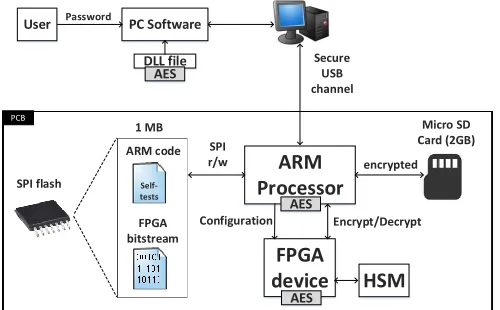
C. Overview and Component Details
• NXP LPC3131 with embedded ARM926EJ-S CPU op-erating at 180 MHz
• Xilinx Spartan-3E (XC3S500E) FPGA
• HSM from SPYRUS (Rosetta Micro Series II) providing ECDH, DSA, RSA, DES, 3-DES, AES, SHA-1, etc.
• 2 GB Transcend Micro SD card (larger versions also available)
• 1 MB (AT26DF081A) SPI flash
We revealed the layout of the circuit through reverse-engineering. The whole circuit is depicted in Fig. 7. This step was conducted by tracing the data buses of the PCB and by decompiling the PC software as well as the identified ARM firmware. Both executables were decompiled with Hex-Rays [26]. The resulting source code served for further reverse-engineering.
The main task of the identified ARM CPU (master device) is to handle the user authentication, while the Xilinx FPGA (slave device) is mainly responsible for the user data encryption and decryption. It should be noted that the FPGA is also partially involved in the authentication process and exhibits our main target for manipulation. We could not confirm the key storage location, but we assume that the key materials are securely stored in the Hardware Security Module (HSM), c.f., Fig. 7. As we demonstrate in this paper, we need neither any access to the key materials nor any knowledge of the key derivation function to be able to decrypt sensitive user data.
As stated before, both images (ARM CPU code and FPGA bitstream) were discovered in the SPI flash that are loaded and executed during the power-up of the USB flash drive.
FPGA
device
ARM
Processor
SPI flashPCB
ARM code
FPGA bitstream
Micro SD Card (2GB) 1 MB
HSM
Configuration Encrypt/DecryptSPI r/w
Self-tests
Secure USB channel PC Software
DLL file
encrypted User Password
AES AES AES
Fig. 7: Overview of revealed circuit of our target device
D. Unlinking FPGA Trojan from the Authentication Process
During our FPGA Trojan insertion, we identified several AES cores, as shown in Fig. 7:
1) AES core in the PC Software:used during user authen-tication.
2) AES core in the ARM code:used during user authenti-cation.
3) AES core in the FPGA:used during user authentication (partially) as well as for encrypting user data at high speed (main purpose).
If only the functionality of the FPGA AES core is manipulated, the target device would not operate properly anymore because all three AES cores need to be consistent due to the identified authentication dependencies. To be more precise, all three AES cores are involved in the same authentication process.
As our goal is to insert a hardware Trojan by manipulating the AES core of the FPGA, we first needed to unlink the dependency (of the AES cores) between the ARM CPU and the Xilinx FPGA, cf., Fig. 8. Therefore, we eliminated this dependency by altering parts of the ARM firmware, but we realized that any modification is detected by an integrity check. We identified several self-tests that are conducted – by the ARM CPU – on every power-up of the USB flash drive.
Further analyses revealed the presence of test-vectors. They are used to validate the correctness of the utilized cryptography within the system. The utilized self-tests are explained in Section VI-A in more detail. In Section VI-B, we demonstrate how to disable them and how to unlink the aforementioned dependencies.
To sum up, our intended attack is performed using the following steps:
1) Identify and disable the self-tests,
2) Unlink the AES dependency between the ARM and FPGA, and
3) Patch (reprogram) the FPGA bitstream meaningfully. Fig. 8 and Fig. 9 illustrate the impact of these steps. As can be seen, canceling the dependency allows us to alter the AES core and add an FPGA Trojan. The details of how we could
DLL
FPGA
ARM
AES AES
AES User
data
DLL
FPGA
Trojan
ARM
AES AES
AES User
data
Fig. 8: User authentica-tion (dashed) and user data (solid) dependencies before modification
DLL
FPGA
ARM
AES AES
AES User
data
DLL
FPGA
Trojan
ARM
AES AES
AES User
data
Fig. 9: User authentication (dashed) and data (solid) de-pendencies after modifica-tion
successfully alter the FPGA bitstream to realize a hardware Trojan are presented in Section IV. Below, we discuss why modifying a bitstream is more elegant for planting an FPGA Trojan than replacing the whole bitstream.
E. Modifying Bitstream vs. Replacing Whole Bitstream
challenging task. The attacker would need to further reverse-engineer and fully understand the whole FPGA environment (ARM code, data buses, protocols, etc.) and re-implement all functions to ensure the system’s compatibility. It even turned out to be the easier and faster approach, since we were able to modify this third-party IP core without the need to reverse-engineer or modify any part of the routing.
Thus, we only focus on detecting and replacing the relevant parts of the utilized FPGA design. By doing so, we secretly insert a stealth FPGA Trojan that turns the AES encryption and decryption modules into certain compatible weak functions, c.f., Section V.
F. Manipulation – Master vs. Slave
To be fair, on one hand the Kingston DataTraveler 5000 is not the best target device to demonstrate an FPGA hardware Trojan insertion because the embedded ARM CPU acts as the master device containing all control logic. The FPGA is merely used as an accelerator for cryptographic algorithms. In order to preserve the functionality of the USB flash drive with an active FPGA hardware Trojan the ARM CPU firmware – as previously explained – has to be customized too, i.e., the integrity check of the ARM CPU code needs to be disabled (explained in Section VI). At this point, the attacker can alter the firmware to not encrypt the user data at all, turning the device into a non-secure drive accessible to everyone. As another option, the attacker can secretly store the encryption key which would result in a conventional software-based embedded Trojan.
On the other hand, there are solutions which contain only an FPGA used as the master device [27]. Conventional software-based embedded Trojans are not applicable in those systems. Our attack is a proof of concept that FPGA hardware Trojans are practical threats for the FPGA-based systems where no software Trojan can be inserted. Our attack also highlights the necessity of embedded countermeasures on such systems to detect and defeat FPGA hardware Trojans.
IV. BUILDING THEFPGA TROJAN
In this section we shortly introduce the most common implementation styles to realize an AES encryption/decryption module. In addition, we present the information which can be extracted from the given bitstream file followed by our conducted modification on the AES-256 core. The impact of this modification – considering the utilized XTS mode of operation – is described in Section V.
A. Processing Methods of AES SubBytes
The SubBytes layer [28] of AES can be realized by various methods either in software or hardware. With respect to an FPGA we shortly explain the three most common schemes as they play an important role for our conducted manipulation:
1) Precomputation of S-box: Two 256-byte substitution tables denoted by S (AES S-box) and S−1 (inverse
AES S-box) are precomputed. These tables can be
either stored in the LUTs or in the block RAM of the FPGA.
2) On-the-fly computation: For a value x ∈ GF(28), the multiplicative inverse over GF(28) is derived and
followed by the affine transformation to construct the S-box outputS(x). A relatively small circuitry, e.g., the one proposed by Canright [29] can be used to realize an efficient and compact design.
3) Precomputation of T-boxes: S-box and MixColumns can be merged to build four T-box tables, each with 8-bit input and 32-8-bit output width [30]. These precom-puted tables are denoted byT0,T1,T2, andT3, which
considerably accelerate the encryption and decryption processes. To implement T-boxes, usually28 ×32bits
(i.e.,1024bytes) need to store one out of four T-boxes. Note that T-boxes are computed forx∈ {0,1, ...,255}
as follows.
T0(x) = 02◦S(x)||01◦S(x)||01◦S(x)||03◦S(x)
T1(x) = 03◦S(x)||02◦S(x)||01◦S(x)||01◦S(x)
T2(x) = 01◦S(x)||03◦S(x)||02◦S(x)||01◦S(x)
T3(x) = 01◦S(x)||01◦S(x)||03◦S(x)||02◦S(x),
where ◦ denotes multiplication in GF(28) using the
AES polynomialP(x) =x8+x4+x3+x+ 1and||
represents the concatenation. T-boxes are usually stored in block RAMs of the FPGA to achieve a compact and efficient implementation.
B. Analysis of the Extracted Bitstream
Based on the method presented in Section II, we could dump and analyze the initial memory configuration of each block RAM of the extracted bitstream. The Spartan-3E FPGA contains up to 20 block RAMs. We figured out that only 10 out of 20 block RAMs are used by the extracted FPGA design. We observed that the block RAMs are organized in a byte-wise manner fitting well to the structure of the AES state.
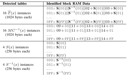
Our analysis revealed the presence of multiple instances of certain precomputed substitution tables. After investigating the extracted data in more detail, we obtained a structure for each table. We refer to the four identified tables whose details are depicted in Table I. Each substitution table stores 256 entries that can be accessed using the input x∈ {0,1, ...,255}. Our analysis revealed that the following precomputed substitution tables are stored in several block RAMs:
e
T(x) = 01◦S(x)||01◦S−1(x)||02◦S(x)||03◦S(x)
M C−1(x) = 09◦x||11◦x||13◦x||14◦x
S(x) = S(x)
S−1(x) = S−1(x)
In other words, we identified the tables which realize the inverse MixColumns transformation (M C−1(·)), the SubBytes
and inverse SubBytes (S(·) and S−1(·)). However,
e T(·) is not equivalent to any T-box (T0, . . . , T3), but exhibits a very
Detected tables Identified block RAM Data
000:S(00)||S−1(00)||02◦S(00)||03◦S(00) 16T(x)e instances 001:S(01)||S−1(01)||02◦S(01)||03◦S(01)
(1024 bytes each) . . .
0FF:S(FF)||S−1(FF)||02◦S(FF)||03◦S(FF) 000:09◦00||11◦00||13◦00||14◦00
16M C−1(x)instances 001:09◦01||11◦01||13◦01||14◦01
(1024 bytes each) . . .
0FF:09◦FF||11◦FF||13◦FF||14◦FF 000:S(00)
4S(x)instances 001:S(01) (256 bytes each) . . .
0FF:S(FF) 000:S−1(00) 4S−1(x)instances 001:S−1(01)
(256 bytes each) . . .
0FF:S−1(FF)
TABLE I: Identified substitution tables stored in block RAM
and03◦S(·)). In particularTe(·)combines the SubBytes and
MixColumns transformations, and thus has the same purpose as one T-box, but one remarkable difference is the storage of the inverse S-boxS−1(·). Note that all four T-boxesT0, . . . , T3
can be easily derived from Te.
C. Modifying the Third-Party FPGA Design
Our main goal is to replace all AES S-boxes to the identity function, cf., Section V. For this purpose, we have to replace all identified look-up table instances of Table I. We need to replace all S-box values such that S(x) :=xand the inverse S-box toS−1(x) :=x. This is essential in order to synchronize the encryption and decryption functions. Hence, it leads to the following precomputation rules forx∈ {0,1, ...,255}:
e
T(x) = 01◦x||01◦x||02◦x||03◦x M C−1(x) = 09◦x||11◦x||13◦x||14◦x
S(x) = x S−1(x) = x
Note that the modifications must be applied on all detected instances of the look-up tables in the bitstream file, c.f., Table I. Another requirement is to deal with the internal Cyclic Redundancy Check (CRC) of the FPGA that is performed during configuration. Since such a CRC is optional and is specified by a certain bit in the header of the bitstream, we easily made sure that such a bit is set thereby instructing the FPGA to skip the CRC during the configuration. It should be noted that another option is to re-compute and replace the CRC checksum of the modified bitstream. This might be for example relevant if the header part cannot be altered for any reason by an adversary and thus this CRC cannot be disabled. In the next step we updated the SPI flash with this new malicious bitstream and powered up the USB flash drive by plugging it into the PC. We could observe that the FPGA modification is successful as the encryption and decryption still work. This is true only when all instances of the relevant substitution tables (S-box and its inverse) are modified appro-priately. It should be noted that this statement only considers the aspects of the FPGA modification.
From now on we consider that the malicious AES core is running on the FPGA. To emphasize the practical relevance of our attack, we explain in the next section how this Trojan insertion can be exploited even though a complex mode of operation (AES-256 in XTS mode) is used by our altered FPGA design.
V. XTS-AES MANIPULATION ANDPLAINTEXT
RECOVERY
In this section the cryptographic block cipher mode of operation XTS is presented. As already indicated in the previous sections, our target device uses a sector-based disk encryption of user data. Subsequently, the modification of the underlying AES is described. We also express how this malicious modification can be exploited to recover sensitive user data encrypted by the weakened XTS-AES mode.
The tweakable block cipher XTS-AES is standardized in IEEE 1619-2007 [31] and used by several disk-encryption tools, e.g., TrueCrypt and dm-crypt as well as commercial devices like our targeted USB flash drive. Before describing the details of the algorithm, general remarks regarding the memory organization are given in the following.
Each sector (usually 512 bytes of memory) is assigned consecutively to a number, called tweak and denoted by i in the following, starting from an arbitrary non-negative integer. Also, each data unit (128-bit in case of XTS-AES) in a sector is sequentially numbered, starting from zero and denoted by
j. This pair (i, j) is used for encryption and decryption of each data unit’s content. In general, XTS-AES uses two keys
(k1, k2). The first key k1 is used for the plaintext encryption
and the second key k2 for the tweak encryption. The
XTS-AES encryption diagram is depicted in Fig. 10. After the tweak encryption, the output is multiplied by αj in the Galois field
GF(2128), where α is a primitive element, e.g., α = x and
j is the data unit position in the sector i. This result is then XOR-ed before and after encryption of the plaintext block p. The encryption of one 16-byte plaintext can be described as
c= (AESk2(i)⊗α
j)⊕AES
k1(AESk2(i)⊗α j⊕p),
while the decryption is computed as follows
p= (AESk2(i)⊗α
j)⊕AES−1
k1(AESk2(i)⊗α j⊕c).
In the following we present the impact of our FPGA bitstream manipulations (expressed in Section IV-C) on the AES in XTS mode.
A. AES SubBytes Layer Manipulation
To understand the impacts of manipulation of the AES algorithm, the internal transformations are briefly described in this section.
a) Brief Recap of AES: AES is based on the symmetric block cipher Rijndael. Its operations consist of four transfor-mations, which all operate on a block size of 128 bits. The state is arranged in a4×4matrix consisting of elements inGF(28).
AES ENC N
AES ENC
L
L k2
i αj p
k1
c
Fig. 10: XTS-AES encryption block digram overview
and 14, respectively) denoted by Nr. The AES encryption
diagram is depicted on the left side of Fig. 11. In the following we present how to turn the AES cryptosystem into a weak block cipher whose plaintexts can be easily recovered from phony ciphertexts.
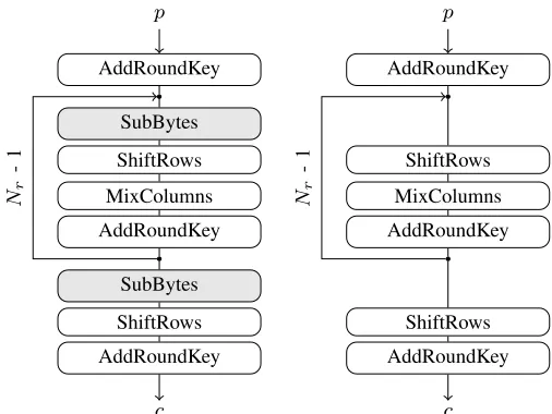
b) SubBytes Layer Manipulation: The SubBytes trans-formation is amongst the most important part of the AES algorithm. It adds non-linearity to the cipher state. We intend to cancel the SubBytes layer as this makes the whole encryption scheme vulnerable to cryptanalysis. The corresponding AES SubBytes manipulation is an extension of the recent work [14]. The manipulation impacts are shortly described for the XTS-AES mode.
The main idea behind the SubBytes modification is to transform the AES into a linear function. Having altered the normal and inverse AES S-box to the identity function, the whole algorithm can be expressed as a linear equation. Hence, we updated all identified S-box and inverse S-box instances in the FPGA bitstream to the identity functionS(x) =x. Due to the linearity of ShiftRowsSR(·)and MixColumnsMC(·), the modified AES (denoted byAESg) can be described as follows:
g
AESk(p) = SR(MC(· · ·MC(SR(p)· · ·)
⊕(ke0⊕ke1⊕ke2⊕...⊕kgNr)
:= MS(p)⊕K.e
The impact of this alteration is illustrated by Fig. 11. The plaintextpis processed by several MixColumns and ShiftRows transformations,Nr−1andNrtimes respectively. This
round-dependent process is denoted by MS(·). The constant Ke
represents the XOR sum of the round keys which have also been preprocessed by certain number of the MixColumns and ShiftRows transformations.
Therefore, with only one known plaintext-ciphertext pair (p, AESgk(p)), the constant Ke can be determined. Thus, all
further phony ciphertexts, that are encrypted by AESgk, can
be decrypted without any knowledge about the actual key. For more detailed information we refer the interested reader to the
p
AddRoundKey
ShiftRows
MixColumns
AddRoundKey
ShiftRows
AddRoundKey
c Nr
-1
p
AddRoundKey
SubBytes
ShiftRows
MixColumns
AddRoundKey
SubBytes
ShiftRows
AddRoundKey
c Nr
-1
Fig. 11: Comparison between AES (left) and modified AES]
(right)
work of Swierczynski et al. [14]. In the following, we extend this approach to the XTS mode.
B. Manipulation Impact for XTS-AES
With the presented AES SubBytes manipulation, an XTS-AES ciphertext can be described as a linear equation too:
c = (AES]k2(i)⊗α
j)⊕AES]
k1((AES]k2(i)⊗α
j)⊕p)
= (MS(i)⊕Kf2)⊗αj⊕MS((MS(i)⊕Kf2)⊗αj⊕p)⊕Kf1
= (MS(i)⊗αj)⊕MS(MS(i)⊗αj)
| {z }
T Wi,j
⊕MS(p)
⊕(Kf2⊗αj)⊕MS(Kf2⊗αj)⊕Kf1
| {z }
CKj
(1)
Note that MS(·)is a linear function, and thus the tweak part
T Wi,j, the plaintext-related part MS(p), and the key-related
part CKj could be separated. Every plaintext pis encrypted
in this way by the FPGA hardware Trojan of our target device.
C. Plaintext Recovery of Encrypted XTS-AES Ciphertexts To recover the plaintexts from the weakly encrypted XTS-AES ciphertexts, the attacker has to obtain two sets of infor-mation:
• 32 plaintext-ciphertext pairs (pi, ci), i ∈ {0, ...,31} of
one sector (512-byte wide), and
• knowledge about the tweak values i and the data unit positionj of the ciphertexts within a sector.
Due to the combination of the data unit’s positionjand the key
k2 (through Galois field multiplication by αj), each position
j in a sector has its own constant key-related part CKj.
Further, CKj is constant for every sector of the memory as
plaintext-ciphertext pairs of one arbitrary sector to generate all
CKj values. To obtain the tweak values T Wi,j, the attacker
needs to obtain the starting value of i identifying the first sector (as explained before, iindicates the sector number and starts from an arbitrary non-negative integer). Generally, this can be achieved through reverse-engineering (ARM code), cf., Section VI.
With this data the attacker can compute the tweak and the key-related parts of Eq. (1). Afterwards, by inverting theMS(·)
function the plaintexts p can be revealed. MS−1(·) can be determined by applying the inverse MixColumns and inverse ShiftRows transformations (dependent on the underlying AES key size).
It is worth mentioning that the produced ciphertext still appears to be random for a victim, who visually inspects the phony ciphertexts from the micro SD card. Therefore, the victim cannot observe any unencrypted data as it would be the case if the FPGA is simply bypassed.
VI. ARMCODE MODIFICATION
In this section we briefly describe the cryptographic self-tests and ARM firmware modifications essential to enable the above presented FPGA hardware Trojan insertion.
A. Utilized Self-tests
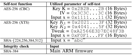
When we reverse-engineered the ARM code using the tool IDA Pro, we were able to identify several functions that check the integrity of the ARM firmware and consistency of several cryptographic functions. Every executed self-test must return a specific integer indicating whether the test passed or not. If any self-test fails, the target device switches to an error state. The corresponding test-vectors used by the self-tests are stored in the SPI flash. Table II provides an overview of all self-tests and the integrity checks. Besides, we also identified
Self-test function Utilized parameter of self-test
AES-256 (CBC) Key K =0x2B2B...2B(16 Bytes) IV =0x3C3C...3C(16 Bytes) Input x =0x1111...11(32 Bytes) AES-256 (XTS) KeyK1=0x2021...3F(32 Bytes) KeyK2=0x4041...5F(32 Bytes) Tweak =0xA2566E3D7EC48F3B Input x =0xF0F1...FF(16 Bytes) SHA-{224,256,384,512} Input x = ”abc”
Integrity check Input
SHA-384 Main ARM firmware
TABLE II: Identified self-tests and firmware integrity check
several relevant security header fields that are processed by the ARM CPU.
The ARM CPU expects to receive a specific signature (during power-up of the system) from the Xilinx FPGA to ensure that it operates correctly after the configuration process. Also, the bitstream length is coded in the header such that the ARM CPU knows the amount of configuration bytes. Lastly, a SHA-384 hash value, calculated over the main ARM firmware, is appended to ensure the program code integrity.
Field Name Offset Byte size Value
Header Signature 0x00 4 0x11223344
FPGA signature 0x04 16 ”SPYRUS_HYDRA2005” Bitstream length 0x14 4 0x45600
SHA-384 hash of2ndimage 0x1D0 48 SHA-384(2ndimage)
TABLE III: Security Header Fields
B. Disabling Self-tests to Modify ARM Code and FPGA Bit-stream
Preliminary tests have shown that even minor code changes, which do not influence the behavior of the firmware, cause the USB flash drive to enter the error state and halt during power-up. It was concluded that there exists an implemented self-test at least checking the integrity of the code. Thus, it became a mandatory prerequisite to find and deactivate such a test. The responsible code was identified due to its obvious structure and function calls.
In addition to the firmware integrity, the correct functionality of several cryptographic algorithms is tested: the AES, ECC and Secure Hash Algorithm (SHA) in the ARM code and the AES inside the FPGA. The individual checks are performed in dedicated functions invoked by the main self-test function, and their corresponding return values are verified. Finally, the self-test succeeds only in case all individual checks are passed. In order to disable the self-test the code was patched in a way that the function always returns zero, which is the integer representation for success. Hence, arbitrary firmware modifications and changes to the cryptographic algorithms can be applied after this patch.
C. Separating Key Derivation and FPGA AES IP-Core As explained in the previous sections, cf., Fig. 8, there is a software AES implementation executed by the ARM CPU and a considerably faster hardware AES instance inside the FPGA. They are both capable of ECB, CBC and XTS operation modes. The software AES is mainly used for self-tests and the hardware AES for key derivation as well as encryption and decryption of the user data stored on the USB flash drive. The key derivation requires the establishment of a secure communication channel between the PC software and the USB flash drive. The FPGA hardware Trojan weakens the AES IP-core making it incompatible to the standard AES, cf., Section V. Thus, the initialization of the communication channel fails and the USB flash drive goes to an error state. To avoid such a situation the firmware has to be changed in such a way that only the original software AES is used during the key derivation and the secure channel establishment (instead of the modified hardware AES inside the FPGA).
are computed by the ARM CPU instead of the FPGA. In total the parameters of 12 AES instance constructor calls have been patched to eliminate the AES dependency between the ARM and FPGA.
D. Recording XTS-AES Parameters
In order to recover all user data from the USB flash drive we need several values for the attack, cf., Section V: 32 plaintext-ciphertext pairs of the same sector, the sector number and the initial tweak value. The latter parameter is hard-coded in the firmware and was obtained by static analysis. The plaintext-ciphertext pairs are acquired at runtime during normal operation of the USB flash drive. In the ARM code there is a highly-speed-optimized function which reads data from the embedded SD card, sends them to the FPGA for decryption and finally copies the plaintexts from the FPGA to the USB endpoint so that the computer receives the requested data. This function was intercepted at several positions in a way that the plaintext-ciphertext pairs and the initial sector number could be obtained. They are then written (only once) in the embedded SPI flash from where they can be read out by an attacker to launch the cryptographic attack.
As explained in Section V, having this information is essential to decrypt the phony ciphertexts due to the underlying XTS mode. We practically verified the plaintext recovery of the weakly encrypted ciphertexts stored on the SD card of our target device.
VII. SUMMARY
In this section we summarize the security problems of our investigated target device and further outline which security barriers might be inserted by the vendor to improve the security of the analyzed USB flash drive.
As previously stated, during our analysis we found a HSM from SPYRUS that is directly connected to the Xilinx FPGA over a single-bit bus. According to [32] it provides certain cryptographic primitives and serves as secure storage device, e.g., for secret (symmetric) keys. We suggest to include the following security measure: during the power-up of the USB flash drive, the FPGA should validate its AES implementation using the AES core provided by the HSM. It should be extremely challenging for an attacker to alter the AES core of the HSM as its internal functionality is realized by an ASIC. The HSM should decide whether the USB flash drive continues (no alteration detected) or switches to an error state (alteration detected).
To further raise the bar for an attacker, the FPGA design should include built-in self-tests for the S-box configuration as well as for the whole AES core. To be more precise, it is recommended to include several test vectors in the FPGA firmware so the FPGA can validate its consistency. Probably, the built-in self-tests do not hinder a more powerful attacker who can disable them, but the reverse-engineering efforts are significantly increased and require a more powerful adversary. Since in our attack scenario we exploited the content of the block RAMs, it is also important to assure its integrity. Their initial content can be encrypted with an appropriate
mode of operation: a built-in circuitry in the FPGA design might (during the FPGA power-up) decrypt the block RAM’s contents and update them with the corresponding decrypted data. By doing so, an attacker cannot replace the highly important S-boxes in a meaningful way, which can have severe security implications as demonstrated in this work.
More importantly, all self-tests (including those we found) should be performed by the HSM. Therefore, the HSM should verify the integrity of the ARM code. Further, the bitstream of the FPGA must be protected (not stored in plain in the SPI flash) and its integrity must be verified e.g., by the HSM. This should prevent any modification attempt on the ARM code as well as on the bitstream, making a firmware modification attack extremely difficult. We should emphasize that an attacker is able to turn the device into a malicious one that can infect the target computer with malicious software, as shown by Nohl et al. [21]. This also highlights the practical relevance of our attack.
VIII. CONCLUSIONS
In this paper we demonstrated the first practical real-world FPGA hardware Trojan insertion into a high-security commer-cial product to weaken the overall system security. We reverse-engineered a third-party FPGA bitstream to a certain extent and replaced parts of the FPGA logic in a meaningful manner on the lowest level. In particular, we significantly weakened the embedded XTS-AES-256 core and successfully canceled its strong cryptographic properties making the whole system vulnerable to cryptanalysis. Our work is a proof of concept that an FPGA can also be one of several weak points of a seemingly protected system. It is important to ensure the integrity of the FPGA firmware as otherwise the system may be compromised by an attacker. This is especially critical in applications where the FPGA acts as master device and where the integrity or confidentiality of the bitstream is not ensured. One can assume that certain determined attackers such as foreign intelligence services are already capable of inserting FPGA backdoors in the presented manner since these kind of attacks do not require a complete bitstream reverse-engineering. Future works must deal with counterfeiting bitstream modification attacks by developing appropriate countermeasures that have to be implemented within an FPGA design.
ACKNOWLEDGMENT
The authors would like to thank Kai Stawikowski and Georg T. Becker for their fruitful comments and help regarding this project.
REFERENCES
[1] SPIEGEL Staff, “Inside TAO: Documents Reveal
Top NSA Hacking Unit,” December 29 2013,
http://www.spiegel.de/international/world/the-nsa-uses-powerful-toolbox-in-effort-to-spy-on-global-networks-a-940969.html.
[2] G. Greenwald, No Place to Hide: Edward Snowden, the NSA and the Surveillance State. Metropolitan Books, 2014.
[4] G. Macri, “Leaked Photos Show NSA Hardware In-terception And Bug-Planting Workstation,” 05 2014, http://dailycaller.com/2014/05/15/leaked-photos-show-nsa-hardware-interception-and-bug-planting-workstation/.
[5] S. T. King, J. Tucek, A. Cozzie, C. Grier, W. Jiang, and Y. Zhou, “Designing and implementing malicious hardware,” in Proceedings of the 1st Usenix Workshop on Large-Scale Exploits and Emergent Threats, ser. LEET’08. Berkeley, CA, USA: USENIX Association, 2008, pp. 5:1–5:8. [Online]. Available: http://dl.acm.org/citation.cfm? id=1387709.1387714
[6] R. Karri, J. Rajendran, and K. Rosenfeld, “Trojan Taxonomy,” in Introduction to Hardware Security and Trust, M. Tehranipoor and C. Wang, Eds. Springer-Verlag, 2012.
[7] S. Narasimhan and S. Bhunia, “Hardware Trojan Detection,” in Introduction to Hardware Security and Trust, M. Tehranipoor and C. Wang, Eds. Springer-Verlag, 2012.
[8] “DataTraveler 5000 FIPS 140-2 Level 2 certification,” 2010. [Online]. Available: http://csrc.nist.gov/groups/STM/cmvp/documents/ 140-1/140crt/140crt1316.pdf
[9] D. McGrath, “Analyst: Altera to catch Xilinx in 2012,” EE Times, Mar. 2011.
[10] S. Drimer, “Security for volatile FPGAs,” Technical Report UCAM-CLTR-763, University of Cambridge, Computer Laboratory, 2009.
[11] E. Rannaud, “From the bitstream to the netlist,” in Proceedings of the´ 16th International ACM/SIGDA Symposium on Field Programmable Gate Arrays, 2008, pp. 264–264.
[12] F. Benz, A. Seffrin, and S. Huss, “Bil: A tool-chain for bitstream reverse-engineering,” in Field Programmable Logic and Applications (FPL), 2012 22nd International Conference on, Aug 2012, pp. 735– 738.
[13] D. Ziener, S. Assmus, and J. Teich, “Identifying fpga ip-cores based on lookup table content analysis,” in Field Programmable Logic and Applications, 2006. FPL ’06. International Conference on, Aug 2006, pp. 1–6.
[14] P. Swierczynski, M. Fyrbiak, P. Koppe, and C. Paar, “FPGA Tro-jans Through Detecting and Weakening of Cryptographic Primitives,” Computer-Aided Design of Integrated Circuits and Systems, IEEE Transactions on, vol. 34, no. 8, pp. 1236–1249, Aug 2015.
[15] R. Chakraborty, I. Saha, A. Palchaudhuri, and G. Naik, “Hardware Tro-jan Insertion by Direct Modification of FPGA Configuration Bitstream,” Design Test, IEEE, vol. 30, no. 2, pp. 45–54, April 2013.
[16] A. C. Aldaya, A. J. C. Sarmiento, S. S´anchez-Solano, “AES T-Box tam-pering attack,” Journal of Cryptographic Engineering, pp. 1–18, 2015. [Online]. Available: http://dx.doi.org/10.1007/s13389-015-0103-4 [17] A. Moradi, D. Oswald, C. Paar, and P. Swierczynski, “Side-channel
Attacks on the Bitstream Encryption Mechanism of Altera Stratix II: Facilitating Black-box Analysis Using Software Reverse-engineering,” in Proceedings of the ACM/SIGDA International Symposium on Field Programmable Gate Arrays, ser. FPGA ’13. New York, NY, USA: ACM, 2013, pp. 91–100.
[18] A. Moradi, A. Barenghi, T. Kasper, and C. Paar, “On the vulnerability of FPGA bitstream encryption against power analysis attacks: extracting keys from Xilinx Virtex-II FPGAs,” in ACM Conference on Computer and Communications Security, 2011, pp. 111–124.
[19] A. Moradi, M. Kasper, and C. Paar, “Black-box side-channel attacks highlight the importance of countermeasures - an analysis of the Xilinx Virtex-4 and Virtex-5 bitstream encryption mechanism,” in The Cryptographers’ Track at the RSA Conference, Feb. 2012, pp. 1–18. [20] “Report of the defense science board task force on high performance
mi-crochip supply,” http://www.acq.osd.mil/dsb/reports/ADA435563.pdf?, 2005.
[21] K. Nohl, S. Kriler, and J. Lell, “BadUSB - On accessories that turn evil,” BlackHat, 2014. [Online]. Available: https://srlabs.de/badusb/ [22] G. T. Becker, F. Regazzoni, C. Paar, and W. P. Burleson, “Stealthy
Dopant-Level Hardware Trojans,” in Cryptographic Hardware and Embedded Systems - CHES 2013 - 15th International Workshop, Santa Barbara, CA, USA, August 20-23, 2013. Proceedings, 2013, pp. 197– 214.
[23] Z. Ding, Q. Wu, Y. Zhang, and L. Zhu, “Deriving an NCD file from an FPGA bitstream: Methodology, architecture and evaluation,” Microprocessors and Microsystems - Embedded Hardware Design, vol. 37, no. 3, pp. 299–312, 2013.
[24] Kingston Technology, “Protect sensitive data with FIPS 140-2 Level 2 validation and 100 per cent privacy.” [Online]. Available: http://www.kingston.com/datasheets/dt5000 en.pdf
[25] “Suite B Cryptography,” 2001. [Online]. Available: https://www.nsa. gov/ia/programs/suiteb cryptography/
[26] “Hex-Rays SA,” http://www.hex-rays.com.
[27] T. Eisenbarth, T. G¨uneysu, C. Paar, A. Sadeghi, D. Schellekens, and M. Wolf, “Reconfigurable trusted computing in hardware,” in Workshop on Scalable Trusted Computing, STC 2007. ACM, 2007, pp. 15–20. [28] J. Daemen and V. Rijmen, “AES Proposal: Rijndael,” in First Advanced Encryption Standard (AES) Conference, Ventura, California, USA, 1998.
[29] D. Canright, “A Very Compact S-Box for AES,” in Cryptographic Hardware and Embedded Systems - CHES, ser. Lecture Notes in Computer Science, vol. 3659. Springer, 2005, pp. 441–455. [30] B. Kakarlapudi and N. Alabur, “FPGA Implementations of S-box vs.
T-box iterative architectures of AES.” [Online]. Available: http://teal. gmu.edu/courses/ECE746/project/reports 2008/AES T-box report.pdf [31] IEEE Std 1619-2007, “IEEE Standard for Cryptographic Protection of
Data on Block-Oriented Storage Devices,” pp. c1–32, 2008.