Proximity Coupled Rectangular Microstrip
Patch Antenna by Varying Thickness
Dinesh B. Ganure1, S. L. Mallikarjun2, P. M. Hadalgi3
Research Student, Dept. of Applied Electronics, Gulbarga University, Kalaburagi, Karnataka, India1
Guest Faculty, Dept. of Applied Electronics, Gulbarga University, Kalaburagi, Karnataka, India2
Professor, Dept. of Applied Electronics, Gulbarga University, Kalaburagi, Karnataka, India3
ABSTRACT: In recent years, the demand for broadband antennas has increased for use in lower frequency and high-speed data communication systems. Printed antennas are economical and easily hidden inside packages, making them well suited for consumer applications. In this study a design has been developed to improve the antenna parameters in terms of impedance bandwidth, gain and radiation properties. The proximity-coupled rectangular microstrip antenna (PRMSA) is proposed. The fabricated antenna uses two-layer substrate with the microstrip-line on the lower layer and the patch antenna on upper layer such as the feed line finishes in an open end underneath the patch. The study is made by comparing thickness of substrate of two layers. By increasing the substrate thickness it is found to be increase in impedance bandwidth and gain. The antenna parameters such as Radiation pattern, reflection coefficient, VSWR and HPBW is calculated and discussed.
KEYWORDS: Rectangular microstrip patch, proximity feed, impedance bandwidth, gain.
I.INTRODUCTION
In the present-time communication, antennas cover a wide range of applications in different areas, such as mobile communication, satellite navigation, internet services, automobiles and radars. Especially they are applied to microstrip antennas, because of its characteristics like low profile, lightweight and low power handling capacity [1-4]. However, gain and bandwidth are sometimes low and not sufficient in most of applications. Modification of shape and using special materials could be useful to solve such backlashes of this type of antennas. WiMAX (Wireless Interoperability for Microwave Access) is one of the latest wireless technologies. This technology can be used in numerous numbers of applications: the broadband services such as Voice over IP (VOIP), portable mobile connectivity, Digital Subscriber Line (DSL), etc [5].
The basically a microstrip antenna consists of a planar radiating structure of desired geometrical shape on one side of a dielectric substrate and a ground plane on the other. Commonly used microstrip radiating geometries are rectangular and circular [6]. However, other shapes are also considered depending upon the application.
To couple power to a microstrip antenna is as important as the selection of a suitable geometry for a particular application. A variety of feeding mechanisms are available and some important among them are Microstrip feed, Co-axial feed, Aperture coupling feed and Proximity coupling feed. The Proximity coupling feed technique is used for the proposed microstrip antenna. It uses a two –layer substrate with the microstrip line on the lower layer and the patch antenna on the upper layer. The feed line terminates in an open end underneath the patch [6].
II.ANTENNA DESIGN
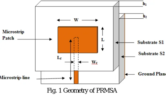
Figure 1 shows the top view geometry of PRMSA. The PRMSA consists of a length L and width W is etched on top surface of substrate S1. The microstripline feed of length Lf and width Wf is etched on the top surface of substrate S2. The substrate S2 is placed below substrate S1 and the bottom surface of the substrate S2 acts as the ground plane
.
Fig. 1 Geometry of PRMSA
The PRMSA has been designed for 3 GHz. The physical dimension of rectangular radiating patch and feedline are approximately determined from equations [1] and is shown in the Table 1.
Table 1 Designed parameters of proposed antennas
Antenna Geometry
Parameters Dimensions
Length of the patch, L 24.25mm
Width of the patch, W 31.00mm
Length of feedline, Lf 12.72mm
Width of feedline, Wf 1.58mm
Thickness of the substrate S1 = 1.6mm & S2 = 0.8mm
III. EXPERIMENTAL RESULTS AND DISCUSSION
The measurements are taken on Vector Network Analyzer (Rohde & Schwarz, German make ZVK Model No. 1127.8651). The impedance bandwidths over return loss less than -10dB for the proposed antennas are measured. The variation of return loss versus frequency of PRMSA with different thickness of substrates such as S1 = 0.8 mm & S2 = 0.8 mm and substrate S1 = 1.6 mm & S2 = 0.8 mm by keeping the same permittivity which is shown in Fig. 2. The experimental impedance bandwidth is defined as,
Impedance Bandwidth (%) = × 100 ... (1)
Fig. 2 Variation of Return loss Vs Frequency of PRMSA
From the figure it is observed that, PRMSAwith Substrate height, (S1 = 0.8 mm & S2 = 0.8 mm operates at 2.88 GHz. The experimental impedance bandwidth (BW) is found to be 40 MHz (1.38%). The minimum return loss measured in this antenna is -13.86 dB. Similarly, the antenna with Substrate height (S1 = 1.6 mm & S2 = 0.8 mm operates at 2.82 GHz and impedance bandwidth (BW2) is found to be 80 MHz (2.83%), which is 2.05 times more when compared with the antenna with Substrate height (S1 = 0.8 mm & S2 = 0.8mm). Also, the minimum return loss measured in this antenna is -14.42 dB.
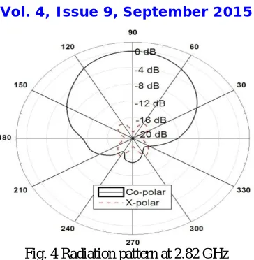
The X-Y plane co-polar and cross-polar radiation patterns of PRSMA with different thickness are measured at their resonating frequencies and are shown in Figures 3 & 4. These figures indicate that the antennas show broader side radiation characteristics. The crosspolarization levels of these antennas are found to be minimum which is below -10dB and -16dB for respective antennas as shown.
Fig. 4 Radiation pattern at 2.82 GHz
The half power beam width (HPBW) and gain for the proposed antennas is calculated for their resonating frequencies and are also shown in Table 2.
The gain of proposed antenna is calculated using absolute gain method given by the equation, [6]
( ) = − ( ) − …… (2)
Where, Pt and Pr are transmitted and received powers respectively, Gt is the gain of the pyramidal horn antenna and R is the distance between transmitting antenna and antenna under test. The gain of the antenna is tabulated in Table 2
.
Table 2 Calculated Min.crosspolar, Gain, HPBW and VSWR
Substrate Height Freq. in GHz Min. Cross polar in dB
Gain in dB HPBW in degrees VSWR S1=0.8mm
S2=0.8mm 2.88 -10 6.61 86
0
1.41
S1=1.6mm
S2=0.8mm 2.82 -16 14.61 83
0
1.47
The antenna with S1=1.6mm & S2=0.8mm showsthe input impedance has a loop at the center of Smith chart which illustrates the matching of the feedline and radiating patch at 50Ω [7] which is shown in Figure 5.
Fig. 5 Smith chart profile
0 0.2 0.5 1 2 5 10
-5 -2 -1 -0.5 0.5 1 2 5
CH1 1 U
FIL 1k 1k FIL 1k 1k CAI
START 2.5 GHz STOP3.5 GHz
S11
1
1: 56.08 j28.56
2.845 GHz
IV.CONCLUSION
The complete experimental study illustrates that the antennas are relatively simple in design and fabrication and quite good in enhancing the bandwidth and give better broadside radiation pattern at the resonating frequencies also the gain is found to be increased as the thickness of antenna is increased. These antennas are also better as they use low cost substrate material and find the applications in S-band frequency range such as in modern wireless communication systems.
REFERENCES
[1] I. J. Bahl and P. Bhartia, Microstrip Antennas, Artech House, Dedham, MA, 1980.
[2] Fan Yang; Xue-Xia Zhang; Xiaoning Ye; and Yahya Rahmat-Samii, “Wide-Band E-Shaped Patch Antennas for Wireless Communications”, IEEE Trans. Antennas Propog. Vol. 49, No. 7, 2001.
[3] Girish Kumar and K. P. Ray, Broadband Microstrip Antennas, Norwood, MA: Artech House, 2003. [4] David M. Pozar, Microwave Engineering, Addison Wesley Publishing Company, Inc. 1990.
[5] Yahya Entiefa Mansour, Single slot dual band microstrip antenna for WiMAX application, Atilim University, June 2014. [6] Ramesh Garg, Microstrip antenna design handbook, Artech House, Noorwood, MA, 2001.
S. L. Mallikarjun and P. M. Hadalgi, “Single layer modified rectangular microstrip array antenna for multi band and wide band applications”, Indian Journal of Radio Physics, Vol. 39, pp.156-162, June 2010.
BIOGRAPHY
Mr. Dinesh B Ganure received his M.Sc., M.Phil degree in Applied Electronics from Gulbarga University, Gulbarga in the year 2010, 2013 respectively. He is working as a Research Scholar in Dept. of Applied Electronics, Gulbarga University, Gulbarga. He is an active researcher in the field of Microwave Electronics.
Dr. S.L. Mallikarjun received his M.Sc., M.Phil. and Ph.D. degree in Applied Electronics from Gulbarga University, Gulbarga in the year 2005, 2007 and 2011 respectively. He is working in Dept. of Applied Electronics, Gulbarga University, Gulbarga. He is an active researcher in the field of Microwave Electronics. His area of interest includes microstrip antenna, arrays and dielectric resonator antenna. He has more than 70 publications in reputed International/National Journals and in conference and symposia.