Topological Issues Related to Single-Phase
Power Factor Correction
Gavish Gothria1, Abhishek Gupta1,Anuj Singh1 Dronacharya College Of Engineering,Gurgaon,India
Abstract-
The equipment connected to an electricity distribution network usually needs some kind of power conditioning, typically rectification, which produces a nonsinusoidal line current due to thenonlinear input characteristic. With the steadily increasing use of such equipment, line current harmonics have become a significant problem. Their adverse effects on the power system are well recognized. They include increased magnitudes of neutral currents in three-phase systems, overheating in transformers and induction motors. Several international standards now exist, which limit the harmonic content due to linecurrents of equipment connected to Electricity distribution networks. As a result, there is the need for a reduction in line current harmonics, or Power Factor Correction - PFC.
1. INTRODUCTION
1.1 Nonlinear loads and their effect on the electricity distribution network
The most significant examples of nonlinear loads are reviewed next ,Single-phase diode rectifiers are needed in relatively low power equipment that need some kind of power conditioning, such as electronic equipment
(e.g. TVs, office equipment, battery
chargers, electronic ballasts) and household appliances. For higher power, three phase diode rectifiers are used, e.g. in variable-speed drives and industrial equipment. In both single- and three-phase rectifiers, a large filtering capacitor is connected across the rectifier output to obtain DC output voltage with low ripple. As a consequence, the line current is nonsinusoidal. As an example, a single-phase diode rectifier is presented in Fig. 1.1,
together with its line current and voltage waveforms. The odd harmonics of the line current, normalized to the fundamental, are shown in the same figure. The normalized amplitudes of the 3rd, 5th, 7th and 9th harmonics are significant.
While the effect of a single low power nonlinear load on the network can be considered negligible, the cumulative effect of several nonlinear loads is important.These effects include:
Losses and overheating in transformers, shunt capacitors, power cables leading to premature aging and failure.
Reduced power factor, hence less active power available from a wall outlet having a certain apparent power rating.
Distortion of the line voltage via the line impedance, as shown in Fig. 1.1, where
the typicalworst-case values,
Telephone interference.
Errors in metering equipment.
Increased audio noise.
Fig. 1.1 Single-phase diode bridge rectifier: a) Schematic; b) Typical line current and voltage waveforms; c) Odd line current harmonics normalized to the fundamental.
II. STANDARD REGULATING LINE CURRENT HARMONICS
The previously mentioned negative effects of line current distortion have prompted a need for setting limits for the line current harmonics of equipment connected to the electricity distribution network.
Standardization activities in this area have been carried out for many years. Items of electrical equipment are categorized into four classes (A, B, C and D),for which specific limits are set for the harmonic content of the line current.
Class A includes: balanced three-phase
equipment; household appliances,
excluding equipment identified as Class D; tools, excluding portable tools; dimmers
for incandescent lamps and audio
equipment. Equipment not specified in one of the other three classes should be
considered as Class A equipment. The limits for Class A are presented in Table 1.1.
Class B equipment includes: portable tools; and nonprofessional arc welding equipment. Thelimits for this class are those shown in Table 1.1, multiplied by a factor of 1.5.
Class C includes lighting equipment. For an active input power greater than 25W, the harmonic currents should not exceed the limits presented in Table 1.2
Class D are presented in Table 1.3. They are defined in both powerrelated and absolute terms. Initially, Class D included equipment having an active input power less than or equal to 600W, and an input current waveform – normalized to its peak value, Ipk – which stays within the envelope shown in Fig. 1.2 for at least 95% of the duration of each half-period, assuming that the peak of the line current waveform coincides with the center line.
Fig. 1.2 Envelope of the input current used to classify Class D equipment, as defined in the first edition ofIEC 1000-3-2.
Table 1.2 Limits for Class C equipment in standard IEC 1000-3-2.
Table 1.3 Limits for Class D equipment in standard IEC 1000-3-2.
III. METHODS FOR IMROVING EFFICIENCY
The PFC stage performs an additional power processing operation, and therefore it has a negative impact on the overall efficiency of the power supply. In this dissertation, we aim at improving its efficiency by reducing the switch conduction losses in the combined diode bridge and PFC stage, as well as on circuit techniques for reducing the switching losses.
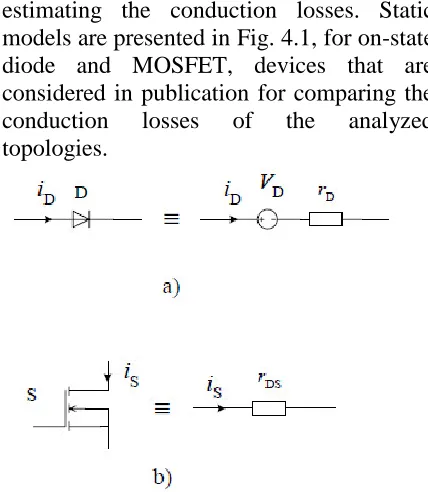
IV. REDUCTION OF CONDUCTION LOSSES
Conduction losses are caused by the current flowing through a non-ideal switching device in the on state, which determines a certain voltage drop on the device. A static model of the switching device is useful for
estimating the conduction losses. Static models are presented in Fig. 4.1, for on-state diode and MOSFET, devices that are considered in publication for comparing the
conduction losses of the analyzed
topologies.
Fig. 4.1 Static models for an on-state switching device: a) Diode; b) MOSFET
As shown in Fig. 4.1, the static characteristic of the on-state diode can be modeled as a voltage source VD in series with a resistor rD . On the other hand, the appropriate static model for the on-state MOSFET is just a resistor rDS . With these models, it is straightforward to calculate the conduction losses of diode D:
whereID, av and ID, rms are the average and RMS diode currents, respectively. Similarly,
the conduction losses of switch S
(MOSFET) are expressed as:
of the switches. Considering also (4.1) and (4.2), we can conclude that one way to diminish the total conduction losses is to reduce the number of switches that are in the
power path and/or to reduce the
average/RMS currents flowing through the
switches, assuming that the rDS of
MOSFETs and the VD and rD of diodes remain unchanged. As a result, switches with higher voltage rating and therefore with higher losses need to be used
V. REDUCTION OF SWITCHING LOSSES
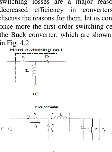
The commutation process of real switching devices takes a certain time, during which the instantaneous power dissipated in the device can be very large. Therefore, switching losses are a major reason for decreased efficiency in converters. To discuss the reasons for them, let us consider once more the first-order switching cell and the Buck converter, which are shown again in Fig. 4.2.
Fig. 4.2 a) Hard-switching cell; b) Buck converter.
The switching cell is labeled „hard-switching cell‟, because there is no
mechanism in place to decreasethe
switching losses. The inductor current I isassumed to be constant, fact which
givesspecific characteristics to the switching mechanism. In addition, the switching mechanism depends for certain aspects on the types of switching devices that are used.
VI. CONCLUSION
We first analyzed the requirements for the EMI filter of a PFC stage based on a Boost converter operating in DICM. As expected, the differential-mode conducted EMI is larger in DICM when compared to CICM, when constant switching-frequency is used and for the same power level, which supports our motivation to investigate higher-order topologies. It was also shown that for both the constant and the variable
switching-frequency cases, the input
impedance of the converter is practically purely resistive and no instabilities can arise from the interaction with the EMI filter.
Finally, we concentrated on reducing the switching losses by using ZVS and we proposed a novel ZVT Buck converter. We then applied the proposed technique to a
500W forward converter, for which
simulations show an efficiency improvement approximately from 2% at light load to 5.5% at full load. Even if the technique is presented for DC/DC applications, its
versatility allows the application to
REFERENCE
[1] J. Cho, J. Baek, D. Yoo, H. Lee, “Reduced conduction loss zero-voltage-transition power factor correction converter with low cost”, IEEE Trans. on Industrial Electronics, vol. 45, no. 3, pp. 395-400, June 1998.
[2]R. D. Middlebrook, “Coupled-inductor and other extensions of a new optimum topology switching DC-to-DC converter”, in Proc. of IEEE Industry Applications Society Annual Meeting, 1977. Reprinted in Advances in switched-mode power conversion, Vol. I&II, pp. 331-347. Pasadena, CA, USA, TESLAco, 1983. [3] M. C. Ghanem, K. Al-Haddad, G. Roy, “A new single phase buck-boost converter with unity power factor”, in Conference Record of the 1993 IEEE Industry Applications Society Annual Meeting, IAS’93, pp. 785-792, 1993.
[4]J. S. Glaser, A. F. Witulski, “Design issues for high power factor AC-DC converter systems”, in Proc. of IEEE Power Electronics Specialists Conference, PESC’95, pp. 542-548, 1995.
[5] V. Grigore, J. Kyyrä, “A new zero-voltage-transition PWM switching cell”, in Proc. of
the 1997 Finnish Workshop on Power and Industrial Electronics, FINPIE/97, pp. 79-84,