An Efficient SBST Scheme for
Multiple-Memory based Multi-Processor Circuits
RajanaK.V1, Anjali Brite2
PG Student, Dept. of Electronics and Communication Engineering, Nehru College of Engineering andResearch Centre,
Thrissur, India1
Assistant Professor, Dept. of Electronics and Communication Engineering, Nehru College of Engineering and Research
Centre, Thrissur, India2
ABSTRACT: To reduce the performance stemming caused due to the execution of branch instructions in pipelined architecture, BPU architectures play a very important role. Mainly BPU has got two mechanisms, BHT and BTB. In this paper a new mechanism which is a combined form of both is described and testing of this BPU memory is another constraint. The conventional method used to test the BPU memory was hardware testing scheme known as built-in self-test (BIST). In order to overcome the disadvantages of BIST software based self-testing scheme was developed, software based self-testing (SBST), where a separate entity is not required while testing a module. In this paper a new genetic algorithm is introduced as an efficient SBST scheme for testing BPU memory to make the complete system more efficient by reducing the redundancy of test patterns to the maximum extent by using various evolutionary strategies. A comparative study followed by a complete optimisation in terms of area, power and delay between the three architectures are done and in order to make it application specific the existing as well as the proposed systems are then implemented on a multiple memory based multiprocessor circuit. The very high speed IC hardware description language (VHDL) model of the complete system is simulated using the most efficient professional fault simulator ModelSim SE 6.2b.Also for the synthesis and analysis of HDL designs, for timing analysis and to obtain the design summary of various modules XILINX ISE 13.2 is used. Also the hardware implementation of the system is done using MATLAB and SPARTAN 6 FPGA kit.
KEYWORDS:testing, multiprocessor, built-in self-test, software based self-test, genetic algorithm, evolutionary strategies, branch history table, branch target buffer, branch prediction unit, very high speed IC hardware description language.
I.INTRODUCTION
same by adding more test quality at a low cost. To make it application specific the whole system is implemented using a multiple memory based multiprocessor circuit. The main key problem regarding pipelining is branches.
Now consider a code sequences, If ( p>10) {
q = r; } else { q = s; }
This compiles into something like Cmp p, 10; p>10?
b1e L1
movr,q; q=r br L2
L1: movs,q; q=s L2:- - - -
By the time the conditional branch at line 2 reaches the execute stage in the pipeline, the processor must have already fetched and decoded the next couple of instructions. But the processor may be ambiguous about which instruction should it fetch and decode, either to fetch and decode the if branch (lines 3, 4) or else branch (line 5)? It won’t really know until the conditional branch gets to the execute stage, but in the case of deeply pipelined processor that might be several cycles away and it can’t afford to just wait. For every six instructions on average the processor encounters a branch, and if it was to wait several cycles at every branch then most of the performance gained by using pipelining in the first phase would be lost. Here is the importance for a BPU. The branch predictor attempts to avoid the waste of time by trying to guess whether the conditional jump is most likely to be taken/not taken
II. RELATED WORKS
III.SYSTEM MODEL
The existing system is all about a branch prediction module (BHT, BTB) design. And the testing of BPU memory which is embedded inside a processor using software based testing scheme SBST, and also the conventional testing scheme which is hardware based known as built-in self-test (BIST).
3.1. Branch History Table
A BHT is based on a data structure which stores the result (Taken or Not Taken) of previously executed conditional branches. The goal of a BHT is simply to forecast whether a given conditional branch result will be taken or not. The BHT is accessed during the Decode stage each time the instruction processed by the stage is a conditional branch.
Fig.1BHT Module
This BHT is designed using a Look-Up Table LUT) that is nothing but an 8 bit ROM of size 256, an 8 bit state machine which acts like a decision block with input equals the output from ROM as shown in figure 1. The decision block checks the LSB of input and accordingly it releases the output value, checking the first 2 MSB bits of this output it is possible to predict whether the test pattern are taken or not taken. If the 2 bit MSB is “10” it is predicted as not taken and “01” means taken. The rest of the bits of the output resemble the LSB values of input. The output from LUT which is fed as input to the decision block is nothing but the output from 8 bit LFSR which is equal to the value which is stored in the RAM for the corresponding address. In order to check the redundancy of test pattern it’s necessary to compare the output from the LUT as well as the output from decision block using an XOR gate, which is fed back to the LUT. Since it checks only few test patterns and also creates redundancy BHT based BPU mechanism came.
3.2. Branch Target Buffer
The BTB adopts a more aggressive approach to branch prediction, just by checking the target address it will come to know whether the data has been previously executed or not. Moreover the instructions are accessed during the fetch stage itself. For this design an 8-bit linear feedback shift registers (LFSR), An 8-bit RAM of size 256, where the output
from this LFSR is fed as input address to RAM. The output from the 8 bit LFSR is fed as one of the input to the XOR
Fig.2BTB Module
3.3 BIST
Built-in self-test is one of the conventional testing scheme. If BIST is used to test a module it is necessary to add a separate entity while doing the test since it is purely hardware based. The figure 3 shows built-in self-test (BIST) block diagram. The de-bouncer actually consists of 6 inputs and outputs respectively. When a switch is being pressed and hold during that particular time it reads many value, so in order to take a single value as the output it is used. By giving the one of the switch output value of de-bouncer and a reset value as inputs the teller produces an output which in turn fed as one of the input to multiplexer, the output is nothing but from the LFSR output. Using one of the switch output as select line one of the input value will get switched
Fig.3BIST Module
to the output. The complete lower blocks are for the generation of seed value for the BIST. The output from de multiplexer is fed as input to the BIST. The BIST consists of mainly two blocks: -LFSR, SIRS. From this block the error value after testing is received. It has got many disadvantages like high area overhead, increased power consumption also due to large signal routing paths.
3.4. SBST
while testing a module. Actually a small separate code can be used for SBST implementation and it is then embedded into the main program module for testing the memory. Normally the memory testing using SBST consists of two process states. By giving clock, idle=0 it acts like a normal RAM, during the second process states by giving second clock tclk, idle=1 it starts testing the memory and give the error value as well as non-redundant test patterns as the output.
IV.PROPOSED SYSTEM
4.1. Combined architecture
Since the single architectures of BPU have got their own disadvantages, it is essential to find out a new mechanism which combines all the advantages of BHT, BTB as well averages the demerits of both. The redundancy of final test patterns is negligible when compared to single architecture. Also testing of all the test patterns are carried out consuming very less time with maximum efficiency.
Fig. 4 combined architecture
In figure 4, the block diagram of combined architecture of BPU is shown. It consists of both single architecture modules BHT, BTB. The outputs obtained from both are sorted to obtain non-redundant test patterns and fed as data input to the RAM_SBST module which in turn used for the testing of the memory.
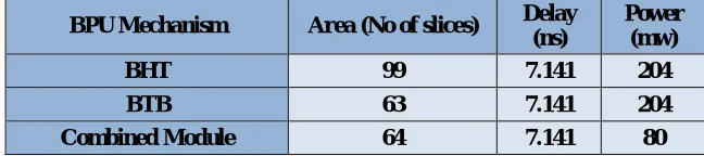
4.1.1. Comparative study of BPU mechanisms
The combined module is actually a combination of advantages of both BTB, BHT. Even though the time consumption of all the three mechanisms are comparable it consumes only very few power compared to other two and area compared to BHT is Also very less. The Table 1 shows the comparative study of all the three BPU mechanisms in terms of area, power and delay.
BPU Mechanism Area (No of slices) Delay
(ns)
Power (mw)
BHT 99 7.141 204
BTB 63 7.141 204
Combined Module 64 7.141 80
Table 1Study of BPU mechanisms
4.2. Genetic Algorithm
continuously. And according to the proximity each test patterns from the main LUT is subdivided and stored into small eight groups each having the same proximity. In order to avoid the redundancy further and also to make the SBST testing scheme more efficient, each test patterns from the main LUT is checked with those test patterns which are stored inside eight LUTs and if it shows any resemblance one of the value from the respective group is taken as output value only for once.
4.3. Comparative Study
Fig.5 Design Summary of Genetic Algorithm
After doing the comparative study with the conventional testing scheme (BIST), existing method (SBST), it is more efficient to use genetic algorithm to test the memory inside the processors. Complete optimisation is obtained in terms of area, power and delay. The area utilisation in terms of number of LUTs, slices are very less for genetic algorithm compared to other two schemes shown in figure 5
Fig.6Timing Report of Genetic Algorithm
Fig.7 Power Analysis of Genetic Algorithm
The table 2 shows the comparative study of all the three testing mechanisms in terms of area, power and delay. It is clear that the area as well as power consumption is comparatively very less for the proposed system and also the delay is less even though it doesn’t make much difference when compared to others.
Testing schemes Area Delay Power
(No of slices) (ns) (mw)
BIST 104 8.015 205
SBST 64 7.141 80
Genetic Algorithm 50 6.098 51
Table 2 Study of Testing Schemes
4.4. Application
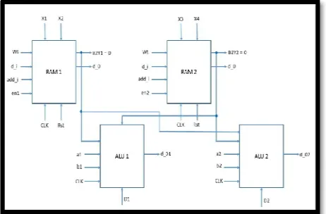
The multiple memory based multi-processor platform can be used for the implementation of existing as well as proposed system. Here a simple ALU can perform the role of this multiprocessor by designing two ALU’s, two Ram’s. A single ALU can access both the memories at a time but the other ALU can only access the memories after checking the select lines x1, x2, x3, x4 as well as the value of the variable BZY1, BZY2 as shown in figure 8.
The existing system, SBST can be implemented by taking the first sequence from final output which is then fed as one of the input to the ALU and taking the second sequence which in turn acts as the second input of ALU. Since the select line of ALU is half the number of bits of SBST output test patterns, only the 4 bits from LSB of the third sequence is fed as select line to the ALU.At the same time the proposed system, genetic algorithm can also be implemented using multiple memory based multiprocessor. One of the outputs from the genetic algorithm is fed as one of the input to the ALU. Since the ALU consists of two inputs the other one is kept as a constant, and here it is five. And the outputs are stored accordingly to the output variable of ALU.
V.SIMULATION RESULTS
The hardware is modelled using VHDL coding. Simulation results are verified in Model Sim 6.2b. and it is synthesized and implemented in Xilinx ISE 13.2, using SPARTAN 3E. The output waveforms of BHT is shown in figure 9 in which the outputs y3 from LUT and outtemp2 from decision block are fed as input to XOR and the final output outtemp3 gives the non-redundant test patterns.
Fig.9 Output waveform of BHT
The figure 10 shows the output waveform of BTB y, y1 acts as the two inputs of XOR module and the output from the same is y2 which is fed as the input address to the RAM module. According to the value of we the output is decided, whether to switch the output to d_o or to y.
Fig.10 Output waveform of BTB
Fig.11output waveform of BIST
The output waveform of combined architecture is shown in figure 12.The two outputs outtemp,out1 gives the maximum non redundant testpatterns compared to single architecture as well as error value after testing the memory.The value of d_i is the XOR’ed output of both BHT,BTB which is then fed as input to the main module.
Fig.12 Output waveform of combined architecture
The figure 13 above shows the output waveform of genetic algorithm.lut0 to lut7 shows the 8 subgroups of main lut(lutstd).The dataout shows the selection of subgroup done with reference to the main lut which is grouped according to te proximity between lutstd,lfsr.
Fig.13 Output waveform of Genetic
Fig.14 Implementation of SBST
The implementation of genetic algorithm is shown in figure 15 below .The output of genetic algorithm is fed from testt to ALU,one of the input of ALU and the other one is noting but a constant value “00000101.cout is the final output.
Fig.15 Implementation of Genetic Algorithm
VI. HARDWARE IMPLEMENTATION
Fig.16 Hardware implementation
VII.CONCLUSION
VLSI design of an efficient BPU mechanism is proposed for hybrid or superscalar architectures. Designed the combined architecture of BPU which includes both BHT, BTB using VHDL coding. Thus the performance stemming can be reduced to maximum in a super scalar architecture eliminating the drawbacks of single architecture of BPU. Also a comparative study between all the three BPU mechanisms is done. And the main focus is given to the new genetic algorithm and the comparative study with other two testing schemes (BIST, SBST) in terms of area, power, and delay. By using this algorithm, it is possible to cover maximum number of test patterns with negligible redundancy and with very less power as well as area. The existing systems as well as the proposed systems are also implemented using multiple-memory based multi-processor. Simulated in Model SIM 6.2b and synthesized using Xilinx ISE 13.2.The hardware implementation can be done using the software MATLAB 9.1 and SPARTAN 6 FPGA kit
.
REFERENCES
[1] Ernesto Sanchez, “On the Functional Test of Branch Prediction Units”, IEEE transactions, vol.2, no.6, June 2014, pp.1-14.
[2] Michael A. Skitsas,” Toward Efficient Check-Pointing and Rollback under On-Demand SBST in Chip Multi-Processors”, IEEE 21st International On-Line Testing Symposium (IOLTS), vol 22, no.3, July 2015, pp.110-115.
[3] Alpanasingh,”BIST-built in self test A Testing Technique”, international journal, vol.2, no.2, 2014, pp.83-88.
[4] Georgios Theodorou,”Software-Based Self-Test for Small Caches in Microprocessors” IEEE transactions, vol.33, no. 12, December 2014, PP.1991-2004.
[5] P. Bernardi,”On-Line Software-Based Self-Test of the Address Calculation Unit in RISC Processors“, 17th IEEE European Test Symposium (ETS), vol.22, no.4, June 2012, pp.87-99.
[6] M. SonzaReorda,”On the Functional Test of Branch Prediction Units based on Branch History Table”, IEEE/IFIP 19th International Conference on VLSI and System-on-Chip, vol.33, no. 3, October 2011, PP. 278-283.
[7]N.Foutris,”MT-SBST: Self-Test Optimization in Multithreaded Multicore Architectures”, IEEE International Test Conference, vol.10, no.3, April 2011, pp.1-10.
[8]M.Hatzimihail,” A Methodology for Detecting Performance Faults in Microprocessors via Performance Monitoring Hardware”, IEEE International Test Conference, vol.14, no.1, November 2011, pp.1-10.
[9] D. Sorin, M. Martin, “Safety net: improving the availability of shared memory multiprocessors with global checkpoint/Recovery”, 29th Annual International Symposium, vol.13, no.2, 2002, pp. 123–134.
[10] O. Khan and S. Kundu, “Hardware/software co design architecture for online testing in chip multiprocessors “, IEEE Transactions, vol. 8, no. 5, sept-oct. 2011, pp. 714 –727.