Implementation and Evaluation of One-Time Programs
(Full Version)
?Kimmo J¨arvinen1, Vladimir Kolesnikov2, Ahmad-Reza Sadeghi3, and Thomas Schneider3
1
Dep. of Information and Comp. Science, Aalto University, Finland
2 Alcatel-Lucent Bell Laboratories, Murray Hill, NJ 07974, USA
3
Horst G¨ortz Institute for IT-Security, Ruhr-University Bochum, Germany {ahmad.sadeghi,thomas.schneider}@trust.rub.de? ? ?
Abstract. The power of side-channel leakage attacks on cryptographic implementations is evident. Today’s practical defenses are typically attack-specific countermeasures against certain classes of side-channel attacks. The demand for a more general solution has given rise to the recent theoretical research that aims to build provably leakage-resilient cryptography. This direction is, however, very new and still largely lacks practitioners’ evaluation with regard to both efficiency and practical security. A recent approach, One-Time Programs (OTPs), proposes using Yao’s Garbled Circuit (GC) and very simple tamper-proof hardware to securely implement oblivious transfer, to guarantee leakage resilience.
Our main contributions are (i) a generic architecture for using GC/OTP modularly, and (ii) hardware implementation and efficiency analysis of GC/OTP evaluation. We implemented two FPGA-based prototypes: a system-on-a-programmable-chip with access to hardware crypto accelerator (suitable for smartcards and future smartphones), and a stand-alone hard-ware implementation (suitable for ASIC design). We chose AES as a representative complex function for implementation and measurements. As a result of this work, we are able to under-stand, evaluate and improve the practicality of employing GC/OTP as a leakage-resistance approach. Last, but not least, we believe that our work contributes to bringing together the results of both theoretical and practical communities.
Keywords: Garbled Circuit, Hardware Implementation, Leakage-Resilience, One-Time Pro-grams, Secure Function Evaluation
1
Introduction
Side-channels and protection. For over a decade, we saw the power and elegance of side-channel attacks on a variety of cryptographic implementations and devices. These attacks refute the assumption of “black-box” execution of cryptographic algorithms, allow the adversary to obtain (unintended) internal state information, such as secret keys, and consequently cause catastrophic failures of the systems. Often the attacks are on the device in attacker’s possession, and exploit physical side-channels such as observing power consumption [22], emitted radiation [9, 42, 1], and even the memory cache [21, 37, 35]. Moreover, even when no computation is performed, stored secrets may be leaked [46] or read out from RAM, which is typically not erased at power-off, allowing, e.g., cold-boot attacks [16]. Hence, from the hardware perspective, security has been viewed as more than the algorithmic soundness in the black-box execution model (see, e.g., [28, 59, 57, 48]).
Today’s practical countermeasures typically address known vulnerabilities, and thus target not all, but specific classes of side-channel attacks. The desire for a complete solution motivated the recent burst of theoretical research inleakage-resilient cryptography, the area that aims to define security models and frameworks that capture leakage aspects of computation or/and memory.
?
A short version of this paper appears in CHES 2010 [20].
??
Supported by EU FP7 project CACE.
? ? ?
Information leakage is typically modeled by allowing the adversary learn (partial) memory or execution states. The exact information given to the adversary is specified by the (adversarily chosen) leakage function. Then, the assumption on the function (today, usually the bound on the output length) directly translates into a physical assumption on the underlying device and the adversary. Proving security against such an adversary implies security in the real-world with the real device, subject to corresponding assumption (see [39] for a survey on this strand of research). We note that many of the results of this new line of research (i.e., leakage assumptions and leakage-resilient constructions), although clearly stated, have not yet been evaluated by practitioners and side-channel community.4 Further, efficiency is a major concern with today’s solutions, since, e.g., embedded systems on an integrated circuit (IC) have very little cost tolerance.5
Secure Function Evaluation in hardware and leakage-resilience.Efficient Secure Func-tion EvaluaFunc-tion (SFE) in an untrusted environment is a longstanding objective of modern cryp-tography. Informally, the goal of two-party SFE is to let two mutually mistrusting (polynomially-bounded) parties compute an arbitrary function on their private inputs without revealing any information about the inputs, beyond the output of the function. SFE has a variety of applica-tions, particularly in settings with strong security and privacy demands. Deployment of SFE was very limited and believed expensive until recent improvements in algorithms, code generation, computing platforms and networks.
As advocated in numerous prior works [31, 30, 26, 40, 25, 19, 24], Garbled Circuit (GC) [60] is often the most efficient (and thus viable) SFE technique in the two-party setting. As we argue in §3.2, the emerging fully homomorphic encryption schemes [11, 7, 47] are unlikely to approach the efficiency of GC.
Because of the execution flow of the GC solution (one party can non-interactively evaluate the function once the inputs have been fixed), the security guarantees of SFE are well-suited to prevent allside-channel leakage. Indeed, even GC evaluation in the open reveals no information other than the output. Clearly, it is safe to let the adversary see (as it turns out, even to modify) the entire GC evaluation process. The inputs-related stage of GC can also be made non-interactive with appropri-ate hardware such as Trusted Platform Modules (TPM) [15]. Goldwasser et al. [13] observed that very simple hardware is sufficient, one that, hopefully, can be manufactured tamper-resistant at low cost. They propose to use One-Time Programs (OTP), a combination of GC and above hardware, for leakage-resilient computation. The combination of non-interactive computation, count-limited execution, and leakage resistance holds great promise, e.g., for outsourcing computation and soft-ware business model. As we explain below one of our goals in this paper is to evaluate today’s performance of OTP in hardware. Indeed, one of our goals is to evaluate today’s performance of OTP in hardware.
Our objectives.Practical efficiency of SFE and leakage-resilient computing is critical. Indeed, in most settings, the technology can only be adopted if its cost impact is acceptably low. In this work, we pursue the following two objectives.
First, we aim to mark this (practical efficiency) boundary by consideringhardware-accelerated GC evaluation. In our implementation, we use state-of-the-art GC techniques, and optimize the code for embedded systems such as Systems on a Chip (SoC) based on FPGAs. Hash functions form the most significant computational burden in GC evaluation and throughout this paper we use SHA-256 as hash function. A cost-effective, straightforward and useful accelerator architecture is likely to implement SHA-256 functions in hardware, and thus will have similar cost structure to what we consider: low-cost SHA-256 evaluation and high-cost memory access. Implementing (at least some of) the SFE functionality in hardware promises to significantly improve computation speed and reduce power consumption. Our optimized hardware design and implementation allows us to evaluate costs, benefits and trade-offs of hardware support for GC evaluation.
Second, we use our GC hardware-accelerator to implement OTP and evaluate the efficiency of this provably leakage-resilient protection. The envisioned applications for OTPs mentioned in [13] are complex functionalities such as one-time proofs, E-cash, or extreme software protection (with features such as limited number of executions or temporary transfer of cryptographic abilities).
4
Indeed, ongoing work of [49] investigates the practical applicability and usability of theoretical leakage models and the constructions proven secure therein.
5
However, the exact circuit sizes of these functions, and hence the OTP practicability for these applications, are not yet clear. We make a first step towards estimating the costs of such complex OTP applications by implementing OTP evaluation of the AES function. We chose AES as it is relatively complex and allows comparison with existing (heuristic) leakage protection. We stress that OTP, and our implementation, are resilient against arbitrary side-channel attacks, based on the OTM (relatively weak) hardware assumption. Further, as an application on its own, OTP evaluation of AES can be used for sending a small number of messages securely over a completely untrusted platform (e.g., a computer in an internet caf´e) using a simple tamper-proof hardware token (e.g., a USB token) and the same key for encrypting/authenticating multiple messages.
1.1 Our Contributions and Outline
In line with our objectives stated above, we implement a variant of OTP with state-of-the-art GC optimizations discussed in§2.1. As an algorithmic contribution, we propose an efficiency improve-ment for OTPs with multiple outputs in§3.1. Further, we describe a generic architecture for using GC/OTP in a modular way to protect against arbitrary side-channel attacks in§3.2.
In our implementation, we present a hardware architecture (§4.1) and optimizations (§4.2) for ef-ficient evaluation of GC/OTP on memory-constrained embedded systems. We measure performance of GC/OTP evaluation of AES on our two FPGA-based implementations in§4.3: a system-on-a-programmable-chip with access to SHA-256 hardware accelerator (representative for smartcards and future smartphones) and a stand-alone hardware implementation. Using our optimizations, GC evaluation of AES on our implementations requires about 1.3 s and 0.15 s, respectively. This shows that provable leakage-resilience via GC/OTP comes at a relatively high cost (but its use might still be justified in high-security applications): an unprotected implementation of AES in hardware runs in 0.15µs, and requires 2.6 times smaller area than OTP-based solution. We note that the chip area for hardware-accelerated GC/OTP evaluation is independent of the evaluated function. As AES is a representative complex function, we believe that our results, in particular our performance measurements, will serve as reference point for estimating GC/OTP runtimes of a variety of other functions (e.g., public key schemes).
1.2 Related Work
In this section we only briefly consider garbled circuits and one-time programs, and give more detailed explanations of them in§2.Efficient implementations of Garbled Circuits (GC).
We believe that our results are the first hardware implementation of garbled circuits (GC) and one-time programs (OTP) evaluation. While several implementations and measurements of GC exist in software, e.g., [31, 30, 40], the hardware setting presents different challenges. Our work allows to compare the approaches and estimate the resulting performance gain (our hardware im-plementation is faster than the software imim-plementation of [40] by a factor of 10-17). Hardware implementation of GC generation in a cost-effective tamper-proof token with constant memory was shown in [19]. Our work is complementary, and our hardware accelerator for GC evaluation can be combined with the token of [19], or software frameworks.
One-Time Programs (OTP).The combination of GC with non-interactive oblivious transfer in the semi-honest setting was proposed in [15]. For malicious evaluator, OTP were introduced in [13] using minimal hardware assumptions. Subsequently, [14] showed how to build non-interactive secure computation unconditionally secure against malicious parties using tamper-proof hardware tokens. We extend and implement OTPs in hardware. Our extension is in the computational model with Random Oracles (RO), secure against malicious evaluator, and more efficient than the con-structions of [13, 14].
Protecting AES against side-channel attacks.We consider AES as reference implementation and summarize current techniques for protecting AES implementations. We stress that our imple-mentation is provably leakage-free, but comes at a computational cost which we evaluate in this work.
it constant [32]. Randomizing is done with masking, i.e., by adding random values. A variety of masking schemes for both algorithmic and circuit level have been proposed for AES, e.g., [2, 8]. For constant power consumption one can use gates whose power consumption is independent of input values, e.g., with dynamic differential (dual-rail) logic (see, e.g., [54, 17, 41, 44]). Counter-measures against power analysis have significant area overheads ranging from factor 1.5 to 5 [52]. Protecting implementations against other side-channel attacks or even fault attacks needs addi-tional overhead. For instance, fault attack countermeasures require error detection techniques such as proposed in [45]. None of these countermeasures provides complete security. Indeed, counter-measures providing protection against simpler attacks have been shown to be useless against more powerful attacks, such as, template attacks [6, 36, 3] and higher-order differential power analysis [33, 12].
2
Preliminaries
In this section we describe the components and preliminaries underlying our constructions – garbled circuits (§2.1) and one-time programs (§2.2).
2.1 Garbled Circuits (GC)
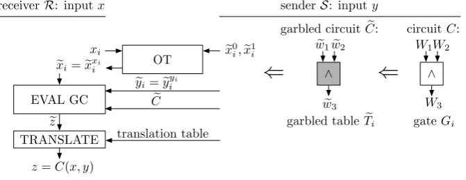
Yao’s Garbled Circuit (GC) approach [60] allows two parties, senderS with private input y and receiverRwith private inputx, to securely evaluate a boolean circuitCon (x, y) without revealing any information other than the resultz=C(x, y) of the evaluation. In particular, no intermediate values are revealed. We summarize the idea of Yao’s GC protocol next (see Fig. 1 for an overview). The circuitconstructorScreates agarbled circuitCe from the circuitC: for each wireWi ofC,
he randomly chooses two garblings we0
i,we1i, where we j
i is thegarbled valueof Wi’s value j. (Note: e
wij does not reveal j.) Further, for each gate Gi, S creates a garbled table Tei with the following
property: given a set of garbled values ofGi’s inputs,Tei allows to recover the garbled value of the
correspondingGi’s output, but nothing else.S sends these garbled tables, calledgarbled circuitCe,
toevaluator(receiverR).
Additionally,R(obliviously) obtains thegarbled inputsweicorresponding to the inputs of both
parties: the garbled inputsyecorresponding to the inputs y of S are sent directly: yei =yeiyi. For
each ofR’s inputs xi, both parties run a 1-out-of-2 Oblivious Transfer (OT) protocol (e.g., [34]),
whereSinputsex0i,ex1i andRinputsxi. The OT protocol ensures thatRreceives only the garbled
value corresponding to his input bit, i.e.,xei=exxii, whileS learns nothing aboutxi.
Now, Revaluates the garbled circuit Ce on the garbled inputs to obtain thegarbled output ez
by evaluatingCe gate by gate, using the garbled tablesTei. Finally,Rdetermines the plain valuez
corresponding to the obtained garbled output value using an output translation table sent byS. Correctness of GC follows from the way garbled tablesTeiare constructed. Yao’s garbled circuit
protocol is provably secure ([29]) when both parties are semi-honest (i.e., follow the protocol but may try to infer information about the other party’s inputs from the messages seen). We stress that each GC can be evaluated only once, i.e., a new GCCe must be used for each invocation.
Improved Garbled Circuits.We use the improved GC construction of [40], summarized next. Each garbled valuewei=hki, πiiconsists of at-bit keykiand a permutation bitπi, wheretdenotes
the symmetric security parameter. XOR gates are evaluated “for free”, i.e., no garbled table and negligible computation, by computing the bitwise XOR of their garbled values [26]. For each non-XOR gate withdinputs the garbled tableTei consists of 2d−1 entries of sizet+ 1 bits each; the
evaluation of a garbled non-XOR gate requires one invocation of SHA-256 [40]. At the high level, the keyski of the non-XOR gate’s garbled inputs are used to obtain the corresponding garbled
output value by decrypting the garbled table entry which is indexed by the input permutation bits
πi. We present the detailed description of the construction in Appendix§A.
2.2 Non-Interactive Garbled Circuits and One-Time Programs
receiverR: inputx
circuitC: senderS: inputy
� C OT
� z EVAL GC
� xi=�xxii
xi
z=C(x, y) TRANSLATE
� x0
i,�x1i
� yi=y�iyi
translation table
garbled circuitC�:
⇐
gateGi
W1W2
W3
∧
garbled tableT�i
� w1w�2
� w3
∧
⇐
Fig. 1.Overview of Yao’s Garbled Circuit Protocol (AND gate as example circuit)
the round complexity and (non-)interactivity features of the GC protocol are exactly those as the underlying OT.
Traditionally, for computational and storage efficiency, and because considered client-server applications permitted it, OT was considered in the interactive setting. In [15] the authors suggested to extend the Trusted Platform Module (TPM) [55] for implementing non-interactive OT, resulting in a non-interactive version of Yao’s protocol. Subsequently, One-Time Programs (OTP) were introduced in [13]. This approach considers malicious receivers and can be viewed simply as Yao’s Garbled Circuit (GC), where the oblivious transfer (OT) function calls are implemented with One-Time Memory (OTM) tokens. An OTM tokenTi is a simple tamper-proof hardware, which allows
a single query of one of the two stored garbled valuesxe0
i,xe1i ([13] suggests using a tamper-proof
one-time-settable bit bi which is set as soon as the OTM is queried).6 Further, OTM-based GC
execution can be non-interactive, in the sense that the sender can send the GC and corresponding OTMs to the receiver, who will be able to execute one instance of SFE on any input of his choice.7 Finally, GC (and hence also OTP) is inherently a one-time execution object (generalizable to
k-time execution by repetition).
A subtle issue in this context, noted and addressed in [13], is the following. Previous GC-based solutions were either in the semi-honest model, or used interaction during protocol execution, which precluded the receiver R from choosing his input adaptively, based on given (and even partially evaluated) garbled circuit. This possibility of adaptively chosen inputs results in possible real attacks by a malicious receiver R in the non-interactive setting.8 The solution of [13] is to mask (each) output bit zj of the function with a random bit mj, equal to XOR of (additional)
random bits mi,j contributed by each of the input OTMs Ti, i.e., mj = m1,j ⊕m2,j ⊕. . . and
z0
j =zj⊕mj. The real-world adversary does not learn the output of the function before he had
queried all OTMs with his inputs, which precludes him from adaptively selecting the input.9In §3 we present an efficiency improvement, and a generic architecture for leakage-resilient and tamper-proof computation derived from OTP.
6 Indeed, this is one of the simplest functionalities possible, and one that is hopefully easier to protect
against leakage and tampering (we refer the reader to [13] for extended discussion on such protection). 7
As also noted in [14], the function can be fully hidden by evaluating a universal function instead. In practice, one would evaluate a garbledUniversal Circuitthat is programmed to compute the intended function. For ak-gate function, the universal circuit constructions of [56, 27, 43] result in an overhead of O(klogk),O(klog2k) andO(k2) gates respectively with decreasing constant factors.
8
From the mathematical perspective, the standard proof of security of GC now does not go through, since the simulatorSimwould have to output toRthe simulated garbled circuit (i.e., its garbled tables and output wire decoding) before knowing the inputs of the malicious receiver.
9
3
Extending and Using One-Time Programs
In§3.1 we present an extension of the OTP construction of [13], which results in improved per-formance for multiple outputs. Additionally we make several observations about uses, security guarantees and applicability of OTP, and present a generic architecture for using OTPs for leakage-resilient computation in§3.2.
3.1 Extending One-Time Programs
As mentioned in the previous section, the solution in [13] seems to require each OTM token to additionally store a string of the size of the output. We propose a practical performance improve-ment to the technique proposed in [13], which is beneficial for OTP evaluation of functions with many output bits. In our solution each OTM token (additionally) stores a random string ri of
length of the security parametert. Consequently, our construction results in smaller OTMs when the function to be evaluated has more outputs than the size of the security parametert. As a trade off, our security proof utilizes Random Oracles (RO), as we do not immediately see how to avoid their use and have OTM size independent of the number of outputs. We discuss RO, its uses and security guarantees in Appendix§C.
Our main idea is to insert a “hold off” gate into each output wire Wj which can only be
evaluated onceallinput OTMs had been queried, thus preventing malicious Rfrom choosing his input adaptively. It can be implemented by requiring a call to a hash function H (modeled as a Random Oracle) with inputs which include data from all OTMs. To implement this, we secret-share a random value r ∈R {0,1}t over all OTMs for the inputs. That is, OTM Ti additionally
stores a share ri (released to Rwith exi upon the query), where r=L i
ri. ReceiverRis able to
recoverrif and only if he queried all OTMs.
Fig. 2(b) depicts this contruction: Our version of OTMTi, in addition to the two OT secrets e
x0
i,xe1i and the tamper-proof bitbi, contains a random shareri∈R{0,1}twhich is released together
withxexi
i onceTiis queried with input bitxi. The GC is constructed as usual (e.g., as described in
§2.1), with the following exception. On each output wireWjwith garbled outputsez0j,ez1j, we append
a one-input, one-output OT-commit gateGj, with no garbled table. We set the output wire secrets
ofGj tobzj0=H(ez0j||r),bzj1=H(ez1j||r). To enableRto compute the wire output non-interactively,
GC also specifies thatzbb
j corresponds tob.
We note that a full formal construction is readily obtained from the above description. Also note that a maliciousRis unable to complete the evaluation of any wire of GC until all the OTMs have been queried, and his input has been specified in full. Further, he is not able to lie about the result of the computation, since he can only compute one of the two valuesez0
j,ez1j. Demonstration
of knowledge ofezi
j serves as a proof for the corresponding output value.
Theorem 1. The above protocol is secure against a semi-honest senderS, who generates the OTM tokens and the garbled circuit, and malicious receiverR, in the Random Oracle model.
Proof. The proof of Theorem 1 is given in Appendix §B. ut
3.2 Using One-Time Programs for Leakage Protection
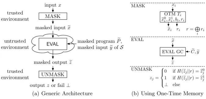
Most of today’s countermeasures to side-channel attacks are specific toknownattacks. Protecting hardware implementations (e.g., of AES) usually proceeds as follows (e.g., see [2]). First, the inputs are hidden, typically by applying a random mask (this requires trusted operation, and often the corresponding assumption is introduced). Afterwards, the computation is performed on the masked data. To allow this, the functionality needs to be adapted (e.g., using amended AES S-boxes). Finally, the mask is taken off to reveal the output of the computation.
We use a similar approach with similar assumptions (cf. Fig. 2(a)) to provably protectarbitrary functionalities againstallattacks, both known and unknown:
2. The computation on the masked data is performed in an untrusted environment where the adversary is able to arbitrarily interfere (passively and actively) with the computation. To compute on the masked data, the evaluation algorithm EVAL needs a specially masked version of the programPe. Additional masked inputseyofS that are independent ofR’s inputs can be provided as well. The result of EVAL is the masked outputez.
3. Finally, ez is unmasked into the plain output z. The procedure UNMASK allows to verify that ez was computed correctly, i.e., no tampering happened in the EVAL phase in which case UNMASK outputs the failure symbol ⊥. For correctness of this verification, UNMASK is executed in a trusted environment where the adversary can observe but not modify the computation.
masked input�x
masked output�z
outputzor fail⊥
UNMASK
EVAL
inputx
MASK
untrusted environment
trusted environment
trusted environment
masked programP�, masked inputy�ofS
(a) Generic Architecture
xi
� xi OTMTi � x0
i,�x1i, bi, ri
ri
� x
EVAL GC C,� �y
� z MASK
EVAL
UNMASK
r=� i
ri
zj=
0 ifH(zj�||r) =z�0
j 1 ifH(zj�||r) =z�1
j
⊥ else
(b) Using One-Time Memory
Fig. 2.Evaluating a Functionality Without Leakage
More specifically, the masked programPeis a garbled circuitCe, masked valuesx,e ey,zeare garbled values and the algorithms MASK, EVAL and UNMASK can be implemented as described next.
MASK: Masking the input dataxof receiver Ris performed by mapping each bit xi to its
corresponding garbled valuexei, i.e., to one of two garblingsxe0i,xe1i. This can be provided externally
(e.g., by interaction with a party on the network). We concentrate on on-boardnon-interactive masking which requires certain hardware assumptions (see below). The following can be directly used as a (non-interactive) MASK procedure:
– OTMs [13]: For small functionalities, we favor the very cheap One-Time Memory (OTM), as this seems to carry the weakest assumptions (cf. §2.2). However, as OTMs can be used only once, a fresh OTM must be provided for each input bit of the evaluated functionality. For practical applications, OTMs (together with their garbled circuits) could be implemented for example on tamper-proof USB tokens for easy distribution.
– TPM [15]: Trusted Platform Modules (TPM) are low-cost tamper-proof cryptographic chips embedded in many of today’s PCs [55]. TPM masking based on the non-interactive Oblivious Transfer (OT) protocol of [15] requires the (slightly extended) TPM to perform asymmetric cryptographic operations in form of a count-limited private key whose number of usages is restricted by the TPM chip. An interactive protocol allows re-initialization for future non-interactive OTs instead of shipping new hardware.
– Smartcard: In our preferred solution for larger functionalities, masking could be performed by a tamper-proof smartcard. The smartcard would keep a secure monotonic counter to ensure a single query per input bit. Another advantage of this approach is that the same smartcard can be used to generate GC as well, thus eliminating GC transfer over the network as done in [19]. Further, the smartcard can be naturally used for multiple OTP evaluations.
EVAL: The main technical contribution of this paper, the implementation of EVAL (of the masked programPe on masked inputsxeand ey) in embedded systems is presented in detail in§4. Here we note thatPeandey(masked input ofS) can be generated offline by the semi-honest sender S and provided to EVAL by convenient means (e.g., via a data network or a storage medium). This is the scenario advocated in [13]; one of its advantages is that generation ofPe does not leak to EVAL. Alternatively,Pe and ey could be generated “on-the-fly” using a cheap simple constant-memory stateless and tamper-proof token as shown in [19]. We reiterate that the masked program
e
P can be evaluated exactly once.
UNMASK: Finally, the masked output ze is checked for correctness and non-interactively decoded byR into the plain output z as follows (cf. §3.1 and Fig. 2(b)). For each output wire, the masked programPe specifies the correspondencebzj →zj in form of the two valid hash values b
z0
j and bz1j. Even if EVAL is executed in a completely untrusted environment (e.g., processed on
untrusted HW), its correct execution can be verified efficiently: whenH(zej||r) is neitherbz0j norzbj1
the garbled outputzej is invalid and UNMASK outputs the failure symbol⊥. The reason for this
verifiability property of GC is that a valid garbled output ezj can only be obtained by correctly
evaluating the GC but cannot be guessed.
How far can we go with Homomorphic Encryption.At the first glance, the recently proposed Fully Homomorphic Encryption (FHE) [11, 7, 47] may seem as an attractive alternative solution for leakage-free computation. Indeed, FHE allows to compute arbitrary functions on encrypted data without the need for helper data in form of a masked program. The MASK algorithm would homomorphically encrypt the inputxand the UNMASK algorithm could decrypt the result. Using verifiable computation [10], fully homomorphic encryption can also be extended to allow verification that the computation was performed correctly.
However, we argue that FHE is in fact not appropriate in our setting: Our first comment, which concerns any application of FHE, is that, in its state today, FHE is extremely computationally intensive. Although significant effort is underway in theoretical community to improve its perfor-mance, it seems unlikely that FHE would reach the efficiency of current public-key encryption schemes. Intuitively, this is because FHE must provide the same strong security guarantees, while, at the same time, possessing extra algebraic structure to allow for homomorphic operations. The extra structure weakens security, and countermeasures (costing performance) are necessary. Fur-ther, even assuming performance similar to that of RSA, this solution would be hundreds of times slower than GC-based solution, as symmetric primitives used in GC are orders of magnitude faster. Finally, from the leakage-resilience perspective, the UNMASK algorithm will be problematic, as it would need to perform complicated decryptions based on secret key. We would need to ensure nothing is leaked in these modules, which would bring us either to using much stronger assumptions or to a chicken-and-egg problem.
4
Efficient Evaluation of Garbled Circuits in Hardware
In this section we describe how GCs (and hence also OTPs) can be efficiently evaluated on embed-ded systems and memory-constrained devices. We first describe the HW architecture in§4.1. Then we present important compile-time optimizations and show their effectiveness in§4.2. Finally, we discuss technical details of our prototype implementation and timings in§4.3.
We stress that our designs and optimizations are generic. However, for concreteness and for meaningful comparison (e.g., with prior SW SFE of AES [40]), we take SFE of the AES function as our example for timings and other measurements. AES was chosen by [40] as a useful and representative function, with applications such as Oblivious Pseudo-Random Functions (OPRF), side-channel protection, blind MACs and encryption, and computation on encrypted data.
4.1 Architecture for Evaluating Garbled Circuits in Hardware
We describe our architecture for efficient evaluation of GC on memory-constrained devices, i.e., having a small amount of slow memory only.
To minimize overhead, we choose key length t= 127; with a permutation bit, garbled values are thus 128 bits long (cf.§2.1). In the following we assume that memory cells and registers store 128 bit garbled values. This can be mapped to standard hardware architectures by using multiple elements in parallel.
Fig. 3 shows a conceptual level overview of our architecture described next. At the high-level, EVAL, the process of evaluating GC, on our architecture consists of the following steps (cf. §3.2). First, the garbled input valuesx,e eyare stored in memory using the I/O interface. Then, GC gates are evaluated, using registers A, B, and C to cache the garbled inputs and outputs of a single garbled gate. Finally, garbled output valueezis output over the I/O interface.
Eval Gate
Garbled Tables
OUT I/O
(1
or
2)
of
3
XOR AC EVAL A/B/C EVAL AB/AC/BC
M
em
or
y
(m
em
)
STORE C LOAD A
LOAD B STORE A
STORE B XOR A
XOR B
XOR C Reg C
Reg B Reg A
XOR AB
XOR BC
� x,�y
�
z SHA-256
Fig. 3.Architecture for GC Evaluation (EVAL) on Memory-Constrained Devices
As memory access is expensive (cf.§4.3) we optimize code to re-use values already in registers. Our instructions are one-address, i.e., each instruction consists of an operator and up to one memory address. Each of our instructions has length 32 bits: 5 bits to encode one of 18 instructions (described next) and 27 bits to encode an address in memory.
LOAD/STORE: Registers can be loaded from memory using instructions LOAD A and
LOAD B. Register C cannot be loaded as it will hold the output of evaluated non-XOR gates (see below). Values in registers can be stored back into memory using STORE A, STORE B, and STORE C respectively.
XOR: We evaluate XOR gates [26] as follows. XOR Aaddr computesA ←A⊕mem[addr]. Similarly, the other one-operand XOR operations (XOR1) XOR B and XOR C xor the value from memory with the value in the respective register. To compute XOR gates where both inputs are already in registers (XOR2), the instruction XOR AB computesA←A⊕B. Similarly, XOR AC computesA←A⊕C and XOR BC computesB ←B⊕C.
EVAL:Non-XOR gates [40] are evaluated with the Eval Gate block that contains a hardware accelerator for SHA-256 (cf. §2.1 for details). The garbled inputs are in one (EVAL1) or two registers (EVAL2), and the result is stored in register C. The respective instructions for 1-input gates are EVAL A, EVAL B, EVAL C and for 2-input gates EVAL AB, EVAL AC, EVAL BC. The required garbled table entry is read from memory.
I/O:The garbled inputs are always stored at the first|x|+|y|memory addresses. The garbled outputs are obtained from memory with OUT instructions.
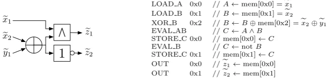
Example 1. Fig. 4 shows an example circuit and a possible sequence of instructions to evaluate it on our architecture. First, register A is loaded with ex1 from memory address 0x0, thenxe2⊕ye1 is computed in register B and the AND gate is evaluated to obtain outputze1 which is stored at address 0x0 and overwritesxe1, which is no longer needed. Then, the NOT gate is computed using register B as input and stored at address 0x1. The two outputsez1,ez2are at addresses 0x0 and 0x1.
4.2 Compile-time Optimizations for Memory-Constrained Devices
� �
x1
� x2
�
y1
1
� z1
� z2
LOAD A 0x0 //A←mem[0x0] =ex1
LOAD B 0x1 //B←mem[0x1] =ex2
XOR B 0x2 //B←B⊕mem[0x2] =ex2⊕ey1
EVAL AB //C←A∧B
STORE C 0x0 // mem[0x0]←C
EVAL B //C←notB
STORE C 0x1 // mem[0x1]←C
OUT 0x0 //ez1←mem[0x0]
OUT 0x1 //ez2←mem[0x1]
Fig. 4.Example Circuit (left) and Instruction Sequence to Evaluate its GC on our Architecture of Fig. 3 (right).
the number of non-XOR gates), the size of the program (number of instructions), the number of memory accesses and memory size for storing intermediate garbled values. For concreteness, we use AES as representative functionality for the optimizations and performance measurements, but our techniques are generic.
Optimization a:Base [40])Our baseline is the AES circuit/code of [40], already optimized for a small number of non-XOR gates. Their circuit consists of 11,286 two-input non-XOR gates; thus, its GC has size 11,286·3·128 bit≈529 kByte. Without considering any caching strategies, this results in 113,054 instructions, hence the program size is 113,054·32 bit ≈442 kByte, and the total amount of memory needed for EVAL is 34,136·128 bit≈533 kByte.
We start with further reduction of the size of the garbled circuit.
Optimization b:NoXNOR)We reduce the GC size by replacing XNOR gates with XOR gates, and propagating the inverted output into the successor gates. Output XNOR gates are replaced with XOR and a 1-input inverter gate. The cost of this optimization is linear in the size of the circuit [38]. Overall, this optimization results in the elimination of 4,086 XNOR gates and reduces the size of AES GC to (7,200·3 + 40)·128 bit≈338 kByte (improvement of 36%).
Remaining optimizations use b:NoXNOR; d:MaxFanout, e:Rand use c:Cache.
Optimization c:Cache)We re-use values already in registers to reduce the number of LOADs. Values in registers are saved to memory only if needed later.
Optimization d:MaxFanout)We select a specific topologic order (traversing the circuit depth-first and following children in decreasing order of their fan-out).
Optimization e:Rand)We randomly consider several orders of evaluation, and select the most efficient one for EVAL. (This is a one-time compilation expense per function.) For present work, we considered several random topologic orders of the circuit, constructed by the traversal where the next gate is selected at random from the set of unprocessed gates with maximal fan-out. A more rigorous approach to this randomized technique can result in more substantial improvement, and is a good direction for future work.
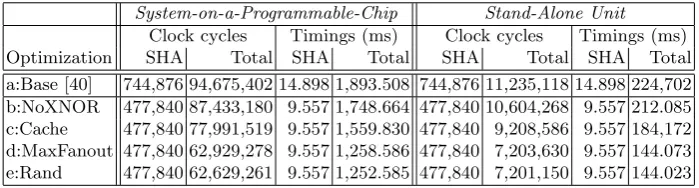
Result.Using our optimizations we were able to substantially decrease the memory footprint of EVAL. As shown in Table 1 the smallest program was obtained with the non-deterministic opti-mization e:Rand which is only slightly better than our best deterministic optiopti-mization d:MaxFanout and improves over a:Base [40]as follows. The size of the AES programP is only 73,583·32 bit≈ 287 kByte (improvement of 34.9%). The amount of intermediate memory is 17,315·128 bit ≈ 271 kByte (improvement of 49.3%) and the number of memory accesses (read and write) is re-duced by≈35%.
Table 1.Optimized AES Circuits (Sizes in kB)
4.3 Implementation
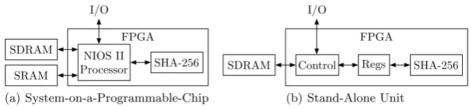
We have designed two prototype implementations of the architecture of§4.1 – one for a System-on-a-Programmable-Chip with a hardware accelerator for SHA (reflecting smartcard and future smartphone architectures) and another for a stand-alone unit (reflecting a custom-made GC ac-celerator in hardware). Both prototype implementations are evaluated on an Altera/Terasic DE1 FPGA board comprising an Altera Cyclone II EP2C20F484C7 FPGA and 512kB SRAM and 8MB SDRAM (and several other peripherals that are not relevant for this work) and are functionally equivalent: they take the same inputs (programP, garbled circuitCe, and garbled inputsex,ye) and return the same garbled outputsez; the only differences are the methods used in the implementa-tion. The interfaces (I/Os in Fig. 5) allow the host to write to and read from the SDRAM. In the beginning, the host writes the inputs to the SDRAM and, in the end, the outputs are written into specific addresses from which the host retrieves them.
SDRAM
SRAM
NIOS II Processor
FPGA I/O
SHA-256
(a) System-on-a-Programmable-Chip
SDRAM Control SHA-256
FPGA I/O
Regs
(b) Stand-Alone Unit
Fig. 5.Architectures for Hardware-Assisted GC Evaluation
System-on-a-Programmable-Chip (SOPC). Our first implementation is a system-on-a-programmable-chip (SOPC) consisting of a processor with access to a hardware accelerator for SHA-256, which speeds up the most computational burden of the GC evaluation. This is a rep-resentative architecture for next generation smartphones or smartcards such as the STMicroelec-tronics ST33F1M smartcard which includes a 32-bit RISC processor, cryptographic peripherals, and memory comparable to our prototype system [51].
The architecture of our implementation is shown in Fig. 5(a). It consists of a NIOS II/e 32-bit softcore RISC processor (the smallest variation of NIOS II), a custom-made SHA-256 unit, the SRAM, and the SDRAM. The entire process is run in the NIOS II processor which uses the SHA-256 unit for accelerating gate evaluations. The SHA-256 unit is connected to the Avalon bus of the NIOS II as a peripheral component and it computes the hash for a 512-bit message in 66 clock cycles (excluding interfacing delays). The NIOS II program, etc., are stored in the SRAM and the SDRAM is devoted solely for the data required to execute an OTP, i.e., the program for our architecture, the garbled circuit, the garbled inputs, the intermediate garbled values, etc.
Stand-Alone Unit.Our second implementation is a stand-alone unit consisting of a custom-made control state machine, registers (A, B, C), a custom-custom-made SHA-256 unit, and SDRAM. This architecture could be used to design an Application Specific IC (ASIC) as high-speed hardware accelerator for GC evaluation. The architecture is depicted in Fig. 5(b).
When the host has written the inputs to the SDRAM, the stand-alone unit executes the pro-gram. The state machine parses the program and reads/writes data from/to SDRAM to/from the registers or evaluates the non-XOR gates using the SHA-256 unit according to the instructions (see§4.1 for details).
Prototyping Environment. The implementations were synthesized with Altera Quartus II, version 9.1 (2009). The custom-made units were written with VHDL and verified with simulations in ModelSim Altera-edition, version 6.5b (2009). The NIOS II processor was programmed with C using NIOS II IDE, version 9.1 (2009). All parts of both implementations run with a 50 MHz clock. The interfacing with the host was implemented with NIOS II also for the stand-alone unit. In both implementations, data was transferred to the FPGA by using theHost File System (HFS) of NIOS II; we point out that HFS is feasible for prototyping phase only, and the interface should be replaced with a more appropriate one (e.g., PCI-Express or Gigabit Ethernet) in a real application.
(LUT) and a flip-flop (FF), and 52 4096-bit embedded memory blocks (M4K). The values of the stand-alone unit exclude NIOS II used for the HFS in the prototype. SHA-256 is the largest and most significant block in both prototypes. The SOPC additionally contains NIOS II, on-chip memory, and S(D)RAM controller, and the stand-alone unit contains additional control logic, registers, and SDRAM controller (cf. Fig. 5).
Table 2 also shows the area for a straightforward iterative implementation of AES-128 on the same FPGA to ease cost evaluation of our methodology; however, this implementation does not include any countermeasures against side-channel attacks. Compared to an unprotected implemen-tation, countermeasures against power analysis have area overheads ranging from factor of 1.5 to 5 [52] as discussed in§1.2; therefore, the area overheads of OTP evaluation are comparable with other side-channel countermeasures.
Table 2.Areas of the Prototypes for GC Evaluation on an Altera Cyclone II FPGA
Design LC FF M4K
SOPC 7501 4364 22
NIOS II 1104 493 4 SHA-256 2918 2300 8
Stand-Alone Unit 6252 3274 8
SHA-256 3161 2300 8
AES (unprotected) 2418 431 0
Table 3. Timings for Instructions on Prototypes (clock cycles, average)
Instruction SOPC Stand-Alone Unit
LOAD 291.43 87.63
XOR1 395.30 87.65
XOR2 252.00 1.00
STORE 242.00 27.15
EVAL1 1,282.30 109.95 EVAL2 1,491.68 135.05
OUT 581.48 135.09
Timings.Instructions.The timings of instructions are summarized in Table 3. They show the average number of clock cycles required to execute an instruction excluding the latency of fetching the instruction. Gate evaluations are expensive in the SOPC implementation, although the SHA-256 computations are fast, because they involve a lot of data movement (to/from the SHA-SHA-256 unit and from the SDRAM) which is expensive. The dominating role of memory reads and writes is clear in the timings of the stand-alone implementation: the only instructions that do not require memory operations (XOR2) require only a single clock cycle and EVAL1 is faster than EVAL2 because it accesses the memory on average every other time (no access if the permutation bit is zero) compared to three times out of four (no access if both permutation bits are zeros).
AES. The timings to evaluate the optimized GCs for the AES functionality of §4.2 on our prototype implementations are given in Table 4. These timings are for GC evaluation only; i.e, they neglect the time for transferring data to/from the system because interface timings are highly technology dependent (HFS is extremely slow, but convenient for prototyping). The SHA-256 computations take an equal amount of time for both implementations as the SHA-256 unit is the same. The (major) difference in timings is caused by data movement, XORs, interface to the SHA-256 unit, etc. The runtimes for both implementations are dominated by writing and reading the SDRAM; e.g., 84.3% for the stand-alone unit and our smallest AES circuit (optimization e:Rand). Hence, accelerating memory access, e.g., with burst reads and writes, is the key for further speedups.
Table 4.Timings for the FPGA-based Prototypes for GC Evaluation
System-on-a-Programmable-Chip Stand-Alone Unit
Performance Comparison. A software implementation that evaluates the GC/OTP of the un-optimized AES functionality a:Base [40] required 2 seconds on an Intel Core 2 Duo 3.0 GHz with 4GB of RAM [40]. Our optimized circuit e:Rand evaluated on the stand-alone unit requires only 144 ms for the same operation and, therefore, provides a speedup by a factor of 10.4–17.4 (taking the lack of precision into account).
On the other hand, the unprotected AES implementation listed in Table 2 encrypts a message block in 10 clock cycles and runs on a maximum clock frequency of 66 MHz resulting in a timing of 0.1515µs; hence, the GC/OTP evaluation suffers from a timing overhead factor of≈950,000. For comparison, the timing overhead of one specific implementation with countermeasures against differential power analysis was factor of 3.88 [53].
5
Conclusion
The power of side-channels attacks on cryptographic implementations have motivated both theo-reticians and practitioners to seek more general defense models and solutions. The recent strand of research on leakage-resilient cryptography is still in its early stage, and most proposals are not yet implemented and evaluated in practice. The recent observation of one-time programs (OTPs) uses established Garbled Circuit (GC) techniques, and relies on hardware with relatively weak tamper-proof assumptions, to realize provably leakage-resilient evaluation of arbitrary functions in an untrusted environment.
In this work, we studied the performance of GC/OTP evaluation in hardware. For this, we implemented two hardware prototypes for GC/OTP evaluation based on FPGA: one for a system-on-a-programmable-chip with access to a hardware accelerator for SHA-256 (representative for smartcards and future smartphones), and a stand-alone hardware implementation (reflecting a custom-made GC accelerator in hardware). We chose AES as the representative complex function, and we believe our measurements will serve as a reference point for estimating runtimes of a variety of useful functions.
Our measurements show an order of magnitude performance improvement over the previous software implementation of AES GC evaluation reported in [40]. We thus believe that GC/OTP is a viable option for hardware implementation, especially for secure computation scenarios, where hardware acceleration is desired. The use of GC/OTP for leakage resilience carries high cost, and should be reserved for truly security-critical applications. Finally, OTP can be inherently evaluated only once, i.e., each additional evaluation requires fresh OTM hardware modules and data transfer for the GC (338 kByte for AES), which prevents certain deployment scenarios.
Acknowledgements. We thank anonymous reviewers of CHES’10 for their helpful comments and co-authors of [40] for the initial AES circuit.
References
1. D. Agrawal, B. Archambeault, J. R. Rao, and P. Rohatgi. The EM side-channel(s). InCryptographic Hardware and Embedded Systems (CHES’02), volume 2523 ofLNCS, pages 29–45. Springer, 2002. 2. M.-L. Akkar and C. Giraud. An implementation of DES and AES, secure against some attacks. In
Cryptographic Hardware and Embedded Systems (CHES’01), volume 2162 of LNCS, pages 309–318. Springer, 2001.
3. C. Archambeau, E. Peeters, F.-X. Standaert, and J.-J. Quisquater. Template attacks in principal subspaces. In Cryptographic Hardware and Embedded Systems (CHES’06), volume 4249 of LNCS, pages 1–14. Springer, 2006.
4. C. Cachin, J. Camenisch, J. Kilian, and J. M¨uller. One-round secure computation and secure au-tonomous mobile agents. In International Colloquium on Automata, Languages and Programming (ICALP’00), volume 1853 ofLNCS, pages 512–523. Springer, 2000.
5. R. Canetti, O. Goldreich, and S. Halevi. The random oracle methodology, revisited.J. ACM, 51(4):557– 594, 2004.
7. M. v. Dijk, C. Gentry, S. Halevi, and V. Vaikuntanathan. Fully homomorphic encryption over the integers. Cryptology ePrint Archive, Report 2009/616, 2009.http://eprint.iacr.org. To appear at EUROCRYPT 2010.
8. W. Fischer and B. M. Gammel. Masking at gate level in the presence of glitches. In Cryptographic Hardware and Embedded Systems (CHES’05), volume 3659 ofLNCS, pages 187–200. Springer, 2005. 9. K. Gandolfi, C. Mourtel, and F. Olivier. Electromagnetic analysis: Concrete results. InCryptographic
Hardware and Embedded Systems (CHES’01), volume 2162 ofLNCS, pages 251–261. Springer, 2001. 10. R. Gennaro, C. Gentry, and B. Parno. Non-interactive verifiable computing: Outsourcing computation
to untrusted workers. Cryptology ePrint Archive, Report 2009/547, 2009. http://eprint.iacr.org. 11. C. Gentry. Fully homomorphic encryption using ideal lattices. In ACM Symposium on Theory of
Computing (STOC’09), pages 169–178. ACM, 2009.
12. B. Gierlichs, L. Batina, B. Preneel, and I. Verbauwhede. Revisiting higher-order DPA attacks: Mul-tivariate mutual information analysis. InCryptographers’ Track at RSA Conference (CT-RSA ’10), volume 5985 ofLNCS, pages 221–234. Springer, 2010.
13. S. Goldwasser, Y. T. Kalai, and G. N. Rothblum. One-time programs. InAdvances in Cryptology – CRYPTO 2008, volume 5157 ofLNCS, pages 39–56. Springer, 2008.
14. V. Goyal, Y. Ishai, A. Sahai, R. Venkatesan, and A. Wadia. Founding cryptography on tamper-proof hardware tokens. InTheory of Cryptography (TCC’10), volume 5978 ofLNCS, pages 308–326. Springer, 2010.
15. V. Gunupudi and S. Tate. Generalized non-interactive oblivious transfer using count-limited objects with applications to secure mobile agents. In Financial Cryptography and Data Security (FC’08), volume 5143 ofLNCS, pages 98–112. Springer, 2008.
16. J. A. Halderman, S. D. Schoen, N. Heninger, W. Clarkson, W. Paul, J. A. Calandrino, A. J. Feldman, J. Appelbaum, and E. W. Felten. Lest we remember: Cold boot attacks on encryption keys. InUSENIX Security Symposium (Security’08), pages 45–60. USENIX Association, 2008.
17. D. Hwang, K. Tiri, A. Hodjat, B. Lai, S. Yang, P. Schaumont, and I. Verbauwhede. AES-based security coprocessor IC in 0.18-µm CMOS with resistance to differential power analysis side-channel attacks.
IEEE Journal of Solid-State Circuits, 41(4):781–791, 2006.
18. Y. Ishai, A. Sahai, and D. Wagner. Private circuits: Securing hardware against probing attacks. In
Advances in Cryptology – CRYPTO 2003, volume 2729 ofLNCS, pages 463–481. Springer, 2003. 19. K. J¨arvinen, V. Kolesnikov, A.-R. Sadeghi, and T. Schneider. Embedded SFE: Offloading server and
network using hardware tokens. InFinancial Cryptography and Data Security (FC’10), volume 6052 ofLNCS, pages 207–221. Springer, 2010.
20. K. J¨arvinen, V. Kolesnikov, A.-R. Sadeghi, and T. Schneider. Garbled circuits for leakage-resilience: Hardware implementation and evaluation of one-time programs. InCryptographic Hardware and Em-bedded Systems (CHES’10), volume 6225 ofLNCS, pages 383–397. Springer, 2010.
21. J. Kelsey, B. Schneier, D. Wagner, and C. Hall. Side channel cryptanalysis of product ciphers. In
European Sumposium on Research in Computer Security (ESORICS ’98), volume 1485 ofLNCS, pages 97–110. Springer, 1998.
22. P. Kocher, J. Jaffe, and B. Jun. Differential power analysis. InAdvances in Cryptology – CRYPTO 1999, volume 1666 ofLNCS, pages 388–397. Springer, 1999.
23. V. Kolesnikov. Gate evaluation secret sharing and secure one-round two-party computation. In ASI-ACRYPT’05, volume 3788 ofLNCS, pages 136–155. Springer, 2005.
24. V. Kolesnikov. Truly efficient string oblivious transfer using resettable tamper-proof tokens. InTheory of Cryptography (TCC’10), volume 5978 ofLNCS, pages 327–342. Springer, 2010.
25. V. Kolesnikov, A.-R. Sadeghi, and T. Schneider. Improved garbled circuit building blocks and appli-cations to auctions and computing minima. InCryptology and Network Security (CANS’09), volume 5888 ofLNCS, pages 1–20. Springer, 2009.
26. V. Kolesnikov and T. Schneider. Improved garbled circuit: Free XOR gates and applications. In
International Colloquium on Automata, Languages and Programming (ICALP’08), volume 5126 of
LNCS, pages 486–498. Springer, 2008.
27. V. Kolesnikov and T. Schneider. A practical universal circuit construction and secure evaluation of private functions. InFinancial Cryptography and Data Security (FC’08), volume 5143 ofLNCS, pages 83–97. Springer, 2008.
28. K. Lemke. Embedded security: Physical protection against tampering attacks. In C. Paar K. Lemke and M. Wolf, editors,Embedded Security in Cars, chapter 2, pages 207–217. Springer, 2006.
29. Y. Lindell and B. Pinkas. A proof of Yao’s protocol for secure two-party computation. Journal of Cryptology, 22(2):161–188, 2009. Cryptology ePrint Archive, Report 2004/175,http://eprint.iacr. org.
30. Y. Lindell, B. Pinkas, and N. Smart. Implementing two-party computation efficiently with security against malicious adversaries. InSecurity and Cryptography for Networks (SCN’08), volume 5229 of
31. D. Malkhi, N. Nisan, B. Pinkas, and Y. Sella. Fairplay — a secure two-party computation system. In
USENIX Security Symposium (Security’04). USENIX Association, 2004.
32. S. Mangard, E. Oswald, and T. Popp.Power Analysis Attacks: Revealing the Secrets of Smart Cards. Springer, 2007.
33. T. S. Messerges. Using second-order power analysis to attack DPA resistant software. InCryptographic Hardware and Embedded Systems (CHES’00), volume 1965 ofLNCS, pages 238–251. Springer, 2000. 34. M. Naor and B. Pinkas. Efficient oblivious transfer protocols. InACM-SIAM Symposium On Discrete
Algorithms (SODA’01), pages 448–457. Society for Industrial and Applied Mathematics, 2001. 35. D. A. Osvik, A. Shamir, and E. Tromer. Cache attacks and countermeasures: The case of AES. In
Cryptographers’ Track at RSA Conference (CT-RSA’06), volume 3860 ofLNCS, pages 1–20. Springer, 2006.
36. E. Oswald and S. Mangard. Template attacks on masking—resistance is futile. InCryptographers’ Track at RSA Conference (CT-RSA ’07), volume 4377 ofLNCS, pages 243–256. Springer, 2007. 37. D. Page. Theoretical use of cache memory as a cryptanalytic side-channel. Technical Report
CSTR-02-003, University of Bristol, 2002.
38. A. Paus, A.-R. Sadeghi, and T. Schneider. Practical secure evaluation of semi-private functions. In
Applied Cryptography and Network Security (ACNS’09), volume 5536 ofLNCS, pages 89–106. Springer, 2009.
39. K. Pietrzak. Provable security for physical cryptography. InWestern European Workshop on Research
in Cryptology (WEWORC’09), 2009. Survey available at http://homepages.cwi.nl/~pietrzak/
publications/Pie09b.pdf.
40. B. Pinkas, T. Schneider, N. P. Smart, and S. C. Williams. Secure two-party computation is practical. InAdvances in Cryptology – ASIACRYPT 2009, volume 5912 ofLNCS, pages 250–267. Springer, 2009. 41. T. Popp and S. Mangard. Masked dual-rail pre-charge logic: DPA-resistance without routing contraints. InCryptographic Hardware and Embedded Systems (CHES’05), volume 3659 ofLNCS, pages 172–186. Springer, 2005.
42. J.-J. Quisquater and D. Samyde. Electromagnetic analysis (EMA): Measures and countermeasures for smart cards. InResearch in Smart Cards (E-smart 2001), volume 2140 of LNCS, pages 200–210. Springer, 2001.
43. A.-R. Sadeghi and T. Schneider. Generalized universal circuits for secure evaluation of private func-tions with application to data classification. InInternational Conference on Information Security and Cryptology (ICISC’08), volume 5461 of LNCS, pages 336–353. Springer, 2008.
44. M. Saeki, D. Suzuki, K. Shimizu, and A. Satoh. A design methodology for a DPA-resistant cryp-tographic LSI with RSL techniques. InCryptographic Hardware and Embedded Systems (CHES’09), volume 5747 ofLNCS, pages 189–204. Springer, 2009.
45. A. Satoh, T. Sugawara, N. Homma, and T. Aoki. High-performance concurrent error detection scheme for AES hardware. In Cryptographic Hardware and Embedded Systems (CHES’08), volume 5154 of
LNCS, pages 100–112. Springer, 2008.
46. S. P. Skorobogatov. Data remanence in flash memory devices. InCryptographic Hardware and Em-bedded Systems (CHES’05), volume 3659 ofLNCS, pages 339–353. Springer, 2005.
47. N. P. Smart and F. Vercauteren. Fully homomorphic encryption with relatively small key and cipher-text sizes. InPublic Key Cryptography (PKC’10), volume 6056 of LNCS, pages 420–443. Springer, 2010.
48. S. W. Smith. Fairy dust, secrets, and the real world. IEEE Security & Privacy, 1(1):89–93, 2003. 49. F.-X. Standaert, O. Pereira, Y. Yu, J.-J. Quisquater, M. Yung, and E. Oswald. Leakage resilient
cryptography in practice. Cryptology ePrint Archive, Report 2009/341, 2009. http://eprint.iacr. org/.
50. M. Stevens, A. Sotirov, J. Appelbaum, A. K. Lenstra, D. Molnar, D. A. Osvik, and B. d. Weger. Short chosen-prefix collisions for MD5 and the creation of a rogue CA certificate. InAdvances in Cryptology – CRYPTO 2009, volume 5677 ofLNCS, pages 55–69. Springer, 2009.
51. STMicroelectronics. Smartcard MCU with 32-bit ARM SecurCore SC300 CPU and 1.25 Mbytes high-density Flash memory. Data brief, October 2008.
http://www.st.com/stonline/products/literature/bd/15066/st33f1m.pdf.
52. K. Tiri. Side-channel attack pitfalls. InDesign Automation Conference (DAC’07), pages 15–20. ACM, 2007.
53. K. Tiri, D. Hwang, A. Hodjat, B.-C. Lai, S. Yang, P. Schaumont, and I. Verbauwhede. Prototype IC with WDDL and differential routing — DPA resistance assessment. InCryptographic Hardware and Embedded Systems (CHES ’05), volume 3659 ofLNCS, pages 354–365. Springer, 2005.
55. Trusted Computing Group (TCG). TPM main specification. Main specification, Trusted Computing Group, May 2009.http://www.trustedcomputinggroup.org.
56. L. G. Valiant. Universal circuits (preliminary report). InACM Symposium on Theory of Computing (STOC’76), pages 196–203. ACM, 1976.
57. I. Verbauwhede and P. Schaumont. Design methods for security and trust. In Design, Automation and Test in Europe (DATE’07), pages 672–677. ACM, 2007.
58. X. Wang, Y. L. Yin, and H. Yu. Finding collisions in the full SHA-1. InAdvances in Cryptology – CRYPTO 2005, volume 3621 ofLNCS, pages 17–36. Springer, 2005.
59. S. H. Weingart. Physical security devices for computer subsystems: A survey of attacks and defences. InCryptographic Hardware and Embedded Systems (CHES’00), volume 1965 ofLNCS, pages 302–317. Springer, 2000.
60. A. C. Yao. How to generate and exchange secrets. InIEEE Symposium on Foundations of Computer Science (FOCS’86), pages 162–167. IEEE, 1986.
A
Improved Garbled Circuits
Yao’s original GC construction has been improved by reducing its computation and communica-tion complexity as described next. As throughout the entire paper we denote symmetric security parameter witht.
Free XOR gates.An efficient method for creating garbled circuits which allows “free” evaluation of XOR gates was presented in [26]. More specifically, a garbled XOR gate has no garbled table (no communication) and its evaluation consists of XORing its garbled input values (negligible computation). The main observation of [26] is, that the constructorS randomly chooses a global key difference∆∈R{0,1}twhich remains unknown to evaluatorRand relates the garbled values
as we0
i = wei1⊕(∆||1). The usage of such garbled values allows forfree evaluation of XOR gates
with input wiresW1, W2and output wireW3by computingwe3=we1⊕we2 (no communication and negligible computation).
Reduced non-XOR gates. Non-XOR gates, can be evaluated as in Yao’s GC construction [60] with apoint-and-permute technique(as used in [31]): The garbled valueswei=hki, πii ∈ {0,1}t+1consist
of a symmetric keyki∈ {0,1}tand a random permutation bitπi∈ {0,1}. The entries of the garbled
table are permuted such that the permutation bitsπi of a gate’s garbled input wires can be used
as index into the garbled table to directly point to the entry to be decrypted. After decrypting this entry using the garbled input wires’t-bit keyski, evaluator obtains the garbled output value of the
gate. The encryption is done with the symmetric encryption functionEncsk1,...,kd(m), wheredis the number of inputs of the gate andsis a unique identifier used once, e.g., a monotonic gate counter.
Enccan be instantiated withm⊕H(k1||. . .||kd||s), whereHis a Random Oracle (RO) which can
be instantiated with a suitably chosen cryptographic hash function such as SHA-256 in practice. We note that the RO assumption can be avoided or weakened at small additional computation cost – see [40]. Additionally, garbled row reduction of [40] allows to remove the first entry from the garbled tables of non-XOR gates, i.e., the garbled table of ad-input non-XOR gate consists of 2d−1 table entries of sizet+ 1 bits each.
B
Proof of Theorem 1.
Proof. (sketch) Security against semi-honestS is trivial asS does not seeR’s input (we consider OTMs a separate entity fromS).
We now describe the simulatorSimwhich will produce a view indistinguishable from the view ofRin real execution.Simwill query the receiverRas a black box and answer all ofR’s queries, including calls to (simulated) ROO. Our proof is based on the idea thatSim will “program”O such that the output of the “hold off” gates will match the output given by the trusted party of the ideal game.
Without loss of generality, we assume that R queries RO only once for each distinct input. Upon initialization,Simconstructs GC, as would an honestSin the construction described above, and sends the GC toRtogether with randomly chosen commitments bz0
j,bz1j for all output wires.
Additionally,Sim generates a random keyrand a random secret sharing r=L
i
ri of it. For the
queries thei-th OTM with input bit xi, Simresponds with the corresponding garbled valuexexii,
constructed earlier as part of GC construction, and the shareri. Once R had queried the final
OTM,Simsends the input received from Rto the trusted party, and receives the output f(x, y) of the computation. NowSim “programs”O to output certain values according to the received
f(x, y). That is, on input (ezj||r) (call associated with OT-commit gate Gi and thej-th bit of the
output),O will outputbzfj(x,y)
j , i.e., the commitment for the wire leavingGj that corresponds to
the bitfj(x, y) of the output he received from the trusted party.
It is not hard to see that the above simulator generates view indistinguishable from the view of R in real execution. First, we note that the simulated GC and responses to RO and OTM queries are indistinguishable from real execution. Thus, in particular,R“behaves normally” during the simulation, and would not be able to, e.g., substitute inputs in a special way, etc. Further, “programming” ofOwill not be noticed by R, since he can query programmed values only with negligible probability prior to completing all OTM calls (since r is random and unknown to R
prior to completing all OTM calls). ut
C
On our use of Random-Oracle
We note that in our extension of one-time programs described in§3.1, we use a relatively strong assumption of programmable RO. In fact, it had been shown [5] that some (contrived) uses of RO cannot be securely instantiated withany hash function. Therefore, proofs in the RO model cannot be seen as proofs in the strictest mathematical sense. However, we believe that modeling cryptographic hash functions, such as SHA-256, as RO is well-justified in our setting.
Firstly, to date, no attacks exploiting the RO assumption are known on practical systems. This holds true even in academic context10. Further, even in well-understood and deployed real-life systems, the crypto core (which includes the employed hash functions) is almost never targeted for attacks, in favor ofmucheasier to exploit implementation flaws. In our setting, we deal with much less understood physical leakage, and make strong assumptions on the amount and content of leakage. We believe that exploiting the structure of real hash function (required to violate the RO assumption), something that eluded cryptographers for decades, is far harder and costlier than violation of other assumptions used in design of leakage-resilient systems.
In sum, we strongly believe that making the RO assumption on the employed hash function is practically justified in ours and many other settings.
10