An Efficient Coplanar Retransmission Type Chipless RFID Tag
Based on Dual-Band MCSRR
Md. Shakil Bhuiyan* and Nemai C. Karmakar
Abstract—In this paper, an efficient spectral signature based chipless RFID tag is presented, where 4N number of words can be coded using only N number of resonators. As data bit encoding element, the proposed tag utilizes a number of modified complementary split ring resonators (MCSRR). A novel resonance detuning mechanism proposed here allows the use of an MCSRR to independently encode two data bits instead of one bit. Compared with two separate rings based CSRR, the proposed MCSRR occupies 56% less area and also reduces the resonance bandwidth requirement by more than 60%. The multiresonator circuit and the UWB antennas are implemented on a thin (0.127 mm) substrate with only single sided metallization. The proposed tag has great prospect to yield an ultra-low cost chipless RFID tag that may replace barcode in the long run.
1. INTRODUCTION
As chipless radio frequency identification (RFID) technology has the potential to offer ultra-low cost and fully printable tags, recently, there has been considerable interest in implementing a compact chipless RFID tag with adequate data capacity. Previously reported spectral signature encoded printable chipless RFID tags [1] can be classified into two groups: backscattering or RCS based tag and re-transmission based tag.
Backscattering or RCS based tag [2–7] utilizes only resonating elements to produce frequency signatures and no dedicated antenna is used in the tag. In the case of RCS based tags, as interrogation signal and response signal from the tag are in same polarization, cross talk level between Tx and Rx sides at reader side often complicates the tag reading process.
In the case of re-transmission based tag, besides using resonators to encode data bits, two orthogonally polarized antennas are used to minimize cross talk between the interrogation and response signals [8–12]. However, reported retransmission based tags suffer due to their large size, as they maintain a 1 : 1 ratio between data bits and resonators. In order to enhance the space efficiency of retransmission based chipless RFID tags, an approach involving use of dual-band resonator as data encoding element has been reported in [13]. However, the reported dual-band resonator based tag cannot completely utilize both the bands to encode data bits, and hence only 3N words or binary combinations can be encoded withN number of resonators.
In this article, a chipless RFID tag based on dual-band MCSRRs is presented. Unlike reported dual-band resonator based tag in [13], where only three combinations (i.e., ‘11’, ‘10’ and ‘00’) can be encoded using a single resonator, the proposed tag can encode all four combinations (i.e., ‘11’, ‘10’, ‘01’ and ‘00’) using a single MCSRR. Hence, instead of 3N words the presented tag allows encoding of 4N words utilizing N number of resonators and thus, yields greater bits/resonator. As a proof of concept, utilizing the frequency band from 6.8 to 11.2 GHz, several 8-bit chipless tags have been designed, fabricated and tested. In the case of final tag, much wider bandwidth, such as FCC-approved unlicensed UWB band (3.1 to 10.6 GHz) can be utilized to accommodate greater data capacity.
Received 14 June 2014, Accepted 29 October 2014, Scheduled 3 November 2014
* Corresponding author: Md. Shakil Bhuiyan ([email protected]).
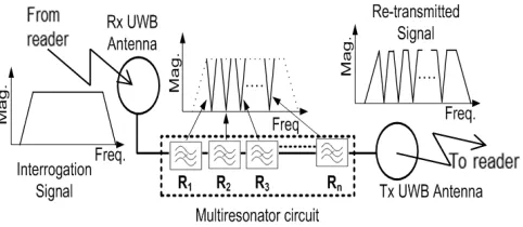
Figure 1. Configuration of a re-transmission based spectral signature encoded chipless RFID tag.
2. RETRANSMISSION BASED CHIPLESS RFID TAG
Retransmission based chipless RFID tags have two major components: i) a multiresonator circuit and ii) UWB antennas. Configuration of a retransmission based spectral signature encoded chipless RFID tag is shown in Figure 1. The multiresonator circuit encodes all the information for the tag and the two UWB antennas, one for reception (Rx) and the other for transmission (Tx), establishing communication link with the reader [13]. The Rx and Tx antennas are orthogonally polarized in order to minimize cross talk between the reader interrogation signal and the tag response signal [9].
3. DOUBLE BIT ENCODING USING A SINGLE MCSRR 3.1. Conventional CSRR and MCSRR
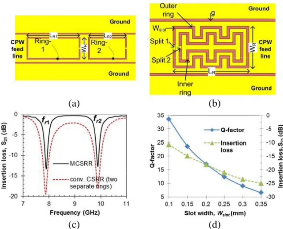
Complementary split ring resonators (CSRR) are widely used for highQband-stop filter applications [9]. In a conventional CSRR, there are two concentric rings where the splits of the two rings are located at two opposite sides of the resonator. Out of the two rings in the CSRR, the inner ring is used as a loading element for the outer ring, and both the rings collectively produce a single stop band [14, 15].
To produce two independently controllable resonances, two separate rings based CSRR can be considered as shown in Figure 2(a). The layout of the modified complementary split ring resonator (MCSRR) [14] that we have proposed is shown in Figure 2(b). In Figure 2(c), insertion loss results for the two separate rings based CSRR and MCSRR are presented. Comparing the two resonator configurations, besides occupying 56% less area, it is found that the proposed MCSRR also reduces the 3-dB resonance band (i.e., increases Qfactor) by more than 60%.
In order to understand the effect of slot width (Wslot) on the resonance bandwidth (inversely related to theQ-factor of the resonator), we carried out a parametric study of the proposed MCSRR. In Figure 2(d), results for parametric study of slot width (Wslot) onQ-factor and insertion loss performance of the MCSRR are presented. For the MCSRR, as Wslot increases, the Q-factor decreases whereas the insertion loss (S21) increases. This implies that the resonance bandwidth is lower (orQ-factor is higher)
whenWslot is smaller; however, for the current tag, slot widthWslot is set to a moderate value (0.15 mm) to ease fabrication complexity.
3.2. Detuning of Resonance
(a) (b)
(c) (d)
Figure 2. (a) Two separate rings based CSRR, (b) proposed dual-band MCSRR, (c) comparison of insertion loss results for the conventional CSRR and proposed MCSRR, and (d) study on the effect of slot width,Wslot on the Q-factor and insertion loss performance of the MCSRR.
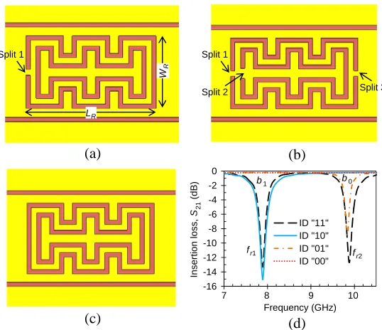
3.2.1. Encoding ‘11’
In the case of an MCSRR, out of the two stop-bands, the stop band at lower frequency is produced due to the resonance in the outer ring, and the stop band with higher frequency is produced due to resonance in the inner ring. While encoding the binary combination ‘11’, both the outer and inner rings are required to resonate and hence, for this condition, the layout of the MCSRR shown in Figure 2(b) is left unchanged. For encoding ‘11’, the lengths of ‘Split 1’ and ‘Split 2’ are set to 0.35 mm and 0.2 mm respectively.
3.2.2. Encoding ‘10’
The resonance frequency arising from outer ring is linked to MSB, and the resonance frequency arising from inner ring is linked to LSB. Thus, detuning of the resonance due to the inner ring is required to encode the binary combination ‘10’. Removing the split of the inner ring, as shown in Figure 3(a), detunes the corresponding resonance. However, detuning resonance of the inner ring changes the loading condition for the outer ring, and in the absence of the loading effect arising from the inner ring, the resonance frequency for the outer ring slightly shifts to higher frequency. Through reducing the length of ‘Split 1’ from 0.35 mm to 0.2 mm, this slight shift of resonance frequency has been mitigated.
3.2.3. Encoding ‘01’
Split 1 Split 1
Split 2 Split 3
LR
W
R
fr1 fr2
-16 -14 -12 -10 -8 -6 -4 -2 0
Insertion loss,
S
(dB)
ID "11" ID "10" ID "01" ID "00"
b1 b0
21
7 8 9 10
Frequency (GHz)
(a) (b)
(c) (d)
Figure 3. (a) Resonator layout for encoding ‘10’, (b) resonator layout for encoding ‘01’, (c) resonator layout for encoding ‘00’, and (d) insertion loss (S21) responses for an MCSRR configured to generate
all four combinations corresponding to the 2-bit binary word.
3.2.4. Encoding ‘00’
Encoding of binary combination ‘00’ requires detuning of the resonances due to both the inner and outer rings. When ‘Split 1’ and ‘Split 2’ are removed from the outer and inner rings respectively, as shown in Figure 3(c), both the resonances get detuned. Thus, while encoding ‘00’, no stop band is produced from the MCSRR.
For a single MCSRR, simulated insertion loss (S21) responses for four different binary combinations
(i.e. ‘11’, ‘10’, ‘01’ and ‘00’) are shown in Figure 3(d). The stop band due to the resonance in the outer ring occurs at frequencyfr1, and the stop band due to the resonance in the inner ring occurs at frequency
fr2, where,fr2> fr1. As can be seen from Figure 3(d), stop bands at bothfr1 andfr2can be controlled
independently, thus, a single MCSRR can be used for encoding and subsequent decoding of any arbitrary 2-bit binary data.
4. DESIGN OF A COMPACT MULTIRESONATOR
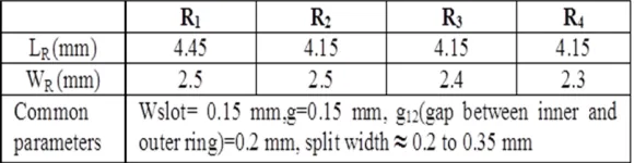
A multiresonator circuit with more than two-bit data capacity can be realized by cascading multiple MCSRRs with non-overlapping resonant frequencies. Cascading only four of the MCSRRs, an 8-bit multiresonator circuit is designed. A photograph of a sample 8-bit multiresonator circuit is shown in Figure 4(a). The circuit is based on CPW (Co-planar waveguide) configuration, and a substrate with only single sided metallization is used, thus, facilitates easy fabrication of the circuit. Here, a thin flexible substrate Taconic TLX-8 withεr = 2.55, tanδ = 0.0019 and thickness, h= 0.127 mm has been used. Physical parameters for the designed circuit are shown in Table 1. The designed circuit is capable of generating any 8-bit ID; however, for the purpose of demonstration, four arbitrary 8-bit codes are selected.
Measured insertion loss results (S21 magnitude) for the four 8-bit multiresonator circuits with
different IDs are shown in Figure 4(b). For the insertion loss results, the first four stop bands at fr1 o, fr2 o,fr3 o and fr4 o are originated due to the resonance of the outer rings of the resonatorsR1,R2,
R3 andR4 respectively, whereas, rest of the four stop bands atfr1 i,fr2 i,fr3 i andfr4 i are originated
due to the resonances of the inner rings of the same resonator group. Here, MSB (b7) and LSB (b0) of
R2 R4 R1
(a)
R3
fr1_o
fr2_o f fr3_o
fr4_o fr1_i
fr2_i
(b)
fr3_i fr4_i
ID='00000000' ID='11111111' ID='11000011' ID='00001111' -18
-16 -14 -12 -10 -8 -6 -4
S
Mag. (dB)21
Frequency (GHz)
6 7 8 9 10 11 12
Figure 4. (a) Photograph of a fabricated sample multiresonator circuit, (b) measured insertion loss (S21) responses for 8-bit multi-resonator (i.e., ID generator) circuits based on dual-band MCSRR.
Table 1. Physical parameters for the designed ID generation circuit (with reference to Figure 2(b) and Figure 4(a)).
As can be seen from Figure 4(b), when the circuit ID is ‘00000000’, no stop band is produced, and this response can be used as a reference for other IDs. For the circuit with ID = ‘11111111’, eight non-overlapping stop bands are produced where the measured S21 is below −9 dB for each of the stop
bands. When the ID of the circuit is changed to ‘11000011’, resonances due to the outer rings ofR3 and
R4 as well as resonances due to the inner rings ofR1 andR4 are effectively detuned, and hence, no stop
band is produced at those frequencies. When the circuit is configured for the ‘00001111’, resonances due to the outer rings of all four resonators are detuned, and hence, stop bands corresponding tob7–b4
bit positions do not appear in the insertion loss results. Therefore, for each of the attempted 8-bit IDs, measured insertion loss results correspond well to their designed binary information codes.
5. DESIGN OF UWB ANTENNA
Besides the multiresonator circuit, another integral part of the chipless tag, as shown in Figure 1, is two ultra wide band (UWB) planar antennas. As tag antennas, use of circular disk loaded monopole antenna has been widely reported in literature [16–20]. For the tag under investigation, two elliptical disk loaded UWB monopole antennas based on CPW configuration are designed, fabricated and tested. A photograph of a fabricated CPW monopole antenna is shown in Figure 5(a). Measured return loss (S11) for the antenna is presented in Figure 5(b), and the result shows that the designed antenna has
S11<−10 dB for 4.5 GHz to 11.5 GHz and covers the intended frequency band for the proposed chipless
tag. Measured co-polar and cross-polar gains for the designed antenna are presented in Figure 5(c). The antenna has a co-polar gain above 2 dBi in 0 degree azimuth direction for the intended frequency band. Measured cross-polar gain (also known as cross-polar isolation) for the antenna has an average value of
−14 dBi, where the cross-polar gain varies from−12 dBi to−18 dBi over the operating frequency band. MeasuredH- and E-plane radiation patterns for the fabricated antenna are presented in Figure 6. As expected for a monopole antenna, measured H-plane shows an omnidirectional pattern, and measured
6.5 7 7.5 8 8.5 9 9.5 10 10.5 11 11.5 Frequency (GHz)
Measured antenna gain
Antenna gain (co-polar) Antenna gain (cross-polar)
4 5 6 7 8 9 10 11
Frequency (GHz) d
Dx
Dy
hg wg
g
wf
(a) (b) (c)
-15 -10 -5 0 5
Antenna gain (dBi)
-30 -25 -20 -15 -10 -5 0
Return loss (dB)
Figure 5. Elliptical disk loaded CPW monopole antenna, (a) photograph, and (b) measured return loss, and (c) co-polar and cross-polar antenna gains. (Dx = 17.5 mm, Dy = 15.4 mm, hg = 10 mm,
d= 0.15 mm,wg = 30 mm, g= 0.15 mm, d= 0.15 mm,wf = 3.1 mm.).
-30 -30 -20 -20 -10 -10 0 dB 0 dB 90o 60o 30o 0o -30o -60o -90o -120o -150o 180o 150o 120o 7.0 GHz 9.0 GHz 11.0 GHz -30 -30 -20 -20 -10 -10 0 dB 0 dB 90o 60o 30o 0o -30o -60o -90o -120o -150o 180o 150o 120o 7.0 GHz 9.0 GHz 11.0 GHz (b) (a)
Figure 6. Measured radiation pattern for the elliptical disk loaded CPW monopole antenna. (a) H -plane and (b) E-plane.
Figure 7. Photograph of the integrated chipless RFID tag based on dual band MCSRR. (With the external SMA connectors, the tag size is 14 cm×8 cm, where, final tag size will be <6.5 cm×4 cm).
6. EXPERIMENTAL VALIDATION OF THE CHIPLESS TAG
(b) (a)
Figure 8. Experimental setup for testing of the tags, (a) schematic configuration and (b) photograph of the setup.
7 7.5 8 8.5 9 9.5 10 10.5 11
S
Mag. (dB)
21
ID-11111111 ID-00001111
ID-00000000 (Calibration)
b7 b6
b5
b4b3
b2 b1
b0
Frequency (GHz) -50
-45 -40 -35 -30 -25
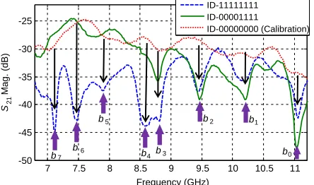
Figure 9. Measured tag responses for several differently coded 8-bit chipless RFID tags, where the tag to reader antenna distance (d) is set to 10 cm.
14.5 GHz with measured antenna gain of 14∼17 dBi, are used as reader transmitting (Tx) and receiving (Rx) antennas.
Measured transmission responses (S21 magnitude) between Tx and Rx reader antennas for several
8-bit integrated chipless tags with different IDs are presented in Figure 9. The tag with ID = ‘00000000’ is used as calibration tag. While decoding the state of particular data bit from measured tag response, occurrence of a local minima (i.e., abrupt change of slope) at the pre-specified resonance frequency position as well as large difference (i.e., 5 dB or more) in signal levels between tag under test and that for the calibration tag at the same frequency is considered as bit state ‘1’. If the two criteria are not fulfilled simultaneously, the bit state for the particular bit is considered as ‘0’.
As can be seen from measured results, the tag with ID = ‘11111111’, where all the resonators are tuned ‘ON’, produces eight nulls in the measuredS21response. For the tag with ID = ‘00001111’, nulls
are only produced for b3–b0 frequency positions, and no null is detected atb7 tob4 frequency positions.
While testing the integrated tags, the distance between the tag and the Tx/Rx antenna is set to 10 cm. If needed, longer reading range can be achieved by isolation (i.e., separation) between the Tx and Rx reader antennas, and also by increasing the Tx power level. Consistent measured results obtained from coded tags clearly demonstrate that the proposed tagging method based on MCSRR can be used for encoding and subsequent decoding of information bits for chipless RFID applications.
7. CONCLUSION
mechanisms have been utilized to allow encoding of two bits using a single resonator and thus enhancing the overall space efficiency and data density of the tag. Test results obtained for integrated proof-of-concept 8-bit chipless RFID tags confirm their functional validity. The proposed tag can be printed using conductive ink, or alternatively LASER diced and embedded (using hot stamping procedure), on flexible paper or plastic substrate for ultra-low cost RFID applications.
ACKNOWLEDGMENT
This work was supported in part by the Australian Research Council’s Linkage Project Grant (LP0989652: Printable Multi-bit RFID for Banknotes) and Securency Int. Pty Ltd. The authors also acknowledge the software support from CST MWS.
REFERENCES
1. Preradovic, S. and N. C. Karmakar, “Chipless RFID: Bar code of the future,” IEEE Microwave Magazine, Vol. 11, 87–97, 2010.
2. Mukherjee, S., “Chipless radio frequency identification by remote measurement of complex impedance,”European Conference on Wireless Technologies, 249–252, Munich, Germany, Oct. 8– 10, 2007.
3. Jang, H.-S., W.-G. Lim, K.-S. Oh, S.-M. Moon, and J.-W. Yu, “Design of low-cost chipless system using printable chipless tag with electromagnetic code,”IEEE Microwave and Wireless Components Letters, Vol. 20, 640–642, 2010.
4. Blischak, A. and M. Manteghi, “Pole residue techniques for chipless RFID detection,” IEEE Antennas and Propagation Society International Symposium, 1–4, Jun. 1–5, 2009.
5. Islam, M. A., Y. Yap, N. C. Karmakar, and A. Azad, “Compact printable orientation independent chipless RFID tag,” Progress In Electromagnetics Research C, Vol. 33, 55–66, 2012.
6. Shao, B., Q. Chen, R. Liu, and L.-R. Zheng, “Design of fully printable and configurable chipless RFID tag on flexible substrate,”Microwave and Optical Technology Letters, Vol. 54, 226–230, 2012. 7. Vena, A., E. Perret, and S. Tedjini, “A fully printable chipless RFID tag with detuning correction
technique,”IEEE Microwave and Wireless Components Letters, Vol. 22, 209–211, 2012.
8. Preradovic, S. and N. C. Karmakar, “Design of chipless RFID tag for operation on flexible laminates,”IEEE Antennas and Wireless Propagation Letters, Vol. 9, 207–210, 2010.
9. Preradovic, S., I. Balbin, N. C. Karmakar, and G. F. Swiegers, “Multiresonator-based chipless RFID system for low-cost item tracking,”IEEE Transactions on Microwave Theory and Techniques, Vol. 57, 1411–1419, 2009.
10. Balbin, I. and N. Karmakar, “ovel chipless RFID tag for conveyor belt tracking using multi-resonant dipole antenna,” 39th European Microwave Conference, 1109–1112, Rome, Italy, Sep. 29–Oct. 1, 2009.
11. Nijas, C. M., R. Dinesh, U. Deepak, A. Rasheed, S. Mridula, K. Vasudevan, et al., “Chipless RFID tag using multiple microstrip open stub resonators,” IEEE Transactions on Antennas and Propagation, Vol. 60, 4429–4432, 2012.
12. Preradovic, S., “Chipless RFID system for barcode replacement,” Ph.D. Thesis, Department of Electrical and Computer Systems Engineering, Monash University, Melbourne, 2009.
13. Girbau, D., J. Lorenzo, A. Lazaro, C. Ferrater, and R. Villarino, “Frequency-coded chipless RFID tag based on dual-band resonators,” IEEE Antennas and Wireless Propagation Letters, Vol. 11, 126–128, 2012.
14. Al-Nuaimi, M. K. T. and W. G. Whittow, “Compact microstrip band stop filter using SRR and CSSR: Design, simulation and results,”Proceedings of the Fourth European Conference on Antennas and Propagation (EuCAP), 1–5, Apr. 12–16, 2010.
16. Lee, C.-M., T. C. Yo, C.-H. Luo, C.-H. Tu, and Y.-Z. Juang, “Broadband disk monopole antenna with a circular CPW-feeding line,” 2007 IEEE Antennas and Propagation Society International Symposium, 773–776, 2007.
17. Lin, C.-C. and H.-R. Chuang, “A 3–12 GHz UWB planar triangular monopole antenna with ridged ground-plane,”Progress In Electromagnetics Research, Vol. 83, 307–321, 2008.
18. Liang, J., L. Guo, C. C. Chiau, and X. Chen, “CPW-fed circular disc monopole antenna for UWB applications,” IEEE International Workshop on Antenna Technology: Small Antennas and Novel Metamaterials, IWAT 2005, 505–508, 2005.
19. Liang, J., L. Guo, C. C. Chiau, X. Chen, and C. G. Parini, “Study of CPW-fed circular disc monopole antenna for ultra wideband applications,” IEE Proceedings on Microwaves, Antennas and Propagation, 520–526, 2005.