A LOW POWER LEVEL SHIFTER USING POWER
GATING TECHNIQUE FOR SOC APPLICATIONS
Arun.P
1
, K. Suganthi
2
1
Research Scholar in Mech. Deptt, SRM University, Tamilnadu
2
Asst. Professor, Deptt. Of ECE, SRM University, Tamilnadu (India)
ABSTRACT
A low-power level shifter (LS) using power gating technique is proposed for logic voltage shifting from
near/sub-threshold to above-near/sub-threshold voltage domain. Level shifter allow for effective interfacing between voltage domains
supplied by different voltage level. Usually conventional level shifter which can shift any voltage level signal to a
desired higher level with low leakage current. The new circuit combines the multi-threshold CMOS technique
along with topological modifications to provide a wide voltage conversion range with limited static power ,
dynamic power and total energy per transition . When implemented in a 45-nm technology process the proposed
design converts 250mV input signals to 1V output signal with lesser dynamic power, static power and total energy
per consumption while maintaining operational frequencies above 1MHz.
Keywords: Sub Level Shifter, Multi Threshold CMOS Technique, Sub-Threshold.
I INTRODUCTION
The Deviation from constant field scaling due to the non-scaling parameters of the MOS transistors (thermal
voltage, silicon energy band gap, and source/drain doping levels) leads to an increase in the power consumption
and power density with each new technology [1] [3]. The increased power dissipation degrades the reliability,
increase the cost of the packaging and cooling system, and lower the battery lifetime in electronic device. The
multi-supply voltage domain technique [3], based on partitioning the design into separate voltage domains (or
voltage islands) with each domain operating at a proper power supply voltage level is preferred depending on its
timing requirement. Time-critical domain runs at higher power supply voltage (VDDH) to enhance the
performance, whereas noncritical sections work at lower power supply voltage (VDDL) to enhance power
efficiency. Power consumption is the top concerns of VLSI circuit design. To solve this power dissipation
problem, many researchers have proposed ideas differing from the device level to the architectural level and above.
However, there is no universal way to avoid tradeoffs between delay, power, and area, and thus, designers are in
demand to choose appropriate techniques that satisfy application and product needs. Power consumption of
CMOS consists of dynamic and static components. Dynamic power consumption is when transistors are switching
leakage power is the increase of sub-threshold leakage power. When technology scales down, supply voltage also
scales down simultaneously. This paper deals with a low-power LS using power gating technique designed to
convert near-threshold or sub-threshold voltages to above-threshold voltage levels. The basic strategy of power
gating is to provide two power modes a standby mode and an active mode. The goal is to switch between these
modes at the appropriate time and in the appropriate manner to maximize power savings while minimizing the
impact to performance. When implemented with the 45-nm GPDK technology, the new design successfully
converts input voltages as low as 0.250 V to the 1-V output with a dynamic power dissipation of 491.84nW in
active mode and 7.3nW in standby mode. The Static power in active and standby mode obtained as 141.1802pW
and 3.485pW respectively. The total energy per transition obtained as 147.4fJ and 0.483fJ in active and standby
mode respectively.
II
OPERATING PRINCIPLES
2.1 Conventional Level Shifter
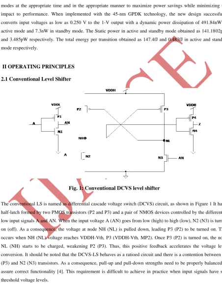
Fig. 1: Conventional DCVS level shifter
The conventional LS is named as differential cascade voltage switch (DCVS) circuit, as shown in Figure 1 It has a
half-latch formed by two PMOS transistors (P2 and P3) and a pair of NMOS devices controlled by the differential
low input signals A and AN. When the input voltage A (AN) goes from low (high) to high (low), N2 (N3) is turned
on (off). As a consequence, the voltage at node NH (NL) is pulled down, leading P3 (P2) to be turned on. This
occurs when NH (NL) voltage reaches VDDH-Vth, P3 (VDDH-Vth, MP2). Once P3 (P2) is turned on, the node
NL (NH) starts to be charged, weakening P2 (P3). Thus, this positive feedback accelerates the voltage level
conversion. It should be noted that the DCVS-LS behaves as a ratioed circuit and there is a contention between P2
(P3) and N2 (N3) transistors. As a consequence, pull-up and pull-down strengths need to be properly balanced to
assure correct functionality [4]. This requirement is difficult to achieve in practice when input signals have sub
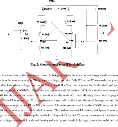
2.2 Conventional Type II
Figure 2 shows that the circuit consists of an input inverter stage, a main voltage conversion stage, and an output
inverting buffer.
Fig. 2: Conventional type II level shifter
A high to low transition of the main input causes P4 being turned on. Its drain current brings the diode-connected
P6 device into the saturation region. This creates a voltage drop (i.e., Vth, P6) across P6 terminals that produce a
correspondent bulk source voltage drop on P4. Due to the bulk effect, this increases the P4 threshold voltage. The
reduced voltage level (VDDH-Vth, P6) on the source terminal of P4 limits its VGS, thus further weakening the P4
action. All the above effects reduce the contention on the node NH, thus allowing faster discharging to be
achieved. When P4 is turned on, P5 is consequently turned off. In this case, the small leakage current flowing
through P5 is not enough to turn P7 on. For this reason, P5 results power gated from the VDDH power rail, leading
to a significant reduction in its sub-threshold current. The diode-connected P7 device participates in minimizing
the leakage current, also by increasing the threshold voltage of P5. In fact P7 causes the source of transistor M5 to
be at lower voltage than the bulk node and thereby reduces the sub threshold leakage current due to the bulk effect.
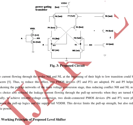
III PROPOSED LEVEL SHIFTER
3.1 Design
Figure 3 shows the architecture of proposed level shifter. The new power gated level shifter [1] is described in this
section. Power gating uses low-leakage PMOS transistors as header switches to shut off power supplies to parts of
a design in standby. Here high-Vt transistors are used for power gating.This level shifter uses a multi VTH CMOS
while using this technique, the most important ones being power gate size and power gate leakage. The power gate
size must be selected to handle the amount of switching current at any given time. The gate must be bigger such
that there is no measurable voltage (IR) drop due to the gate. Since power gates are made of active transistors,
leakage reduction is an important consideration to maximize power savings. As shown in Figure 3, the circuit
consists of an input inverter stage, a main voltage conversion stage and an output inverting buffer and power gating
transistor. To increase the strength of the pull-down network of the main voltage conversion stage, it was also
designed by using HVT transistors.
Fig. 3: Proposed Circuit
The current flowing through the nodes NH and NL at the beginning of their high to low transition could be of
concern [5]. Thus, to reduce this effect, two PMOS devices (P2 and P3) are adopted. P4 and P5 helped in
weakening the pull-up networks of the main voltage conversion stage, thus reducing conflict NH and NL nodes.
This choice also reduced the leakage current flowing through the pull-up networks when they are turned OFF.
Finally, to achieve reliable voltage conversion, two diode-connected PMOS devices (P6 and P7) were placed
between the pull-up logics and the supply rail VDDH. This device limits the pull-up strength, but also reduces
static power.
3.2 Working Principle of Proposed Level Shifter
Power gating is a technique used in integrated circuit design to reduce power consumption, by shutting off
the current to blocks of the circuit that are not in use. In addition to reducing stand-by or leakage power a high to
low transition of the main input causes P4 being turned ON. Its drain current brings the diode-connected P6 device
into the saturation region. This creates a voltage drop across P6 terminal that produce a bulk source voltage drop
on P4. Due to this bulk effect, there is increase in the P4 threshold voltage and the reduced voltage level
(VDDHVTH, P6) on the source terminal of P4 limits its VGS, thus further weakening the P4 action. When P4 is
turned ON, P5 is turned off. In this case, the small leakage current flowing through P5 is not enough to turn P7
sub-threshold current. The diode connected P7 device minimizes the leakage current, also by increasing the
threshold voltage of P5. In fact, P7 causes the source of transistor P5 to be at lower voltage than the bulk node and
thereby reduces the sub-threshold leakage current due to the bulk effect. This significantly differs from those
adopted in other LS designs that implemented diode connected transistors [7]. Since P6 limits the output range of
the main conversion stage to [0 V, VDDH – VTP], an output inverter is connected to node NH, to assure a required
conversion. The pull down of such an inverter uses a P8, P9 and N4 device, whereas its pull-up is designed by
exploiting PMOS transistors stack, thus limiting the leakage current flowing through the pull-up network of the
output inverter, when NH is high. Opposite and substantial threshold voltage variations on P6 and P8-P9 could,
cause the latter transistors to go in weak inversion, thus increasing the static power dissipation. Now power gated
transistor is placed in series with P6, P7, P8 and power supply. A power gating technique is used for efficient
power management. In the active mode, the input to power gated (hvt) is set low and power gated transistor (hvt) is
turned ON. Since their on-resistances is small, the supply voltage almost function as real power line. In the standby
mode, the input to power gated (hvt) is set high, power gated transistor (hvt) turned OFF and decreasing the power
dissipation.
IV RESULTS AND ANALYSIS
Using 45nm Cadence GPDK technology the new level shifter is compared to the conventional level shifter II for
dynamic, static power and total energy per transition. The availability of high efficiency power supplies and the
availability of a multi-VTH CMOS technology are the important factors affecting the optimum supply voltages in a
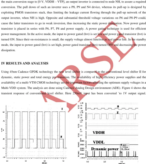
Multi-VDD system. The analysis are done using Cadence Analog Design environment (ADE). Figure 4 shows the
transient response of conventional level shifter. Here 250mV input has been converted `to 1V output signal.
Fig 4: Transient Response of Conventional LS II Fig Fig 5: Dynamic Power of Conventional LS II
Figure 5 shows the dynamic power dissipation of conventional level shifter II. An input pulse of 250mV is given
and an output pulse of 1V is obtained. The dynamic power dissipation obtained was 595.99nW. The static power
provided in this case was 1V. The total energy per transition for conventional level shifter II obtained as 159.3fJ.
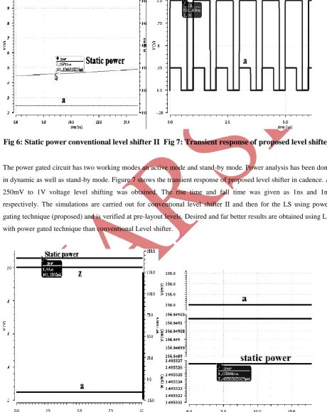
Fig 6: Static power conventional level shifter II Fig 7: Transient response of proposed level shifter
The power gated circuit has two working modes an active mode and stand-by mode. Power analysis has been done
in dynamic as well as stand-by mode. Figure 7 shows the transient response of proposed level shifter in cadence. A
250mV to 1V voltage level shifting was obtained. The rise time and fall time was given as 1ns and 1ns
respectively. The simulations are carried out for conventional level shifter II and then for the LS using power
gating technique (proposed) and is verified at pre-layout levels. Desired and far better results are obtained using LS
with power gated technique than conventional Level shifter.
Figure 8 shows the static power dissipation for the proposed level shifter obtained as 141.1802pW in active mode.
The static power in standby mode of proposed level shifter was found to be 3.48pW and shown in fig: 9.
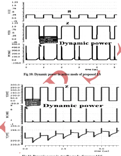
Fig 10: Dynamic power in active mode of proposed LS
Fig 11: Dynamic power in standby mode of proposed LS
Figure 10 shows the dynamic power of proposed LS in active mode and was obtained as 491.841nW. The dynamic
power at standby mode of proposed LS was obtained as 7.3nW. It is observed that our approach gave far better
results for dynamic power dissipation and total energy per transition and reduction of static power in standby mode
Fig 12: Layout of the proposed circuit
Figure 12 here illustrate the physical design of the proposed level shifter.
DESIGN TECH VDDH
(V) VDDL (mV) INPUT (mV) OUTPUT (V) DYNAMIC POWER (nW) STATIC POWER (pW) TOTAL ENERGY/ TRANSITION (fJ) Conventional
type II 45nm 1 250 250 1 595.994 141.1806 159.3
Proposed (Active
mode)
45nm 1 250 250 1 491.841 141.1802 147.4
Proposed (Standby mode)
45nm 1 250 250 1 7.301 3.4855 0.483
TABLE 1: EXPERIMENTAL RESULTS AND COMPARISON
V CONCLUSION
A new low-power LS has been proposed suitable for logic voltage shifting from near/sub-threshold to above
threshold domain with reduced dynamic, static power dissipation and total energy per transition. The circuit when
used for sub-threshold to above threshold voltage conversion, exhibits the lowest static power and energy
consumption with respect to previous proposed LSs that used similar design parameters. Moreover, even though the
new designed LS is optimized for low power consumption, it also and supports a wide voltage conversion range.
REFERENCES
[1] Marco Lanuzza and Stefania perri. “Low power level shifter for multi supply voltage designs”. IEEE Trans.
Very Large Scale Integr. (VLSI) Syst. 2012; 59(12): 922-926
[2] P Corsonello, M Lanuzza, and S Perri. “Gate-level body biasing technique for high-speed sub-threshold CMOS
logic gates”. Int. J. Circuit Theory Appl. 2012.
[3] JC Chi, HH Lee, SH Tsai, and MC Chi. “Gate level multiple supply voltage assignment algorithm for power
optimization under timing constraint”. IEEE Trans. Very Large Scale Integr. (VLSI) Syst. 2007; 15(6):
637-648.
[4] TH Chen, J Chen, and LT Clark. “Subthreshold to above threshold level shifter design”. J. Low Power
Electron.2006; 2(2): 251-258.
[5] Y.-S. Lin and D. M. Sylvester, “Single stage static level shifter design for subthreshold to I/O voltage
conversion,” in Proc. IEEE/ACM 13thISLPED, 2008, pp. 197–200.
[6] S. N. Wooters, B. H. Calhoun, and T. N. Blalock, “An energy-efficient subthreshold level converter in 130-nm CMOS,” IEEE Trans. CircuitsSyst. II, Exp. Briefs, vol. 57, no. 4, pp. 290–294, Apr. 2010.
[7] Chavan and E. MacDonald, “Ultra low voltage level shifters to interface sub and super threshold reconfigurable