Modular Hardware Architecture for Somewhat
Homomorphic Function Evaluation
Sujoy Sinha Roy1, Kimmo J¨arvinen1, Frederik Vercauteren1, Vassil Dimitrov2,
and Ingrid Verbauwhede1
1 KU Leuven ESAT/COSIC and iMinds
Kasteelpark Arenberg 10, Bus 2452, B-3001 Leuven-Heverlee, Belgium [email protected]
2
The University of Calgary, Canada and Computer Modelling Group, Ltd. 2500 University Dr. NW, Calgary, AB, Canada, T2N 1N4
Abstract. We present a hardware architecture for all building blocks re-quired in polynomial ring based fully homomorphic schemes and use it to instantiate the somewhat homomorphic encryption scheme YASHE. Our implementation is the first FPGA implementation that is designed for evaluating functions on homomorphically encrypted data (up to a certain multiplicative depth) and we illustrate this capability by evaluating the SIMON-64/128 block cipher in the encrypted domain. Our implemen-tation provides a fast polynomial operations unit using CRT and NTT for multiplication combined with an optimized memory access scheme; a fast Barrett like polynomial reduction method; an efficient divide and round unit required in the multiplication of ciphertexts and an efficient CRT unit. These building blocks are integrated in an instruction-set co-processor to execute YASHE, which can be controlled by a computer for evaluating arbitrary functions (up to the multiplicative depth 44 and 128-bit security level). Our architecture was compiled for a single Virtex-7 XCVirtex-7V1140T FPGA, where it consumes 23 % of registers, 53 % of LUTs, 53 % of DSP slices, and 38 % of BlockRAM memory. The implementation evaluates SIMON-64/128 in approximately 171.3 s (at 143 MHz) and it processes 2048 ciphertexts at once giving a relative time of only 83.6 ms per block. This is 24.5 times faster than the leading software implemen-tation on a 4-core Intel Core-i7 processor running at 3.4 GHz.
Keywords.Fully homomorphic encryption, YASHE, FPGA, NTT, CRT
1
Introduction
The concept of fully homomorphic encryption (FHE) was introduced by Rivest, Adleman, and Dertouzos [34] already in 1978 and allows evaluating arbitrary functions on encrypted data. Constructing FHE schemes proved to be a dif-ficult problem that remained unsolved until 2009 when Gentry [22] proposed
c
IACR 2015. This article is a minor revision of the version published by Springer-Verlag available at DOI: 10.1007/978-3-662-48324-4 9.
the first FHE scheme by using ideal lattices. Despite its groundbreaking na-ture, Gentry’s proposal did not provide a practical solution because of its low performance. Since then, many researchers have followed the blueprints set out by Gentry’s proposal with an objective to improve the performance of FHE [6, 7, 14, 17, 20, 24, 25, 32]. Most schemes are either based on (ring) learning with errors ((R)LWE) or N-th degree truncated polynomial ring (NTRU) and thus manipulate elements in modular polynomial rings, or on the approximate great-est common divisor (GCD) problem which manipulates very large integers. In this paper, we focus on the former category. Although major advances have been made, we are still lacking FHE schemes with performance levels that would allow large-scale practical use. Software implementations still require minutes or hours to evaluate even rather simple functions. For instance, evaluating the lightweight block cipher SIMON-64/128 [4] requires 4193 s (an hour and 10 minutes) on a 4-core Intel Core-i7 processor [29]. Note that homomorphic evaluation of a block cipher decryption is required to reduce the network communication to the data size following the proposal in [32]: data is encrypted with a block cipher by the user and then the server decrypts the ciphertext by evaluating the block cipher homomorphically by using a homomorhic encryption of the key. If FHE could achieve performance levels that would permit large-scale practical use, it would have a drastic effect on cloud computing: users could outsource computations to the cloud without the need to trust service providers and their mechanisms for protecting users’ data from outsiders.
accelera-tion of FHE schemes. So far, no results are available on hardware acceleraaccelera-tion of function evaluation on homomorphically encrypted data, although this is the most crucial part of FHE schemes in application scenarios.
We present the first efficient FPGA implementation of the building blocks required in modular polynomial ring based fully homomorphic schemes such as those built on RLWE [8] or NTRU [30]. These building blocks are sufficiently generic to allow implementation of such FHE schemes, and to illustrate this, we integrate these building blocks into a coprocessor architecture that can eval-uate functions encrypted with the FHE scheme called Yet Another Somewhat Homomorphic Encryption (YASHE) [6]. To the best of our knowledge, it is the first FPGA implementation that supports function evaluation of homomor-phically encrypted data. We use several standard optimization techniques such as the Chinese remainder theorem (CRT) representation, the number theoretic transformation (NTT) and fast modular polynomial reduction, but introduce several optimizations specific for the FPGA platform such as a specific mem-ory access scheme for the NTT. We compile the architecture for Xilinx Virtex-7 XC7V1140T FPGA. We show that a single FPGA achieves speedups up to factor 24.5 in executing SIMON-64/128 compared to a corresponding software imple-mentation running on a 4-core Intel Core i7 processor from [29].
The paper is structured as follows. Section 2 describes the mathematical objects underlying FHE and recaps the YASHE scheme. Section 3 contains a high level description of known optimization techniques to speed-up computations in modular polynomial rings and describes how we represent polynomials using CRT in order to parallelize computations. We present our hardware architecture for the primitives of YASHE in Section 4. We provide implementation results on a Xilinx Virtex-7 FPGA and compare them to existing software results in Section 5. We end with conclusions and future work in Section 6.
2
System Setup
2.1 Modular Polynomial Rings
The FHE schemes based on RLWE [8] or NTRU [30] compute in modular poly-nomial rings of the form R = Z[x]/(f(x)) where f(x) is a monic irreducible polynomial of degree n. A very popular choice is to take f(x) = xn+ 1 with n = 2k, since this is compatible with a 2n-degree NTT and reduction modulo f(x) comes for free due to the NTT. However, we put no restriction on f(x), which allows us to deal with any cyclotomic polynomialΦd(x) and thus to utilize single instruction multiple data (SIMD) operations [36, 37].
For an integerq, we denote byRq =R/qR, i.e. the polynomial ring where the
coefficients are reduced moduloq. The plaintext space in FHE schemes typically will be R2, and if one wants to utilize SIMD operations the polynomial f(x)
it results in only one irreducible factor modulo 2. In most polynomial ring based FHE schemes, a ciphertext consists of one or two elements inRq. However, not
all operations take place in the ringRq; sometimes (see below for an illustration
with YASHE) one is required to temporarily work in R itself before mapping down intoRq again using (typically) a divide and round operation.
2.2 YASHE
The YASHE scheme was introduced by Bos et al. in [6] in 2013. The scheme works in the ringR=Z[x]/(f(x)), withf(x) =Φd(x) thed-th cyclotomic polynomial.
The plaintext space is chosen as Rt for some small t (typically t = 2) and a ciphertext consists of only one element in the ring Rq for a large integer q. The main security parameters of the scheme are the degree of f(x) and the size of
q. We note that qis not required to be a prime and can be chosen as a product of small primes to speed-up computations (see Section 3). To define the YASHE scheme we also require two probability distributions defined onR, namelyχkey
andχerr. In practice one often takesχerrto be a discrete Gaussian distribution,
whereas χkey can be simply sampling each coefficient from a narrow set like {−1,0,1}. Given an elementa∈Rq and a basew, we can writeain basewby splicing each of its coefficients, i.e. writea =Pui=0aiwi with each ai ∈ R and
coefficients in (−w/2, w/2] andu=blogw(q)c. Decomposing an elementa∈Rq
into its base w components (ai)u
i=0 is denoted by WordDecompw,q(a). For an
elementa∈Rq, we definePowersOfw,q(a) = (awi)ui=0, the vector that consists of
the elementascaled by the different powers ofw. Both operations can be used to provide an alternative description of multiplication inRq, namely:
hWordDecompw,q(a),PowersOfw,q(b)i=a·bmodq .
The advantage of the above expression is that the first vector contains small elements, which limits error expansion in the homomorphic multiplication.
An FHE scheme is an augemented encryption scheme that defines two ad-ditional operations on ciphertexts, YASHE.Add and YASHE.Mult that result in a ciphertext encrypting the sum (respectively the product) of the underlying plaintexts. The YASHE scheme is then defined as follows (full details can be found in the original paper [6]).
– YASHE.ParamsGen(λ): For security parameterλ, choose a polynomialΦd(x), moduliqandtand distributionsχerrandχkeyattaining security levelλ. Also choose basewand return the system parameters (Φd(x), q, t, χerr, χkey, w).
– YASHE.KeyGen(Φd(x), q, t, χerr, χkey, w): Sample f0, g ← χkey and set f = (tf0+ 1) ∈ Rq. If f is not invertible in Rq choose a new f0. Define h =
tgf−1∈Rq. Sample two vectorse,sofu+1 elements fromχerrand compute
γ=PowersOfw,q(f) +e+hs∈Ruq+1 and output (pk, sk, evk) = (h, f, γ).
– YASHE.Encrypt(h, m): To encrypt a messagem∈Rtsamples, e←χerr and output the ciphertextc=∆·m+e+sh∈Rq with∆=bq/tc.
– YASHE.Decrypt(f, c): Recovermasm=bt
q·[f·c]qe ∈Rtwith [·]q reduction
Input: Polynomiala(x)∈Zq[x] of degreeN−1 andN-th primitive rootωN∈Zqof unity
Output: PolynomialA(x)∈Zq[x] = NTT(a) 1 begin
2 A←BitReverse(a);
3 form= 2toN bym= 2mdo
4 ωm←ωNN/m;
5 ω←1 ;
6 forj= 0tom/2−1do
7 fork= 0toN−1bymdo
8 t←ω·A[k+j+m/2] ;
9 u←A[k+j] ;
10 A[k+j]←u+t;
11 A[k+j+m/2]←u−t;
12 ω←ω·ωm;
Algorithm 1: Iterative NTT [13]
– YASHE.Add(c1, c2): Returnc1+c2∈Rq.
– YASHE.KeySwitch(c, evk): ReturnhWordDecompw,q(c), evki ∈Rq
– YASHE.Mult(c1, c2, evk): Return c = YASHE.KeySwitch(c0, evk) with c0 =
bt
qc1c2e ∈Rq.
YASHE Paramater Set: We use the parameter set Set-III from [29] that sup-ports homomorphic evaluations of SIMON-64/128; in particulard= 65535 (and thus the degree of f(x) is 32768 = 215), log
2(q) = 1228 and χerr a discrete
Gaussian distribution with parameterσ= 8. The paper [29] claims that this set has security level 128-bits, but this is an underestimate due to a small error in the security derivation. We chose SIMON because it has a smaller multiplica-tive depth (e.g. AES), and because it offers direct comparability to the existing software implementation [29].
3
High Level Optimizations
To efficiently implement YASHE we have to analyze the two main operations in detail, namely homomorphic addition and homomorphic multiplication. Homo-morphic addition is easy to deal with since this simply corresponds to polynomial addition in Rq. Homomorphic multiplication is much more involved and is the main focus of this paper. As can be seen from the definition of YASHE.Multin Section 2.2, to multiply two ciphertexts c1 and c2 one first needs to compute
c1·c2over the integers, then scale by t/qand round, before mapping back into
the ringRq. The fact that one first has to compute the result over the integers
(to allow for the scaling and rounding) has a major influence on how elements ofRq are represented and on how the multiplication has to be computed.
First we will consider polynomial multiplication in Rq where the modulus f(x) is an arbitrary polynomial of degree n. Since each element inRq therefore
can be represented as a polynomial of degree n−1, the resulting product will have degree 2n−2. As such we choose the smallest N = 2k > 2n−2, and
the N-fold NTT (see Alg. 1). The NTT requires the N-th roots of unity to exist in Zq, so we either choose qa prime withq≡1 modN or q a product of
small primesqiwith eachqi≡1 modN. It is the latter choice that will be used
throughout this paper.
The product of two elementsa, b∈Rq is then computed in two steps: firstly, the product modulo xN −1 (note that there will be no reduction, since the degree of the product is small enough) is computed using two NTT’s,Npointwise multiplications moduloqand then finally, one inverse NTT. To recover the result inRq, we need a reduction modulof(x). For generalf(x) this reduction does not
come for free (unlike the choicef(x) =xn+1) and for the parameters used in the
YASHE scheme the polynomial f(x) is in fact quite dense (although almost all coefficients are±1). We have to consider generalf(x) because the most obvious choicef(x) =xn+ 1 does not allow SIMD operations, sincef(x) mod 2 has only
one irreducible factor. The polynomial Φd(x) from the YASHE parameter set splits modulo 2 in 2048 different irreducible polynomials, which implies that we can work on 2048 bits in parallel using the SIMD method first outlined in [36].
To speed-up the reduction modulof(x) we rely on a polynomial version of Barrett reduction [21], where one precomputes the inverse of xnf(1/x)
mod-ulo xn. The quotient and remainder can then be recovered at the cost of two
polynomial multiplications.
Note that the multiplication ofc1 andc2 in YASHE.Mult is performed over
integers. To get the benefit of NTT based polynomial multiplication, we perform this multiplication in a ringRQ where Qis a sufficiently large modulus of size ∼2 logqsuch that the coefficients of the result polynomial are inZ.
CRT Representation of Polynomials: In the cryptosystems based on the RLWE problem, computations are performed on the polynomials of a ring Rq. The reported FPGA-based architectures [3, 33, 35] of such cryptosystems use BRAM slices to store the polynomials and use arithmetic components made up of DSP multipliers and LUTs. The biggest challenge while designing a homo-morphic processor is the complexity of computation. During a homohomo-morphic operation, computations are performed on polynomials of degree 215 or 216 and coefficients of size∼1,200 or∼2,500 bits. If we use a bit-parallel coefficient mul-tiplier, then a 2,500×2,500-bit multiplier will not only result in an enormous area, but will also result in a very low operating frequency. On the other side, a word-serial multiplier is too slow for homomorphic computations.
To tackle the problem of long integer arithmetic, we take inspiration from the application of the CRT in the RSA cryptosystems. We choose the moduliq
and Qas products of many small prime moduli qi, such thatq =Ql0−1qi and
Q=QL0−1qi, wherel < L. We map any long integer operation moduloqor Q
into small computations moduliqi, and apply CRT whenever a reverse mapping
is required. We use the term small residue to represent coefficients modulo qi
Parallel Processing: Beside making the long integer operations easy, such small-residue representation of the coefficients have a tremendous effect on the computation time. Since the computations in the small-residue representations are independent of each other, we can exploit this parallelism and speedup the computations using several parallel cores.
The size of the moduliqiis an important design decision and depends on the
underlying platform. We use the largest Xilinx Virtex-7 FPGA XC7VX1140T
to implement our homomorphic processor and tune the design decisions accord-ingly. The FPGA has 3,360 25×18-bit DSP multipliers [1]. One could implement a slightly larger multiplier by combining DSP multipliers with LUTs. For the set of moduli, we choose in total 84 primes (hence l = 41 and L= 84) of size 30 bits, (the primes from 1008795649 onwards) satisfying qi ≡1 modN. The reasons for selecting only 30-bit of primes are: 1) there are sufficiently many primes of size 30-bit to compose 1,228-bitq and 2,517-bitQ, 2) the data-paths for performing computations moduloqibecome symmetric, and 3) the basic com-putation blocks, such as adders and multipliers of size 30-bit can be implemented efficiently using the available DSP slices and a few LUTs.
4
Architecture
We propose an architecture (Fig. 1) to perform the operations in the YASHE scheme. The central part of the architecture is an FPGA based accelerator that works as a coprocessor of a computer and executes the computationally intensive operations. We call this coprocessor the HE-coprocessor. The HE-coprocessor supports the following operations: NTT of a polynomial, coefficient wise
addi-q0
,
qh
,
. . .
moduli
DRU
DRU DRU
DRU DRU
DRU
h
−1
q
,
q
1
h+1
,. . .
qh−1
. . .,
FSMs for NTT, Coefficient−wise Addition, Subtraction,
and Multiplication of Polynomials, CRT, and Division−Round HE−Coprocessor FPGA
DRU: Division and Rounding Unit CRTU: CRT Unit
PAU: Polynomial Arithmetic Unit
External Memory
Processor PAU + CRTU
Processor 1 PAU + CRTU
Processor 0 PAU + CRTU
moduli moduli
Computer (Master Mode) External Memory Control
Instruction
tion/subtraction/multiplication of two polynomials, computation of the residues using the CRT, computation of the coefficients moduloQfrom the residues, and the scaling of the coefficients. The external memory in this architecture is imple-mented using high-speed RAMs and is used to store the polynomials during a homomorphic computation. The computer in Fig. 1 works in master-mode and instructs the HE-coprocessor and the controller of the external memory. Since the execution of the homomorphic scheme is controlled by a software program in the computer, a level of flexibility to implement other homomorphic schemes based on a similar set of elementary operations is offered.
The HE-coprocessor comprises of three main components: the polynomial arithmetic unit (PAU), the CRT unit (CRTU), and the division and rounding unit (DRU). We do not implement the discrete Gaussian sampling in the HE-coprocessor as sampling is required only during an encryption, which is a less frequent operation. Since the samples from a narrow discrete Gaussian distri-bution can be generated very efficiently using lookup tables in software [11], we use the master-computer (Fig. 1) for this purpose.
4.1 Polynomial Arithmetic Unit
To exploit the parallelism provided by the small-residue representation of the polynomials, the PAU has h parallel processors to perform computations on
hresidue polynomials simultaneously. We call this horizontal parallelism. Since the targeted FPGA does not provide sufficient resources to process all the small-residue polynomials in parallel, we design the processors in a generic way such that a processor can be time-shared by a group ofdL/heprime moduli. To add an additional degree of acceleration, we add v parallel cores in each processor. We call this vertical parallelism. The cores in a processor are connected to a group of BRAMs through a switching matrix.
Optimization in the Routing: During an NTT computation (Alg. 1), coeffi-cients are fetched from the memory and then butterfly operations are performed on the coefficients. Let us assume that a residue polynomial ofN = 216
coeffi-cients is stored inbBRAMs and then processed usingv butterfly cores. Ifv is a divisor ofb, then we can split the NTT computation in equal parts among thev
In the FPGA, fetching data from memory locations at a relative distance of 215
will result in a long routing, and thus could drastically reduce the frequency. To address these two technical challenges, we have developed a memory access scheme by analysing the address generation during different iterations of the loops in the NTT (Alg. 1) We segment the set of b BRAMs into b/v groups. The read ports of a group are accessed by only one butterfly core. Thisdedicated read prevents any sort of conflict during the memory read operations. Moreover, in the FPGA the group of BRAMs can be placed close to the corresponding butterfly core and thus the routing complexity can be reduced.
We describe the proposed memory access scheme during an execution of the NTT by parallel cores in Alg. 2. The module butterfly-core performs butterfly operations on two coefficent pairs following the optimization technique in [35]. In the algorithm the v parallel butterfly cores of a processor are indexed byc
where c∈[0, v−1]. During the m-th loop of a NTT, the twiddle factor in the
c-th core is initialized to a constant valueωm,c. In the hardware, these constants
are stored in a ROM. The counter Itwiddle denotes the interval between two
consecutive calculations of the twiddle factors. Whenever the number of butter-fly operations (Nbutterf ly) becomes a multiple ofItwiddle, a new twiddle factor is computed. Thec-th butterfly core reads thec−th group of BRAMsM EM ORYc
using two addresses address1 andaddress2. The addresses are computed from
the counters: base, increment, and offset, that represent the starting memory address, the increment value, and the difference betweenaddress1andaddress2
respectively. A butterfly core outputs the two addresses and the four coefficients
s1,c, s2,c, s3,c, s4,c. These output signals from the parallel butterfly cores are
col-lected by a set of parallel modulesmemory-writethat are responsible for writing the groups of BRAMs. The input coefficients that will be read by the adjacent butterfly core in the next iteration of them-th loop, are selected for the writing operation in M EM ORYc by the c-th memory-write module. The top module
Parallel-NTT instantiates v butterfly cores and memory write blocks. These
instances run in parallel and exchange signals.
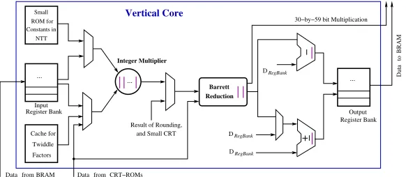
Internal Architecture of the PAU: In Fig. 2 we show the internal architec-ture of the vertical cores that we use inside the horizontal processors in Fig. 1. We follow the pipelined RLWE encryption architecture presented in Fig. 2 of [35] and design our cores to support additional computations required in the YASHE scheme. We design the cores in a more generic way such that a single core can perform computations with respect to several moduli.
The input register bank in Fig. 2 contains registers to store data from the BRAMs and data from the CRTUs. In addition, the register bank also contains shift registers to delay the input coefficients in a pipeline during a NTT compu-tation (see [35] for more details). The register bank has several ports to provide data to several other components present in the core. We use the common name
Dregbank to represent all data-outputs from the register bank. The small ROM
block in Fig. 2 contains the twiddle factors and the value of N−1 to support
/* This module computes butterfly operations */ 1 modulebutterfly-core(inputc; outputm, address1, address2, s1,c, s2,c, s3,c, s4,c)
2 begin
3 (Itwiddle,offset)←(N/2,1)
4 form= 0tologN−1do
5 ωm←2m-th primitiveroot(1)
6 Nbutterfly←0 /* Counts the number of butterfly operation in am-loop */
7 ω←ωm,c /* Initialization to a power of ωm for a core-indexc */
8 forbase= 0to base<offsetdo
9 increment←0
10 whilebase+offset+increment< N
2v do
11 (address1, address2)←(base+increment,base+offset+increment)
12 (t1, u1)←M EM ORYc[address1] /* Read fromc-th group of RAMs */
13 (t2, u2)←M EM ORYc[address2]
14 ifm <logN−1then
15 (t1, t2)←(ω·t1, ω·t2)
16 (s1,c, s2,c, s3,c, s4,c)←(u1+t1, u1−t1, u2+t2, u2−t2)
17 Nbutterfly←Nbutterfly+ 2
18 increment=increment+ 2·offset
19 ifNbutterfly≡Itwiddlethen ω←ω·ωv/m2
20 else
21 t1←ω·t1;ω←ω·ωmv/2
22 t2←ω·t2;ω←ω·ωmv/2
23 (s1,c, s2,c, s3,c, s4,c)←(u1+t1, u1−t1, u2+t2, u2−t2)
24 Nbutterfly←Nbutterfly+ 2
25 increment=increment+ 2·offset
26 Itwiddle←Itwiddle/2
27 ifoffset< v/2then offset←2·offset
/* This module writes the coefficients computed by two butterfly-cores */
28 modulememory-write(inputc, m, address1, address2, s1,0, . . . s4,v−1)
29 begin
30 if2m< v
2 thengap←2
m
31 elsegap← v2 /* This represents the index gap between the two cores */
32 ifc < v/2then
33 M EM ORYc[address1]←(s2,c, s1,c)
34 M EM ORYc[address2]←(s2,c+gap, s1,c+gap)
35 else
36 M EM ORYc[address1]←(s4,c, s3,c) 37 M EM ORYc[address2]←(s4,c+gap, s3,c+gap)
/* This is the top module that executesbutterfly-core in parallel */
38 moduleParallel-NTT() 39 begin
40 butterfly-corebc0(0,m, address1, address2, s1,0, s2,0, s3,0, s4,0)
41 memory-writemw0(0,m, address1, address2, s1,0, . . . s4,v−1)
42 . . .
43 butterfly-corebcv−1(v−1, m, address1, address2, s1,v−1, s2,v−1, s3,v−1, s4,v−1)
44 memory-writemwv−1(v−1, m, address1, address2, s1,0, . . . s4,v−1) Algorithm 2: Routing Efficient Parallel NTT usingvcores
ROM block, there are actuallydL
hesuch ROM blocks, since a core is shared by dL
heprimes. The integer multiplier (shown as a circle in Fig. 2) is a 30×30-bit
two reasons. The first reason is that the primes used in this implementation are not of pseudo-Mersenne type which support fast modular reduction technique [26]. The second reason is that the cores are shared by several prime moduli, and hence, a generic reduction circuit is more preferable than several dedicated reduction circuits. The Barrett reduction circuit is bit parallel to process the outputs from the bit-parallel multiplier in a flow. The reduction consists of three 31×31-bit multipliers and additional adders and subtractors. The multipliers are implemented by combining two DSP multipliers with additional LUTs. Thus in total, the Barrett reduction block consumes six DSP multipliers. Beside per-forming the modular reduction operations, the multipliers present in the Barrett reduction circuit can be reused to perform 30×59-bit multiplications during the CRT computations. The adder/subtracter and the subtracter circuits after the Barrett reduction block in Fig. 2 are used to compute the butterfly operations during a NTT computation and to perform coefficient-wise additions and sub-tractions of polynomials. Finally, the results of a computation are stored in the output register bank and then the registers are written back in the memory. To achieve high operating frequency, we follow the pipelining technique from [35] and put pipeline registers in the data paths of the computation circuits. In Fig. 2, the pipeline registers are shown as magenta colored lines.
4.2 CRT Unit
We accelerate polynomial arithmetic by representing the polynomials of Rq as smaller residue polynomials moduliqj,j∈[0, l−1]. However, this representation also has the following overhead:
– The multiplication of the input polynomials c1 and c2 in YASHE.Mult is
performed in the larger ringRQ(see Section 2.2). Sincec1andc2are inRq,
we need to first lift the polynomials fromRq to RQ. This lifting operation essentially computes the residue polynomials moduliqj,j ∈[l, L−1] from the residue polynomials moduli qi, i ∈ [0, l−1] by applying the CRT. We call this operation thesmall-CRT.
..
.
DRegBank DRegBank
..
. DRegBank ... Data
to
BRAM
Data from BRAM Datafrom CRT−ROMs Twiddle
Factors
Reduction Vertical Core
Integer Multiplier
Result of Rounding, and Small CRT
Barrett
Register Bank Output 30−by−59 bit Multiplication Small
ROM for
NTT Constants in
Input Register Bank
Cache for
– After the multiplication ofc1andc2, the result is a set of residue polynomials
moduliqj,j ∈[0, L−1]. The scaling operation inYASHE.Mult requires the
coefficients of the result in the form of moduloQ. Hence, we apply the CRT to get back the coefficients moduloQ from the small residue polynomials moduliqj,j∈[0, L−1]. We call this operation thelarge-CRT.
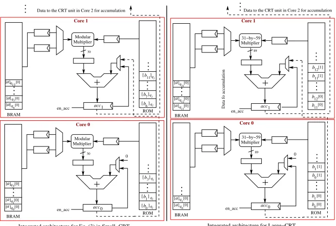
Architecture for the Large-CRT Unit: We compute simultaneous solution with respect to the large modulusQfrom the residues [q]qi fori∈[0, L−1].
[a]Q= X[a]qi·( Q qi
)·[(Q
qi
)−1]qi
Q=
X
[a]qi·bi
Q (1)
Our large-CRT architecture is shown in the right half of Fig. 3. The constant valuesbiare stored in a ROM and then multiplied word-serially with the
coeffi-cients from the BRAMs. We set the word size of the ROMs to 59 bits in order to reuse the 31×59-bit multipliers of the Barrett reduction circuits (Fig. 2) for the 30-by-59 bit multiplications. The computation is distributed among the vertical cores of a processor. In our HE-coprocessor, there are 16 vertical cores in a processor. These cores are divided into twoCRT groups: Core-0 to Core-7 form the first group, whereas Core-8 to Core-15 form the second group. Each group computes one large-CRT in parallel. Since there are 84biconstants (Equa-tion 1), each core in a group computes multiplica(Equa-tions with a maximum of 11
bi constants in parallel and in pipeline. The results of the multiplications are accumulated in the accumulation registers. The partially accumulated results from the cores are added together as follows: the registeracc0is added withacc1
and the result is stored in acc1. Then acc1 is added with acc2 and finallyacc2
is added with acc3. In parallel, acc7 down toacc4 are added together and the
result is stored inacc4. Finally acc4is added with acc3 and the result is stored
in acc3. This final result is then stored in a small distributed RAM (not shown
in the figure) which is read by the DRU. Similar computations are performed in the group consisting of Core-8 to Core-15.
Architecture for the Small-CRT Unit: During a small-CRT computation we first compute the sum of products using the following equation fori∈[0, l−1].
a=X[a]qi·( q qi
)·[(q
qi
)−1]qi = X
[a]qi·bi (2)
This computation is similar to the sum calculation in the large-CRT, but the number of operands is less (maximum of 6 per core) and the size ofbiare small.
We use a similar computation strategy as described in the large-CRT unit. After the computation of a we compute [a0]qj for j ∈ [l, L−1] using the following
equation.
[a0]qj = X
[a]qi·[bi]qj
qj (3)
Here [bi]qj are 30-bit integers. The architecture for this computation is shown
acc0 acc1 acc0 b acc1 q0 q 1 a
[]q11[0]
a
[]q12[0]
a
[ q
21[0]
]
b0[0]
1
b[0]
b0[1]
1
b[1]
b12[1]
11
b[1]
ROM [a]q5
0 0 b b0 b b5 30 Multiplier Modular BRAM 30 en_acc en_acc
Integrated architecture for Large−CRT
en_acc b 11[0] 12[0] 89 Multiplier BRAM en_acc
Data fo accumulation
Data to the CRT unit in Core 2 for accumulation
a [ ] [a]
Multiplier Modular
BRAM
a]
[
[a]
[0]
q0
q1[0]
q
q[0]
[ ]a
Multiplier
89
[0]
[a] [0]
BRAM
31−by−59 31−by−59
Integrated architecture for Eq. (3) in Small−CRT [0] ] ROM [ [ ] b [b 6 7 ] 11 ] ROM Data to the CRT unit in Core 2 for accumulation
Core 0
Core 1 Core 1
Core 0 6
7
[a]q11
[0] [0] [ [ ] 1q ] [ q q ql l l ql q l l
Fig. 3.Architecture for the Small and Large CRT. The computation blocks are aligned along a horizontal processor. Exchange of data between the cores occur during a Large-CRT computation.
multiplier that is present inside the vertical cores present of a processor in our HE-coprocessor. The cores in the two CRT groups compute in parallel and in pipeline. Each core computes a maximum of 6 modular multiplications (since there are 43qj modulus and 8 cores in a CRT group). The accumulation of the partially computed results from one core to the next core is performed in the same way as described in the large-CRT unit. Finally, we compute the residues [a]qj forj∈[l, L−1] using the following equation:
[a]qj =
[a0]qj −[ba/qc]qj ·[q]qj
qj (4)
This computation involves a division of a by q which is performed using the division unit in parallel to the computation of (3). The division architecture is described in the next section.
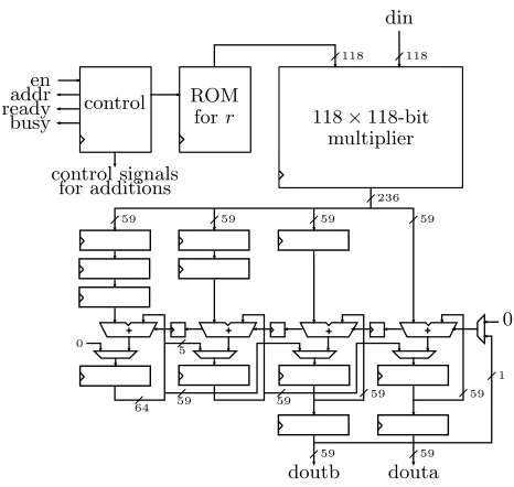
4.3 Division and Rounding Unit
en
118×118-bit
236
multiplier
59 59
59 59
59 59
ROM forr
118 118
control signals
din
doutb douta
for additions
5
59
1
0
59 59 59
64
control addr
ready busy
0
Fig. 4.The Division and Rounding Unit (DRU)
size < q2
i. The word size of the DRU was selected to be 118 bits (2×59) as a
compromise between area and latency.
To round a division of two k-bit integers correctly to k-bits, the quotient must be computed correctly to 2k+ 1 bits [27, Theorem 5.2]. In our case, the computation ofbtc/qerequires a division of ak1-bit dividend by ak2-bit divisor.
The precision that we will need in this case to guarantee correct rounding, based on the above, is k1+k2+ 1 bits. The divisor q is a 1228-bit constant integer
and the dividendc is an at most 2492-bit integer1, which gives a bound of 3721 bits. Hence, the reciprocalris computed up to a precision of 32 118-bit words, of which 22 words are nonzero.
Figure 4 shows the architecture of the DRU. The multiplication r×c is computed by using a 118×118-bit multiplier that computes 222= 484 partial multiplications. This multiplier performs a 118-bit Karatsuba multiplication by using three 59×59-bit multipliers generated with the Xilinx IP Core tool (which supports only up to 64-bit multipliers). The 59-bit multipliers each require 16 DSP blocks giving the total number of 48 DSP blocks. In order to achieve a high clock frequency, the 118-bit multiplier utilizes a 23-stage pipeline, of which 18 stages are in the 59-bit multipliers (the optimal number according to the tool). The partial products from the 118-bit multiplier are accumulated into a 241-bit (2×118 + 5) register using the Comba algorithm [12]. These additions are computed in a 4-stage pipeline with three 59-bit adders and one 64-bit adder,
1 The dividend c is a sum of 216 integers, each in [0,(q−1)2] (2455-bit integers).
Table 1.The area results on Xilinx Virtex-7 XCV1140TFLG1930-2 FPGA
Resource Used Avail. Percentage
Slice Registers 323,120 1,424,000 22.6 %
Slice LUTs 377,368 712,000 53 %
BlockRAM 640 BRAM36, 144 BRAM18 1,880 37.8 %
DSP48 1,792 3,360 53 %
which are all implemented with LUTs. Whenever all partial products of an out-put word have been comout-puted, the register is shifted to the right by 118 bits and the overflowing bits are given at the output of the DRU. Once the compu-tation proceeds to the first word after the fractional point, then the msb of the fractional part is added to the register in order to perform the rounding. The DRU has a constant latency of 687 clock cycles per coefficient.
The DRU is reused for computingbc/qcduring the small-CRT. The compu-tation proceeds analogously to the above. The differences are that the reciprocal is nowr= 1/qand it needs to be computed only to a precision of 2493 bits (12 nonzero words) because c can be only 36 bits longer thanq. The computation has a latency of 246 clock cycles per division.
5
Results
The HE-coprocessor proposed in Sect. 4 was described using mixed Verilog and VHDL. We compiled the processor for Xilinx Virtex-7 XC7V1140T-2, the largest device of the Virtex-7 FPGA family, by using the Xilinx ISE 13.4 Design Suite. We set the optimization goal in the ISE tool tospeed. All results reported in the section have been obtained after place-and-route analysis.
The HE-coprocessor hash= 8 horizontal processors, each havingv= 16 par-allel vertical cores for performing polynomial arithmetic, two small-CRT com-putation groups, two large-CRT comcom-putation groups and two DRUs. The area counts of our HE-coprocessor are shown in Table 1. As seen from the table, our HE-coprocessor consumes nearly 50% of the computational elements (LUTs and DSP multipliers) available in the FPGA. To know the maximum number of processors that we can implement in a single FPGA, we performed a de-sign exploration using the Xilinx PlanAhead tool. This tool allows the dede-signer to manually place different components in the FPGA. The Virtex-7 XCV1140 FPGA consists of four super large logic regions (SLRs). From the design explo-ration we have found that we can put two processors in one SLR. If we put three processors in one SLR (occupies around 70% of the SLR-area), then the Xilinx tool reports congestion of routing channels and the place-and-route analysis fails. From this design exploration we conclude that we can implement two processors per SLR, and hence eight processors in one Virtex-7 XCV1140 FPGA.
Table 2.Latencies and timings at 143 MHz after place-and-route
Operation Clocks Time Rel. time†
NTT 47,795 0.334 ms 0.163µs
INTT 51,909 0.363 ms 0.177µs
Poly-add/sub/mult 4,096 0.029 ms 0.014µs
Small-CRT 821,248 5.743 ms 2.804µs
Large-CRT 2,752,512 19.248 ms 9.398µs
Divide-and-round 2,813,952 19.678 ms 9.559µs
YASHE.Add? 24,576 0.172 ms 0.083µs
YASHE.Mult? 17,399,987 121.678 ms 59.413µs
SIMON-32/64? 8,908,793,344 62.299 s 30.419 ms SIMON-64/128? 24,499,181,696 171.323 s 83.653 ms †Time per slot in SIMD operations (in total 2048 slots)
?Excluding interfacing with the computer and the external memory
place-and-route analysis. NTT and INTT computations are performed on poly-nomials of N = 216 coefficients. To save memory requirement, we compute the
twiddle factors on the fly at the cost of N integer multiplications. One NTT computation using v = 16 cores requires (N+N2 log2(N))/16, i.e. 36,864 mul-tiplications. However the computation of the twiddle factors in the pipelined data path of the PAU (Fig. 2) has data dependencies and thus causes bubbles in the pipeline. Following [35], we use a small register-file that stores four con-secutive twiddle factors, and reduce the cycles spent in the pipeline bubbles to around 10,000. In the case of an INTT computation, the additional cycles are spent during scaling operation byN−1. Cycle count per coefficient for the small-CRT is 401. Since there are two small-CRT groups per processor and there are total eight processors in our HE-coprocessor, for a polynomial with 215 = 32,768 coefficient, the total cost of small-CRT is 821,248 cycles. Similarly, the costs of large-CRT and the division-and-rounding are 672 and 687 cycles per coeffi-cient respectively. However, the cycles spent for the large-CRT operations are not a part of the actual cost, as the large-CRT operation runs in parallel with the division-and-rounding operations during a homomorphic multiplication. The division-and-rounding operations are computed 216 times using 16 DRUs (two
from each horizontal processor) at the cost of 2,813,952 cycles.
Table 2 includes estimates for the latencies ofYASHE.AddandYASHE.Multas well as the evaluations of SIMON-32/64 and SIMON-64/128. TheYASHE.Mult
computes small-CRT, polynomial multiplication, scaling andYASHE.KeySwitch
operations. The cycle count forYASHE.Mult is derived as follows. First the in-put polynomials c1 and c2 are lifted from Rq to RQ using small-CRTs of the
by t/q is performed to compute c0. The YASHE.KeySwitch operation, which is
hWordDecompw,q(c0), evki, uses NTT of the fixedevk (22 polynomials) and de-composes c0 into 22 polynomials. First 22 NTTs and then 22 coefficient-wise multiplications, followed by 21 coefficient-wise additions are performed. Finally one INTT is computed and the result is reduced using Barrett reduction (2 NTTs, 2 INTTs, 2 coefficient-wise multiplications, and 1 coefficient-wise sub-traction). All these computations are performed in six batches. Estimates for SIMON consider onlyYASHE.Mult, which dominate the costs of function evalu-ations. SIMON-32/64 and SIMON-64/128 require 512 (32 rounds with 16 ANDs) and 1,408 (44 rounds with 32 ANDs) YASHE.Mult, respectively. In addition to the latencies and timings for a single execution of the operations, we also provide the relative timings which represent the timings per slot (in total 2048 slots).
Lepoint and Naehrig [29] presented C++ implementations for homomorphic evaluations of SIMON-32/64 and SIMON 64/128 with YASHE running on a 4-core Intel Core i7-2600 at 3.4 GHz. They reported computation times of 1029 s (17.2 min) and 4193 s (69.9 min) for SIMON-32/64 and SIMON-64/128 using all 4 cores, respectively. The implementations included 1800 and 2048 slots and, hence, the relative times per slot were 0.57 s and 2.04 s, respectively. With one core, they achieved 16500 s (275 min) for SIMON-64/128. The homomorphic evaluation of SIMON-64/128 on our FPGA implementation takes 171.3 s (2.85 min) and it also allows 2048 slots giving a relative time of only 83.6 ms per slot. Hence, our single FPGA implementation offers a speedup of up to 24.5 (or 96.32) times compared to the 4-core (or 1-core) software implementation.
6
Conclusions and Future Work
We showed that modern high-end FPGAs (such as Virtex-7) have sufficient logic, hardwired multipliers, and internal memory resources for efficient computation of primitives required for evaluating functions on FHE encrypted data. Despite this, memory requirements and the speed of memory access is critical. Only ci-phertexts that are currently being processed fit into the internal memory of the FPGA and other ciphertexts must be stored in external memory. Interface with the external memory may become a bottleneck unless it is done with special care. Sufficiently fast memory access can be achieved by using high bandwidth mem-ory and/or parallel memmem-ory chips. Many FPGAs include dedicated transceivers for fast interfacing that could be used for fast data access in FHE computa-tions. Moreover, most of the memory access can be performed in parallel with computation using a ping-pong scheme of two sets of BRAMs in the FPGA. The FPGA and the master-computer operate on these two sets alternatively between two consecutive instructions: when the FPGA operates on the first set, the master-computer operates on the second, and vice versa.
homomorphic evaluations independently of each other. This approach improves throughput, but the latency of an individual evaluation remains the same. The second approach is to divide independent homomorphic operations inside a single homomorphic evaluation to parallel FPGAs. Thanks to the numerous indepen-dent computations included, e.g., in homomorphic evaluations of block ciphers, this approach is likely to improve both throughput and latency. While this is conceptually a simple approach, it may still face difficulties because data needs to be transferred between multiple FPGAs. The third option is to divide dif-ferent parts of a homomorphic multiplication to difdif-ferent FPGAs and perform them in a pipelined fashion in order to increase throughput. The fourth option is to mix the other three options and it may lead to good tradeoffs that avoid the disadvantages of the other options. The techniques represented in this paper can be extrapolated to support these options.
The SIMD approach achieves high throughput, but it has been argued that low latency can be more important in practice [29]. The leading software imple-mentation [29] requires as much as 200 s for a single slot evaluation of SIMON-32/64 with YASHE. Our FPGA-based implementation achieves smaller latencies even for SIMON-64/128 with an implementation that allows 2048 slots. Reduc-ing the number of slots to one would allow more efficient parameters (see Sect. 2). We plan to investigate such schemes in the future.
We evaluated the performance of our architecture for YASHE by providing performance values for SIMON in order to provide straightforward comparisons to the leading software implementation from [29]. However, SIMON is not neces-sarily an optimal cipher for FHE purposes. For instance, the low-latency Prince cipher [5] may lead to better performance [19]. FHE-friendly symmetric encryp-tion that is designed to minimize the multiplicative size and depth can offer significant improvements over SIMON (and Prince) [2, 9]. Our architecture is able to evaluate arbitrary functions (up to a certain multiplicative depth) and, hence, these options will be studied in the future. Performance can be further in-creased by tuning the parameters of the architecture for these specific functions. Such changes can be easily done because our architecture is highly flexible.
parallelism on various levels and degrees of parallelism in different parts of the architecture should be fine-tuned to achieve optimal resource utilization and performance. Our source code is highly flexible and significant parts of it were generated with scripts. This allows us to perform parameter space explorations that will enable us to find more optimal parameters for the architecture.
Acknowlegments
S. Sinha Roy was supported by Erasmus Mundus PhD Scholarship, K. J¨arvinen was funded by FWO Pegasus Marie Curie Fellowship and V. Dimitrov was sup-ported by NSERC. This work was supsup-ported by the Research Council KU Leu-ven: TENSE (GOA/11/007), by iMinds, by the Flemish Government, FWO G.0550.12N, G.00130.13N and FWO G.0876.14N, by the Hercules Foundation AKUL/11/19, by the European Commission through the ICT programme un-der contract FP7-ICT-2013-10-SEP-210076296 PRACTICE, and by H2020-ICT-644209 HEAT. We thank Nele Mentens, Jochen Vandorpe, and Jo Vliegen for their help with the Xilinx PlanAhead tool and we thank Ho Truong Phu Truan from NTU, Singapore.
References
1. Xilinx 7 Series FPGAs Overview, DS180 (v1.16.1) December 17, 2014, http://www. xilinx.com/support/documentation/data sheets/ds180 7Series Overview.pdf 2. Albrecht, M., Rechberger, C., Schneider, T., Tiessen, T., Zohner, M.: Ciphers for
MPC and FHE. In: Advances in Cryptology – EUROCRYPT 2015. Lecture Notes in Computer Science, vol. 9056, pp. 430–454. Springer Berlin Heidelberg (2015) 3. Aysu, A., Patterson, C., Schaumont, P.: Low-cost and Area-efficient FPGA
Imple-mentations of Lattice-based Cryptography. In: HOST. pp. 81–86. IEEE (2013) 4. Beaulieu, R., Shors, D., Smith, J., Treatman-Clark, S., Weeks, B., Wingers, L.:
The SIMON and SPECK families of lightweight block ciphers. Cryptology ePrint Archive, Report 2013/404 (2013), http://eprint.iacr.org/
5. Borghoff, J., Canteaut, A., G¨uneysu, T., Kavun, E.B., Knezevic, M., Knudsen, L.R., Leander, G., Nikov, V., Paar, C., Rechberger, C., Rombouts, P., Thomsen, S.S., Yal¸cın, T.: PRINCE — a low-latency block cipher for pervasive computing ap-plications. In: Wang, X., Sako, K. (eds.) Advances in Cryptology — ASIACRYPT 2012. Lecture Notes in Computer Science, vol. 7658, pp. 208–225. Springer (2012) 6. Bos, J.W., Lauter, K., Loftus, J., Naehrig, M.: Improved security for a ring-based fully homomorphic encryption scheme. In: Stam, M. (ed.) Proceedings of the 14th IMA International Conference on Cryptography and Coding (IMACC 2013). Lec-ture Notes in Computer Science, vol. 8308, pp. 45–64. Springer (2013)
7. Brakerski, Z.: Fully homomorphic encryption without modulus switching from clas-sical GapSVP. In: Safavi-Naini, R., Canetti, R. (eds.) Advances in Cryptology — CRYPTO 2012. Lecture Notes in Computer Science, vol. 7417, pp. 868–886. Springer (2012)
9. Canteaut, A., Carpov, S., Fontaine, C., Lepoint, T., Naya-Plasencia, M., Pail-lier, P., Sirdey, R.: How to compress homomorphic ciphertexts. Cryptology ePrint Archive, Report 2015/113 (2015), http://eprint.iacr.org/
10. Cao, X., Moore, C., O’Neill, M., Hanley, N., O’Sullivan, E.: High-speed fully homomorphic encryption over the integers. In: B¨ohme, R., Brenner, M., Moore, T., Smith, M. (eds.) Financial Cryptography and Data Security Workshops, the 2nd Workshop on Applied Homomorphic Cryptography and Encrypted Comput-ing (WAHC 2014). Lecture Notes in Computer Science, vol. 8438, pp. 169–180. Springer (2014)
11. de Clercq, R., Sinha Roy, S., Vercauteren, F., Verbauwhede, I.: Efficient soft-ware implementation of ring-LWE encryption. Cryptology ePrint Archive, Report 2014/725 (2014), http://eprint.iacr.org/
12. Comba, P.G.: Exponentiation cryptosystems on the IBM PC. IBM Systems Journal 29(4), 526–538 (1990)
13. Cormen, T., Leiserson, C., Rivest, R.: Introduction To Algorithms. http://staff. ustc.edu.cn/∼csli/graduate/algorithms/book6/toc.htm
14. Coron, J.S., Lepoint, T., Tibouchi, M.: Scale-invariant fully homomorphic encryp-tion over the integers. In: Krawczyk, H. (ed.) Public-Key Cryptography — PKC 2014, Lecture Notes in Computer Science, vol. 8383, pp. 311–328. Springer (2014) 15. Cousins, D.B., Rohloff, K., Peikert, C., Schantz, R.: SIPHER: Scalable implemen-tation of primitives for homomorphic encryption — FPGA implemenimplemen-tation using Simulink. In: Proceedings of the 15th Annual Workshop on High Performance Em-bedded Computing (HPEC 2011) (2011)
16. Cousins, D.B., Rohloff, K., Peikert, C., Schantz, R.: An update on SIPHER (scal-able implementation of primitives for homomorphic encryption) — FPGA imple-mentation using Simulink. In: Proceedings of the 2012 IEEE High Performance Extreme Computing Conference (HPEC ’12). pp. 1–5 (2012)
17. van Dijk, M., Gentry, C., Halevi, S., Vaikuntanathan, V.: Fully homomorphic en-cryption over the integers. In: Gilbert, H. (ed.) Advances in Cryptology — EURO-CRYPT 2010. Lecture Notes in Computer Science, vol. 6110, pp. 24–43. Springer (2010)
18. Dor¨oz, Y., ¨Ozt¨urk, E., Sunar, B.: Evaluating the hardware performance of a million-bit multiplier. In: Proceedings of the 16th Euromicro Conference on Digital System Design (DSD 2013). pp. 955–962 (2013)
19. Dor¨oz, Y., Shahverdi, A., Eisenbarth, T., Sunar, B.: Toward practical homomor-phic evaluation of block ciphers using Prince. In: B¨ohme, R., Brenner, M., Moore, T., Smith, M. (eds.) Financial Cryptography and Data Security Workshops, the 2nd Workshop on Applied Homomorphic Cryptography and Encrypted Comput-ing (WAHC 2014). Lecture Notes in Computer Science, vol. 8438, pp. 208–220. Springer (2014)
20. Fan, J., Vercauteren, F.: Somewhat practical fully homomorphic encryption. Cryp-tology ePrint Archive, Report 2012/144 (2012), http://eprint.iacr.org/
21. von zur Gathen, J., Gerhard, J.: Modern Computer Algebra. Cambridge University Press, New York, NY, USA (1999)
22. Gentry, C.: Fully homomorphic encryption using ideal lattices. In: Proceedings of the 41st ACM Symposium on Theory of Computing (STOC 2009). pp. 169–178 (2009)
24. Gentry, C., Halevi, S., Smart, N.P.: Homomorphic evaluation of the AES circuit. In: Safavi-Naini, R., Canetti, R. (eds.) Advances in Cryptology — CRYPTO 2012, Lecture Notes in Computer Science, vol. 7417, pp. 850–867. Springer (2012) 25. Gentry, C., Sahai, A., Waters, B.: Homomorphic encryption from learning with
errors: Conceptually-simpler, asymptotically-faster, attribute-based. In: Canetti, R., Garay, J.A. (eds.) Advances in Cryptology — CRYPTO 2013, Lecture Notes in Computer Science, vol. 8042, pp. 75–92. Springer (2013)
26. Hankerson, D., Menezes, A.J., Vanstone, S.: Guide to Elliptic Curve Cryptography. Springer-Verlag New York, Inc., Secaucus, NJ, USA (2003)
27. Karp, A.H., Markstein, P.: High-precision division and square root. ACM Trans-actions on Mathematical Software 23(4), 561–589 (1997)
28. Ko¸c, C.K. (ed.): Cryptographic Engineering. Springer (2009)
29. Lepoint, T., Naehrig, M.: A comparison of the homomorphic encryption schemes FV and YASHE. In: Pointcheval, D., Vergnaud, D. (eds.) Progress in Cryptology — AFRICACRYPT 2014. Lecture Notes in Computer Science, vol. 8469, pp. 318– 335. Springer (2014)
30. L´opez-Alt, A., Tromer, E., Vaikuntanathan, V.: On-the-fly multiparty computation on the cloud via multikey fully homomorphic encryption. In: Proceedings of the Forty-fourth Annual ACM Symposium on Theory of Computing. pp. 1219–1234. ACM, New York, NY, USA (2012)
31. Moore, C., Hanley, N., McAllister, J., O’Neill, M., O’Sullivan, E., Cao, X.: Tar-geting FPGA DSP slices for a large integer multiplier for integer based FHE. In: Adams, A., Brenner, M., Smith, M. (eds.) Financial Cryptography and Data Se-curity Workshops, the 1st Workshop on Applied Homomorphic Cryptography and Encrypted Computing (WAHC 2013). Lecture Notes in Computer Science, vol. 7862, pp. 226–237. Springer (2013)
32. Naehrig, M., Lauter, K., Vaikuntanathan, V.: Can homomorphic encryption be practical? In: Proceedings of the 3rd ACM Workshop on Cloud Computing Security Workshop (CCSW 2011). pp. 113–124. ACM (2011)
33. P¨oppelmann, T., G¨uneysu, T.: Towards Practical Lattice-Based Public-Key En-cryption on Reconfigurable Hardware. In: Selected Areas in Cryptography – SAC 2013, pp. 68–85. Lecture Notes in Computer Science, Springer Berlin Heidelberg (2014)
34. Rivest, R.L., Adleman, L., Dertouzos, M.L.: On data banks and privacy homomor-phisms. Foundations of secure computation 4(11), 169–180 (1978)
35. Sinha Roy, S., Vercauteren, F., Mentens, N., Chen, D.D., Verbauwhede, I.: Com-pact ring-lwe cryptoprocessor. In: Batina, L., Robshaw, M. (eds.) Cryptographic Hardware and Embedded Systems CHES 2014, Lecture Notes in Computer Sci-ence, vol. 8731, pp. 371–391. Springer Berlin Heidelberg (2014)
36. Smart, N., Vercauteren, F.: Fully homomorphic encryption with relatively small key and ciphertext sizes. In: Public Key Cryptography PKC 2010, Lecture Notes in Computer Science, vol. 6056, pp. 420–443. Springer Berlin Heidelberg (2010) 37. Smart, N., Vercauteren, F.: Fully homomorphic SIMD operations. Designs, Codes
and Cryptography 71(1), 57–81 (2014)
38. Wang, W., Hu, Y., Chen, L., Huang, X., Sunar, B.: Accelerating fully homomor-phic encryption using GPU. In: IEEE Conference on High Performance Extreme Computing (HPEC 2012). pp. 1–5 (2012)