Design of Sub-circuits of Switched Capacitor
Filter and its Application in ECG Using
0.18µm CMOS Technology
Deeksha Gupta 1, D. S. Ajnar 2, P. K. Jain3P.G. Student (Microelectronics and VLSI Design), Department of E&I, Shri G. S. Institute of Technology and Science
Indore, M.P, India 1
Associate Professor (Microelectronics and VLSI Design), Department of E&I, Shri G. S. Institute of Technology and
Science Indore, M.P, India 2
Associate Professor (Microelectronics and VLSI Design), Department of E&I, Shri G. S. Institute of Technology and
Science Indore, M.P, India3
ABSTRACT: In this paper, design of sub-circuits of switched capacitor filter using 0.18µm CMOS technology. The basic building blocks of switched capacitor filters are sample-and-hold circuit, non-overlapping clock and a gain stage. The fully integrated designs of a low pass filter having cut-off frequency of 150Hz and a high pass filter having cut-off frequency of 0.05Hz using switched capacitor circuits are presented. This combination of a low pass filter and a high pass filter results in a band pass filter which have the bandwidth of 0.05Hz to 150Hz, which is ideal in detecting ECG signals. The filters are made with the help of op-amps whose gain is 47.119 dB.
KEYWORDS: Switched capacitor circuit, High pass filter, Low pass filter, ECG, Filter, Op-amp, Non-overlapping clock
I.INTRODUCTION
Active filters are generally made with the help of resistors, capacitors and op-amps. These filters use the absolute value of resistors and capacitors to set the transfer function. When we move this circuitry to the silicon chip, we find that it is difficult to achieve same functionality in such a reduced area. Secondly, it is wasteful of the silicon area to make resistors and capacitors with the particular values accurately. Designers have overcome this problem by realizing switched capacitor circuits which are simulated as resistances and their time constants are controlled by ratios of capacitor values instead of the actual value of the capacitances. Switched capacitor circuits are built with the help of switches, capacitors and op-amps.
Fig.1. Switched Capacitor Circuit Fig.2. Equivalent Circuit of Fig.1
II.RELATEDWORK
In [1], the author has presented the design of basic circuits of switched capacitor filter on 0.35µm CMOS technology. The designs of sample and hold circuit, non overlapping clock circuit and gain stage are shown. Various analyses of op-amp and other circuits are presented. The gain stage consists of op-amp, switches and capacitors. In [2], authors have presented the design of low pass filter and high pass filter which are ideal for ECG application with 0.35µm CMOS technology. Both the circuits are combined to finally give band pass filter, whose passband is 0.05Hz to 150Hz. ECG signals are basically in the range of ±2mV. Hence the input to these circuits is given in ±2mV range. In [6], design of two-phase non-overlapping clock generators is given for switched capacitor circuits. The circuit takes into account all the non-ideal effects in the clock signal path. It relies on back-to-back inverter structure. Simulation results show that in comparison to Conventional NAND-based phase generator, this circuit contains fewer components and has 5.6 times more accurate phase shift than conventional circuit.
III.PROPOSEDALGORITHM
The circuit used for implementation of switched capacitor filter is shown. Fig.3. shows proposed non overlapping clock circuit. The clock frequency in mixed signal systems is continuously increasing in order to allow processing of signals with higher bandwidth. Such high frequency values pose challenges to the designers. Hence the proposed circuit of Non overlapping clock provides two non overlapping phases with low values of jitter. This circuit relies on back to back inverter structure. This circuit dissipates less power than conventional NAND structure.
will occupy less area and hence will dissipate lesser power. The continuous transfer function of desired low pass filter and high pass filter are
( ) = ( ) = .
Where Hl(s) is low pass filter transfer function, Hh(s) is high pass filter transfer function, is the 3-dB cut-off
frequencies of the respective filters.
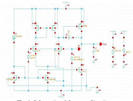
Fig.5. Schematic of Proposed Low Pass Filter
The proposed circuit of low pass filter has lesser components as compared to conventional low pass filter used in ECG application. Hence it will dissipate low power. The circuits of both low pass filter and high pass filters works on power supply in the range ±1.8V.
IV.EXPERIMENTALRESULTS
The simulation results of various blocks of switched capacitor filter is presented. Fig. 7 shows simulation result of non overlapping clock. The gain and phase plot of op-amp is shown in Fig. 8. The gain of op-amp is 47.119dB. This op-amp is further used in implementation of high pass and low pass filter.
Fig.7. Simulation result of Non-Overlapping Clock Fig. 8. Gain and Phase Response of Op-amp
The frequency response of low pass filter is shown in Fig. 9. The cut-off frequency of proposed low pass filter is 149.96Hz. Finally, the frequency response of high pass filter is given in Fig. 10. The cut-off frequency of high pass filter is 51.04 mHz.
The following results are obtained:
Parameter Performance
Gain of Op-Amp 47.119 dB
3dB Frequency of Op-amp 0.7 MHz
Cut-off Frequency of proposed LPF 150 Hz
Cut-off Frequency of HPF 0.05Hz
V.CONCLUSION
In this paper, I have designed sub circuits of switched capacitor filter, high pass filter and low pass filter using switched capacitor circuits and analyzed the waveforms of these circuits. High pass filter having cut-off frequency of around 0.05Hz and low pass filter having cut-off frequency of 150Hz is implemented. The switched capacitor circuits are used to replace resistors. All these blocks are successfully simulated. Further, the circuitry could also be designed on lower CMOS technology for better results and reduced circuitry. The application of the above circuit can further be extended to analog-to-digital converters, digital-to-analog converters and various filters used in applications such as EEG (electroencephalograph), EOG (electrooculogram) and EMG (electromyograph). These applications can be obtained by slight variations of input voltage and frequency range of the above circuit.
REFERENCES
1. Gupta, M, ‘Design Switched Capacitor Filter Sub Circuits Using 0.35u Micron AMS Technology’, International Conference on
Mechanical and Electronics Engineering (ICMEE), Vol.1, pp. V1-6-V1-9, 1-3 Aug. 2010.
2. Chih-Lung Hsiao, Hung-Che Wei, Ren-Bin Huang, Kuang-Ying Tan, ‘A Fully Integrated Switched-Capacitor Filter Design for ECG Application’, IEEE 2nd Global Conference on Consumer Electronics(GCCE), pp. 247-248, 2013
3. P. E. Allen and D. R Hollberg, CMOS Analog Circuit Design, Oxford University Press, 2nd edition, 2002
4. B. Razavi, Design of Analog CMOS Integrated Circuits, McGraw-Hill, First Edition, 1999
5. R. J. Baker, H. W. Li and D. E. Boyce, CMOS Circuit Design, Layout and Simulation, IEEE 1998
6. Blazej Nowacki, Nuno Paulino, Joao Goes, ‘A Simple 1 GHz Non-Overlapping Two-phase Clock Generators for SC Circuits’, 20th
International Conference “Mixed Design of Integrated Circuits and Systems”, Poland, June 20-22, 2013, pp. 174-178
7. WANG Zhu-ping, ZHONG Shun-an, WANG Xiao-qinq, NIE Dan-dan, “Design of a High-precision Low-pass Switched-capacitor Filter”,
2010 International Conference on Electrical and Control Engineering, pp. 707-709, 2010
8. Pai-Chin Lai, “Bandpass Filter Design for ECG Measurement” Master thesis, Univ. Department of Electronic Engineering, Fu Jen Catholic University, July, 2008
9. Ashis Kumar Mal, Rishi Todani, “Non Overlapping Clock (NOC) Generator for Low Frequency Switched Capacitor Circuits” in the proceedings of the 2011 IEEE Students’ Technology Symposium 14-16 January, 2011, IIT Kharagpur, pp. 226-230
10. Kim Y. Wong, Khalid H. Abed, Shailesh B. Nerurkar, “VLSI Implementation of Switched Capacitor Filter”, Dept. of Electrical and Computer Engineering, University of Dayton, 2005
11. Kenneth W. H. Ng, Vincent S. L., Cheung and Howard Luong, A 3-V 44-MHz switched-capacitor band-pass filter for digital video application IEEE International Symposium on Circuits and Systems, 2002.