ISSN(Online): 2320-9801
ISSN (Print): 2320-9798
I
nternational
J
ournal of
I
nnovative
R
esearch in
C
omputer
and
C
ommunication
E
ngineering
(An ISO 3297: 2007 Certified Organization)
Vol. 4, Issue 8, August 2016
Power Efficient 16-bit Shift Register Using
GDI Based Delayed Pulsed Generator and
Dual Edge Latch In 35nm Technology
Shailendra Yadav1, Deepak Kumar2M.Tech Scholar (VLSI Design & Embedded System), Dept. of ECE, RGPV, VIST, Bhopal, M.P., India1
Assistant Professor, Dept. of ECE, Vidhyapeeth Institute of Science and Technology, Bhopal, M.P., India2
ABSTRACT: Power consumption, delay and area reduction play major role in a sequential circuit design. A noble approach to design a dual edged delayed pulse latch based shift register with reduce area and power is proposed. The Shift register is a basic functional unit in digital circuit and image processing such as digital filers, transceivers and image processing ICs. This paper basically focuses on the implementation of the shift register using compact logic of modified delayed clock pulse generator (by using GDI technique) and sequential array of dual edge pulse latches. A 16 bit shift register is designed using latches and delayed clock generator with Vdd=0.3V and simulation isdone byusing Tanner EDA v16.01 TOOL in 35nm CMOS technology.
KEYWORDS: Dual edge pulse latch, GDI (Gate Diffusion Input), Delayed clock pulse generator, Integrated Circuit (IC), Image processing, Complementary metal oxide semiconductor (CMOS).
I. INTRODUCTION
A shift register is a sequential logic circuit which can shift its data in one or both directions. The simplest shift register simply connects the flip-flops to their respective neighbour with the clock controlling the operation. Several D flip-flops may be grouped together with a common clock signal to form a register. Because each flip-flop can store one bit of information, a register with n D flip-flops can store N bits of information. But in recent flip-flops are replaced with pulsed latches for compacting the layout dimensions because pulse latch is smaller than a flip-flop. By using multiple non overlapping trigger signals generated by delayed clock pulse generator, timing problem between pulse latches can be solved. Shift register are commonly used in many applications such as digital filters, communication transceivers and image processing ICs.
The organization of paper starts with a brief introduction pertaining to the section I. There after section II proposes the steps approaching the shift register. Section III illustrate brief description of the proposed architecture of delayed pulsed generator and latches. Section IV comprises the simulation and result of shift register. Finally significant result are summarized in section V.
II. ARCHITECTURE OF SHIFT REGISTER
ISSN(Online): 2320-9801
ISSN (Print): 2320-9798
I
nternational
J
ournal of
I
nnovative
R
esearch in
C
omputer
and
C
ommunication
E
ngineering
(An ISO 3297: 2007 Certified Organization)
Vol. 4, Issue 8, August 2016
Fig. 1. Block diagram of proposed 16bit Shift Register.
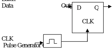
Main components of shift register are Pulsed latch and delayed pulsed clock generator, that are briefly described in this section. Now a days flip-flop is replaced by pulse latch to reduce the power consumption in shift registers. Delay should be introduce to overcome timing problem. It has two inputs data (D), clock (CLK) and a output (Q) as shown in fig. 2.
Latch
Data Output
CLK
Pulse Generator Circuit
Fig. 2. Block diagram of latch with clock pulse.
For generation of non-overlap delayed clock pulse a pulse generator is required. Figure 3 illustrate the basic block diagram of delayed clock pulse generator circuit and also illustrates clock pulse circuit.It uses separate clock pulse circuit, here delay is introduce between the clock pulse circuit to generate delayed clock pulse which does not overlap each other. For bit word length 16 bit shift register requiresdelayed clock pulse generator having five clock pulse circuit with four delay. At the output of clock pulse circuit a buffer is used to produce strong output signalsCP1, CP2, CP3, CP4, Tas shown in fig. 5.
Delayed Clock Pulse Generator
Latch Latch Latch Latch Latch
CP1
CP2
CP4 CP3
T
T1 T2 T3 T4
D Q
CLK
Latch Latch Latch Latch Latch
Latch Latch Latch Latch Latch
Latch Latch Latch Latch Latch
IN Q1 Q2 Q3 Q4
Q5 Q6 Q7 Q8
Q9 Q11 Q12
Q13 Q14 Q15 Q16
ISSN(Online): 2320-9801
ISSN (Print): 2320-9798
I
nternational
J
ournal of
I
nnovative
R
esearch in
C
omputer
and
C
ommunication
E
ngineering
(An ISO 3297: 2007 Certified Organization)
Vol. 4, Issue 8, August 2016
Clock
Pulse
Circuit
CP1 CP2 CP3 - -CP_N
Delayed Clock Pulse Buffer Buffer Buffer Buffer
Generator - -
- -
- -
CLK
Inverters - -
Fig. 3. Block diagram of delayed clock pulse generator.
III.PROPOSED ARCHITECTURE OF DELAYED PULSED GENERATOR AND LATCHES
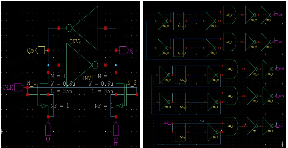
The modified latch uses two cross-coupled inverters in fig. 4 which consist four transistors and update the data with two NMOS transistors N_1 and N_2. It has two differential data inputs D, Db and a clock signal CLK. When clock signal CLK is high both N_1, N_2 turns ON and the input data D, Db is updated. On the contrary when clock signal is low both N_1, N_2 turns OFF. This design uses less amount of transistors than SSASPL.
Fig. 4. Schematic of proposed Latch Fig. 5. Schematic of proposed Delayed clock pulse generator.
Delayed clock pulse generator is implemented similarly shown in fig. 3. In proposed delayed clock pulse generator mod-GDI technique is used for anding clock inputs to generate non-overlapped delayed clock pulses. Fig. 4 and fig. 5 illustrate the schematic of proposed latch and delayed clock pulse generator respectively. Both of these reduce the average power, static power, dynamic power and area.
GDI AND
GATE Clock Pulse
Circuit
Clock Pulse Circuit Delay
ISSN(Online): 2320-9801
ISSN (Print): 2320-9798
I
nternational
J
ournal of
I
nnovative
R
esearch in
C
omputer
and
C
ommunication
E
ngineering
(An ISO 3297: 2007 Certified Organization)
Vol. 4, Issue 8, August 2016
IV.RESULTSANDDISCUSSION
This paper describes the design and implementation of power efficient shift register by using modified delayed clock pulse generator and dual edge latch. Simulation is done using Tanner EDA tool v16.01 in 35 nm technology. The table 1 shows theperformance parameter of Latch, in this table we also compare the number of transistor used in both SSAPL based latch and proposed dual edge latch.
Table 1. Performance parameter comparison of latch.
S. No. Parameters SSASPL Proposed Latch
1. No. of Transistor Total 7 6
Clock 1 2
2. Total power consumption 3.3 0.62
3. Power consumption of data path (uW) 2.57 0.58 4. Power consumption of clock load (uW) 0.73 0.04
Table 2 shows the Performance parameter comparison of Delayed clock pulse generator respectively. It shows the 10 number of transistor is used to implement delayed clock pulse generator circuit on the other hand clock pulse generator requires 14 number of transistor. Hence the proposed delayed clock generator is area efficient. It also consume less power as compare to clock pulse generator.
Table 2. Performance parameter comparison of delayed clock pulse generator.
S. No. Parameters Clock pulse
generator
Proposed delayed clock pulse
generator
1. No. of Transistor 14 10
2. Power consumed by each clock pulse
circuit (uW) 27.6 2.53
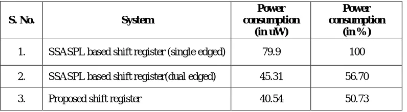
The table 3 show the comparative analysis of proposed shift register with single edge and dual edge SSASPL shift register. Results of power consumption are showing in both microwatt and percentage. Proposed shift register consume 40.54 micro watt which is 50.73 percent of single edged SSASPL based shift register.
Table 3. Performance comparison of 16bit shift register.
S. No. System
Power consumption
(in uW)
Power consumption
(in %)
1. SSASPL based shift register (single edged) 79.9 100
2. SSASPL based shift register(dual edged) 45.31 56.70
ISSN(Online): 2320-9801
ISSN (Print): 2320-9798
I
nternational
J
ournal of
I
nnovative
R
esearch in
C
omputer
and
C
ommunication
E
ngineering
(An ISO 3297: 2007 Certified Organization)
Vol. 4, Issue 8, August 2016
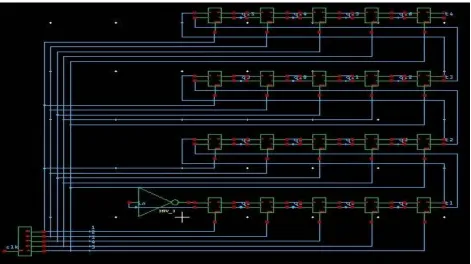
Fig. 6 is showing schematic block diagram of proposed 16 bit shift register. Fig. 7 showing the result of 16 bit shift register, it is a snapshot of log file generated by T-spice.
Fig. 6.Schematic diagram of 16bit proposed shift register.
Fig. 7 showing the result of 16 bit shift register, it is a snapshot of log file generated by T-spice. It shows value of average power consumed which is 4.054153e-005 watts also showing the value and time of maximum and minimum power consumed.
ISSN(Online): 2320-9801
ISSN (Print): 2320-9798
I
nternational
J
ournal of
I
nnovative
R
esearch in
C
omputer
and
C
ommunication
E
ngineering
(An ISO 3297: 2007 Certified Organization)
Vol. 4, Issue 8, August 2016
Fig.8. Waveform of 16bit proposed shift register.
Fig. 8 illustrate the timing diagram of proposed 16 bit shift register here waveform showing transition of input (in) through latches, q13, q14, 15, q16 and t4 is output of latches in forth sub shift register.
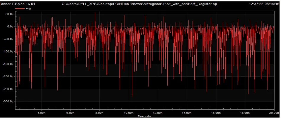
Chart 1.Power consumption graph of proposed 16 bit shift register.
ISSN(Online): 2320-9801
ISSN (Print): 2320-9798
I
nternational
J
ournal of
I
nnovative
R
esearch in
C
omputer
and
C
ommunication
E
ngineering
(An ISO 3297: 2007 Certified Organization)
Vol. 4, Issue 8, August 2016
Chart 2 is showing the comparison of power consumption by proposed 16 bit shift register with SSAPL based shift register in percentage ( % ) and micro watt ( uW ). First two bar indicating power consumed by SSAPL single edge based shift register, the second two bars indicating the power consumption of SSASPL Dual edged and the last two shows the power consumed by the proposed shift register which is less as compare to other two.
Chart2. Comparison of power consumption by proposed 16 bit shift register with SSAPL based shift register.
V. CONCLUSION AND FUTURE WORK
In this paper we have proposed power efficient modified shift register using modified delayed clock pulse generator and duel edge latch. Simulation is done using Tanner EDA v16.01 Tool in 35nm technology. Since our objective was low power consumption in shift register and power consumption is found to be 40.54uW it is 50.73% of SSASPL based shift register (single edged), hence we achieved our objective. In this paper we have design shift register without using MTCMOS or adiabatic technique.Design a shift register using these techniques can lead to enhance overall performance by reducing leakage current.
REFERENCES
1. Byung, Do Yang, ‘Low-power and Area-efficient Shift Register using Pulsed latches’, IEEE Transactions on circuits and systems-I: Regular papers, Vol. 62, No. 6, June 2015.
2. P. Reyes, P. Reviriego, J. A. Maestro, and O. Ruano, ‘New protection techniques against SEUs for moving average filters in a radiation environment’, IEEE Trans. Nucl. Sci., vol. 54, no. 4, pp. 957 –964, Aug. 2007.
3. M. Hatamianetal., ‘Design considerations for gigabit ethernet 1000 base-T twisted pair transceivers’, Proc. IEEE Custom Integr. Circuits Conf., pp. 335–342, 1998.
4. H. Yamasaki and T. Shibata, ‘A real-time image-feature-extraction and vector-generation vlsi employing arrayed-shift-register architecture’, IEEEJ. Solid-State Circuits, vol.42, no.9, pp. 2046 –2053, Sep. 2007.
5. H. S. Kim, J. H. Yang, S. H. Park, S. T. Ryu, and G. H. Cho, ‘A 10-bit column-driver IC with parasitic-insensitive iterative charge-sharing based capacitor-string interpolation for mobile active-matrix LCDs’, IEEEJ. Solid-State Circuits, vol. 49, no. 3, pp.766–782, Mar. 2014.
6. S. H. W. Chiangand and S. Kleinfelder, ‘Scaling and design of a16-megapixel CMOS image sensor for electron microscopy’, in Proc. IEEE Nucl. Sci. Symp. Conf. Record (NSS/MIC), pp. 1249–1256 2009.
7. Athira. B, Dr. B. Jai Shankar, ‘Design of low power area efficient pulse latches based Shift Register’, IJSRD, vol-3, issue-09, 2015.
8. M. Poongodi and P Jayabalasubramaniam, ‘Minimization of power and area by using dual edge latch for SAR and Comparator’, IJERST vol-5, issue-1, Feb 2016.
9. PoojaVerma, RachnaManchanda, ‘Review of various GDI techniques for low power digital circuits’, IJETAE vol-4, issue-2, Feb. 2014.
10. PaanshulDobriyal, Karan Sharma, MananSethi andGeetanjali Sharma, ‘A high performance D-flip flop design with low power clocking system using MTCMOS technique’, IJCE vol-1, 2016.
0 10 20 30 40 50 60 70 80 90 100
SSASPL SSASPL Dual Edge Proposed
Power consumption (in %)
ISSN(Online): 2320-9801
ISSN (Print): 2320-9798
I
nternational
J
ournal of
I
nnovative
R
esearch in
C
omputer
and
C
ommunication
E
ngineering
(An ISO 3297: 2007 Certified Organization)
Vol. 4, Issue 8, August 2016
11. S.-H. W. Chiang and S. Kleinfelder, ‘Scaling and design of a 16-megapixel CMOS image sensor for electron microscopy’, in Proc. IEEE Nucl. Sci. Symp. Conf. Record (NSS/MIC), pp.1249–1256, 2009.
12. C. K. Teh, T. Fujita, H. Hara, and M. Hamada, ‘A 77% energy-saving 22-transistor single-phase-clocking D-flip-flop with adaptive-coupling
configuration in 40nm CMOS’, in IEEE Int. Solid-State Circuits Conf. (ISSCC) Dig. Tech. Papers, Feb.2011, pp.338–339.
13. E. Consoli, M. Alioto, G. Palumbo, and J. Rabaey, ‘Conditional push-pull pulsed latch with 726 fJops energy delay product in 65 nm CMOS’, in IEEE Int. Solid-State Circuits Conf. (ISSCC) Dig. Tech. Papers, pp. 482–483 Feb. 2012.
14. B.-S. Kong, S.-S. Kim, and Y.-H. Jun, ‘Conditional-capture flip-flop for statistical power reduction’, IEEE J. Solid-State Circuits, vol. 36, pp. 1263–1271, Aug. 2001.
15. S. Heo, R. Krashinsky, and K. Asanovic, ‘Activity-sensitive flip-flop and latch selection for reduced energy’, IEEE Trans. Very Large Scale Integr.(VLSI) Syst., vol.15, no.9, pp. 1060–1064, Sep. 2007.
16. V. Zyuban and P. Kogge, ‘Application of STD to latch-power estimation’, IEEE Trans. Very Large Scale Integr. (VLSI) Syst., vol.7, no.1, pp.111–115, Jan. 1999.
BIOGRAPHY