ABSTRACT
MORGENSEN, MICHAEL P. Drain Current Modeling and Characterization using MISFETs. (Under the direction of Dr. Leda Lunardi and Dr. Doug Barlage.)
The effects of interface states on metal-insulator-semiconductor field-effect transistor (MIS-FET) drain current have been investigated using the one-dimensional solution of Poisson’s equation commonly used to develop compact models. The U-like distribution of interface state density throughout the bandgap has been utilized when calculating interface state charge den-sity without resorting to the numerous approximations found in the literature. Consequently, the resulting set of charge expressions are able to correctly predict gate voltage stretch-out in the current-voltage domain. A compact model of trap-affected drain current using the charge sheet approximation has been developed and the challenges highlighted. The computational speed needed by the model is a limiting factor and is caused by the unique relationship be-tween inversion charge density and surface potential not found in standard models excluding interface states.
c
Copyright 2011 by Michael P. Morgensen
Drain Current Modeling and Characterization using MISFETs
by
Michael P. Morgensen
A dissertation submitted to the Graduate Faculty of North Carolina State University
in partial fulfillment of the requirements for the Degree of
Doctor of Philosophy
Electrical Engineering
Raleigh, North Carolina 2011
APPROVED BY:
Dr. Griff Bilbro Dr. Mark Johnson
Dr. Doug Barlage
Co-chair of Advisory Committee
BIOGRAPHY
ACKNOWLEDGEMENTS
I would like to thank Dr. Lunardi for agreeing to act as Committee Chair throughout my Ph.D. research. I greatly benefited from your guidance in technical writing and willingness to offer suggestions for challenging problems. I am also thankful for the encouragement and advising given by Dr. Barlage that began when I was an undergraduate and continued through completion of my Ph.D. Thank you for giving me the opportunity to attend graduate school, something I never had any intention of doing full-time. Thank you to Dr. Johnson and to Dr. Bilbro for serving on my advisory committee and for the useful discussions your questions generated.
I would also like to acknowledge the contributions from my past and present colleagues. Dr. Jaehoon Park, you were an excellent addition to our group and thank you for the many conversations regarding semiconductor physics. Merve Ozbek, thank you for your willingness to assist with simulation questions and also for your support on the day of my defense. Dr. Matt Veety, thank you for all the hard work devoted towards fabricating devices. It’s been quite an experience since our undergraduate days, and I enjoyed the many technical discussions over the years.
TABLE OF CONTENTS
List of Tables . . . vi
List of Figures . . . vii
Chapter 1 Introduction . . . 1
1.1 Overview of contents . . . 4
1.1.1 Optimization details . . . 6
1.1.2 Comments on simulated curves . . . 6
Chapter 2 Charges in the metal-oxide-semiconductor system . . . 8
2.1 Semiconductor charge . . . 10
2.2 The surface potential equation . . . 15
2.3 Quantum mechanical effects . . . 18
2.3.1 Modifications for inversion in p-channel MOS devices . . . 23
2.3.2 Summary of useful charge density expressions . . . 24
2.4 Interface trapped charge . . . 25
2.4.1 Trap occupation . . . 26
2.4.2 Interface trapped charge density . . . 28
2.4.3 Approximating trapped charge density . . . 33
2.4.4 ExpandingQ0it . . . 38
Chapter 3 Drain current . . . 42
3.1 Charge Sheet Approximation details . . . 44
3.2 Behavior of trap-affectedQ0i . . . 49
3.3 Effective Mobility . . . 52
3.4 Calculating drain current . . . 54
3.4.1 Effects ofDit on DC drain current . . . 61
3.4.2 Velocity saturation . . . 66
3.4.3 Series resistances . . . 67
3.4.4 Current saturation . . . 71
3.5 Model Summary . . . 74
Chapter 4 Mobility analysis . . . 76
4.1 Discussion of the mobility measurement from C-V . . . 77
4.1.1 Analytical correction for the trap-free case . . . 82
4.1.2 Accounting for interface states . . . 94
4.2 Mobility from drain current . . . 96
4.2.2 Accounting for interface states . . . 105
Chapter 5 Analysis of the insulator-semiconductor interface through drain current 110 5.1 Doping investigation from capacitance-voltage . . . 113
5.1.1 Extracting effective doping from low frequency C-V measurements . . 117
5.2 Drain current basedDit analysis . . . 119
5.2.1 Method 1 . . . 120
5.2.2 Method 2: arbitrarytox . . . 126
5.3 Application of methods to silicon MOSFETs . . . 132
Chapter 6 Characterization of gallium nitride MISFETs . . . 139
6.1 GaN-specific modeling concerns . . . 140
6.2 Analysis of a three-terminal GaN MISFET . . . 144
6.2.1 Supporting theory . . . 144
6.2.2 Measurement results . . . 150
6.3 Measurement of a four-terminal GaN MISFET . . . 157
Chapter 7 Conclusions and suggested work . . . 163
7.1 Suggested work . . . 165
LIST OF TABLES
LIST OF FIGURES
Figure 2.1 Simple MOSFET cross-section (without gate overlap) showing chosen positioning of axes. . . 9 Figure 2.2 Total semiconductor charge density with different values forV, defined
in the paragraph above equation (2.10). . . 14 Figure 2.3 Plots of surface potential versus gate voltage with varying (a) oxide
thickness, (b) doping, (c) imref splitting. VFB=0V for all curves and
V =0 (unless otherwise indicated). . . 17 Figure 2.4 C-V plots for different oxide thickness values (a) 2.5nm, (b) 25nm,
(c) 50nm, showing the discrepancy between the classical and QM ap-proaches. . . 22 Figure 2.5 Filled/empty states and band bending. . . 25 Figure 2.6 Difference in occupation functions where F is the exact steady-state
version andFFDis the simplified quasi Fermi-Dirac version. The exact version indicates thatV can only push the falling edge leftward until around midgap, at which point the simplified version becomes incor-rect. . . 27 Figure 2.7 Effect of bandtail parameterbon interface state charge density. Without
the Dc term Q0it would increase linearly with respect to ψs and then saturate asEc is bent down towardsEF.V =0. . . 31 Figure 2.8 Effect of different densities on interface state charge density forV =0. . 31 Figure 2.9 Effect of different densities on the surface potential equation fortox=
30nm. In (b), solid line: Di=2×10¹², Dc =5×10¹³; dashed line:
Di=1012,Dc=1013; dot-dashed line:Di=5×10¹¹,Dc=1012. . . . 32 Figure 2.10 Quality of MID. Solid line: developed approximation; closed circles:
exact result. Inset shows percent error forV =0.5 since forV =0 the result is exact. The percent error is the same for other values ofV. . . . 34 Figure 2.11 Magnitude of error associated with the summation and σ integration
approach for V = 0. As the ratio Di/Dc is increased the error will decrease. V =0 and T =25C. All of the error is from CON because MID is exact atV =0. . . 36 Figure 2.12 Magnitude of error associated with the summation and σ integration
approach forV =0.5. As the ratio Di/Dc is increased the error will decrease. . . 37 Figure 2.13 Delta in predicted gate-bulk voltage by evaluating SPE attox=30nm.
Figure 2.14 First derivative of Q0it forV =0 (MOS capacitor case). In (b) each solid exponential line is a plot of Di+Dce(ψs+EF−Ec)/b to investigate the common approximationCit/q≈Dit. The x-axis can be thought of asE−Evsimilar to Figure 2.7. . . 40 Figure 3.1 Surface potential swept fromφF to 3φF (an extreme value but chosen
to show the decrease in error). In (a), the largest curve corresponds to the greatest doping and vice-versa. . . 46 Figure 3.2 Percent error of the drift-diffusion charge sheet model forIdsrelative to
the numerically evaluated Pao-Sah expression. The x-axis is different in (b) because of voltage stretchout byDit. . . 48 Figure 3.3 Legend indicates value ofψs0(source-side surface potential). (a)
demon-stration of linearity when traps are absent. (b)-(d) traps cause non-linearity until a large enough gate bias is applied (strong inversion triode region). VDS = 0.5V, tox = 30nm, NA = 1017cm−3. Qi0,L =
Q0i(ψs0,L,VSB,DB). . . 51 Figure 3.4 Effect of field-dependent mobility on channel inversion charge.requals
µe evaluated at the channel midpoint, which clearly produces a conve-nient alternative to integrating µQ0i. The mobility-affected quantities were normalized byµ0=350cm2/Vs; also,K=6(1014)V/s. Gate bias
chosen to operate simulated device in the triode region. . . 54 Figure 3.5 Percent error of expression (3.19) relative to discretely integrated (3.11).
Lines without markers are for VDS =100mV and lines with markers are forVDS =1V. Higher VDS increases error slightly at larger band-bending. Calculated for special case of unityµeWL to demonstrate qual-ity of approximation toR
Q0idψs. . . 58 Figure 3.6 Percent error of expression (3.20) relative to discretely integrated (3.11)
forVDS =100mV. . . 60 Figure 3.7 Effect of increasing Dc with µeWL =1 cm2/V ·s, NA =1017, b=50
meV, Di =5(1011). The x-axis is shifted for each curve by its initial value. VGS for each curve computed by starting and ending at source-side surface potentialsφF and 1.0V. . . 63 Figure 3.8 Effect of increasingbwithµeWL =1 cm2/V·s,NA=1017,Dc=3(1013),
Di=5(1011). The x-axis is shifted for each curve by its initial value.
VGS for each curve computed by starting and ending at source-side sur-face potentialsφF and 1.0V. . . 64 Figure 3.9 Increasing values oftoxreduce oxide capacitance density and strengthen
Figure 3.11 Characteristics of a simulated device withtox=10nm,NA=1017,Di=
0,Dc=1013, b=0.05, µe=µ0=150. VGS from top to bottom: [3.6,
4, 4.6] V. . . 70
Figure 3.12 Characteristics of a simulated device withtox=10nm,NA=1017,Di= 5(1011),Dc=3(1013),b=0.05,µe=µ0=150,VDS=0.1V. . . 70
Figure 3.13 Top curve to bottom: L=100, 10, 1 um. Markers: numerical search; line: analytical expression. NA=1017cm−3, tox=30 nm, µe =µ0= 100. Threshold is near 2.7V. . . 73
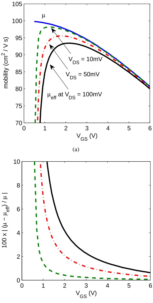
Figure 4.1 Actual mobility and equation (4.5) applied at three different drain bi-ases. All curves tend towards the same limiting value at high gate bias but include some artificial roll-off near threshold (around 0.6V).W =L, NA=1016cm−3,tox=200 ˚A,T =25C, trap-free (same parameters used for any other fictional device results to follow). . . 81
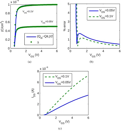
Figure 4.2 Quality of∆for two smallVDS values as function ofVGS. (c) indicates threshold. . . 85
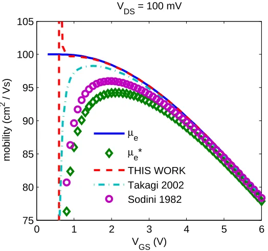
Figure 4.3 Effective mobility atVDS=100 mV. . . 89
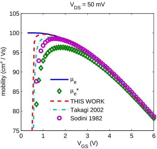
Figure 4.4 Effective mobility atVDS=50 mV. . . 90
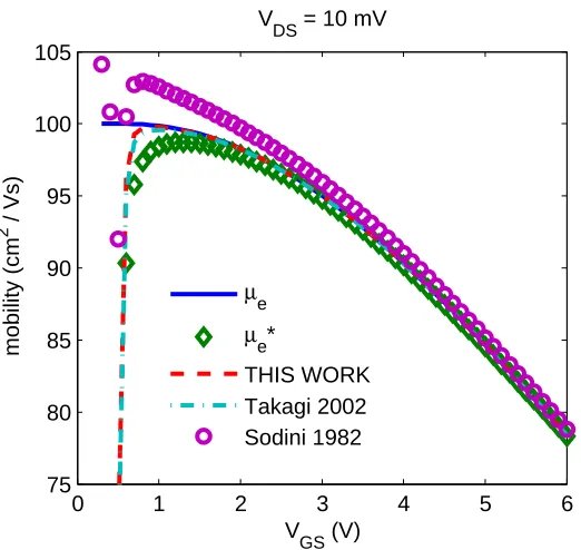
Figure 4.5 Effective mobility atVDS=10 mV. . . 91
Figure 4.6 All data obtained from C.L. Huang (reference in text). The analyti-cal correction works well since doping and oxide thickness were well-known andDit was very low. . . 93
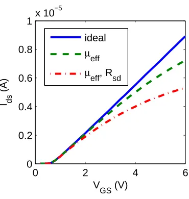
Figure 4.7 Drain current reduced by series resistance and field-dependent mobility. Rsd=5kΩ. . . 98
Figure 4.8 Dotted line indicates the linear fit. (a) estimates µ0 as 102, compared to 100 actual. (b) estimatesθ2as 6.99·(10−3)V−2, compared to 6.94· (10−3)V−2 actual. (c) estimates θ1e as 9.55·(10−2)V−1, compared to 9.67·(10−2)V−1actual. (d) is the fit after direct extraction with equa-tion (4.31). . . 102
Figure 4.9 The digitized data from C.L. Huang is indicated with markers (refer-ence given in text). The slope of (a) is related to µ0 and the slope of (b) is θ1. In (c) the fit using equation (4.21) is compared against the measured data. Because of the noise in (a) atVDS=20mV the low field mobility is overestimated, worsening the result in (c). . . 104
Figure 4.10 Behavior of transconductance and subparts ofQ0ifor a trap-free device. Parameters of the simulated device: tox=200 ˚A, NA=1016cm−3, µ = 100/(1+Ee2/E02),E0=106MV/cm,VFB=−0.5V. . . 107
Figure 4.11 Behavior of transconductance and subparts ofQ0ifor a constantDit. . . 107
Figure 4.13 Behavior of transconductance and subparts ofQ0i for exponentially in-creasingDit. . . 108 Figure 4.14 Behavior of transconductance and subparts ofQ0i for exponentially
in-creasingDit for different value ofb. . . 109 Figure 5.1 Example doping profiles and the resulting bias-dependent effective
dop-ing found from the finite difference method. . . 118 Figure 5.2 EOT is the equivalent oxide thickness relative to SiO2. . . 120
Figure 5.3 Mobility extracted fromIds/√gmin its linear region. A large increase inDit near the minority carrier band edge reduces the apparentµ0. tox= 200 ˚A,Di=0,VDS=10mV. . . 121 Figure 5.4 Validity of result one obtains by assuming trap-free and trap-affected
currents occur at the same source-side surface potential, ψs0. Percent
error in (a). Simulated device with constant µ =100cm2/Vs, Di = 1e12eV−1cm−2, Dc = 2e13eV−1cm−2, b = 0.1eV, NA = 1016cm−3,
tox=200 ˚A. . . 123 Figure 5.5 Method 1 operated on a simulated device. Same parameters as in Figure
5.4. . . 125 Figure 5.6 Inset of (a) is the random sequence of integers scaled to give plus or
minus 1.5% variation. The noise is not apparent on the plot in (a) until calculation of discrete derivative used for quantityM. (b) shows opti-mization outcome at Ion/Ioff =5000 where the “measured” symbols correspond to simulated current generated for (a). . . 131 Figure 5.7 Method 2 and measurement uncertainty. . . 131 Figure 5.8 Measured and fit ratio of transconductance to current for two n-channel
MOSFETs.VDS=100mV. . . 135 Figure 5.9 Measured and fit ratio of transconductance to current for three p-channel
MOSFETs.VDS=100mV. . . 136 Figure 5.10 Combined effective mobility implied by results of Method 2. . . 137 Figure 5.11 Dit distribution implied by Method 2. . . 138 Figure 6.1 Theoretical surface potential curves. SPEMB is SPE with
Maxwell-Boltzmann statistics; SPEFD is SPE with Fermi-Dirac statistics. For Si: Nc =3.2×1019cm−3. For GaN: Nc =2.2×1018cm−3. VT0 is the
long-channel threshold voltage. Due to the strong deviation in ψs at
tox=10nm it is likely that quantum confinement should be considered in a device model. . . 143 Figure 6.2 Equivalent circuit for the small signal response of interface states. Cc
Figure 6.3 Voltage stretchout and frequency dependence related to interface states. Top dotted line is related toCg0(f →0); bottom dotted line isCg0(f → ∞). Solid lines from left to right: 1kHz, 31.6kHz, 1MHz. The title
in each plot gives the interface state density relative to the oxide ca-pacitance density. (b) is an extreme case where greater than 15V of stretchout occurs. . . 149 Figure 6.4 Capacitance and conductance results over a range of frequencies. (c) is
the corrected curve after deembedding oxide capacitance density, and (d) is the rescaled version showing the peak moving downward in fre-quency. The dotted line in (a) indicates the estimated oxide capacitance. 151 Figure 6.5 Representative GaN MISFET that could survive out to very high gate
voltages. From C-V, SiO2thickness is around 70 nm. The fluctuation in
(c) is the result of discrete differentiation, which has “amplified” some minor deviation in (a). The minor deviation in (a) could be attributed to the measurement equipment, poor probe contact to pads, or some small change in the interface properties due to biasing. . . 154 Figure 6.6 Outcome of Method 2 applied to the data in Figure 6.5. In (a) the
markers represent measured data, solid lines are the fit. In (b) both the lines and markers represent the resulting mobility.W =L=64um and
tox≈70nm. . . 155 Figure 6.7 Reconstructed ideal case for device of Figure 6.5 whereDit=0. . . 156 Figure 6.8 Real and imaginary components of the gate small-signal response. 20
frequencies evenly spaced logarithmically from 1kHz (left-most curve) to 1MHz (right-most curve). Series resistances reduce the peak capaci-tance at high frequencies. Representative plot of typical device. . . 159 Figure 6.9 The family of curves are tilted upward by the presence of junction
leak-age. Representative plot of typical device. . . 160 Figure 6.10 Log and linear scale plots of drain current showing how Ion toIo f f is
not much greater than a decade. Representative plot of typical device. . 161 Figure 6.11 One quadrant (repeated in three other quadrants) in a 1 cm x 1 cm
Chapter 1
Introduction
The introduction of alternative insulator and substrate materials for metal insulator semicon-ductor field-effect transistor (MISFET) fabrication has the potential to create non-idealities in the insulator-semiconductor interface properties, an area greatly improved for the silicon metal oxide semiconductor field-effect transistor (MOSFET) over the past five decades [1]. These non-idealities collectively violate the basic assumption on which most electrical MOS-FET models are built, namely that the only source of bias-dependent charge is from the semi-conductor itself. A model that incorporates interface non-idealities could therefore be useful and flexible in gauging improvement in fabricated devices.
substantially depending on the quality of the surface passivation and how effective it is in limiting the trapping process [3]. The interface state density (defined asDit) as a function of energy can be described empirically with a pair of exponentials and is often described as U-like [4]. TheDit distribution has alternatively been modeled using sums of Gaussians [5] that could resemble a U-like distribution depending on the Gaussian parameters.
In a MOSFET the applied gate bias directly controls the charges present underneath the gate electrode. By charge conservation, the sum of all charges below the gate equals the total gate charge. Interface states if present will contribute a charge density that varies with band-bending along with the semiconductor charge density. As gate bias changes, both interface state charge density and semiconductor charge density will respond in balancing the gate charge. Therefore, at a given gate bias the semiconductor charge density varies from the value without interface states. From an electrical measurement point of view this behavior is termed gate voltage stretch-out.
Voltage stretch-out absent in optimized devices is not usually included in models for inte-grated circuit simulation. However, its inclusion would allow for better understanding between measured and simulated electrical data of non-optimized devices and device parameter extrac-tion. In this work the electrical data of interest is MOSFET drain current. Including stretch-out in drain current has been attempted over localized gate bias regions by considering simplifica-tions of the expression forDit. The complexity of exact inclusion lies in the definition of the interface trapped charge expression, written as an integral over the bandgap of density of states with an occupation probability [6]. While the inclusion of interface states is important for cor-rectly describing drain current from weak through strong inversion, the necessary integral for a U-like description is not easily solved or approximated.
over all gate biases. P. Muls used this simplification to develop closed-form approximations for drain current in weak inversion [7]. Extending the result outside weak inversion is feasible but would involve some degree of approximation for the integration of inversion charge density to determine drain current [8, 9]. Unless a U-like distribution is considered, a constant interface state density cannot explain the slow transition between linear region drain current and that in subthreshold. It would be more accurate to consider an energy-dependentDit function for real devices when modeling drain current from subthreshold through strong inversion.
Common approaches that include the distribution over energy for calculating drain current are either simplified or completely numerical. These approaches can be found in the domain of silicon carbide MOSFETs and were deemed necessary in order to gain theoretical under-standing of measured device behavior since SiC MOSFETs have been found to suffer from very high interface state density [10]. The most common simplification for calculating charge density with non-constant Dit is to assume the probability occupation function with a sharp transition thus changing the limits of integration [11, 12, 13]. This approach works to a certain degree but fails in strong inversion due to the lack of the natural saturation of charge density as the minority carrier band edge bends toward the Fermi level. The simplification is acceptable only if the interface state charge density is negligible relative to majority or minority carrier charge density when the simplification fails.
1.1
Overview of contents
This present work was first directed towards developing a compact model for drain current that completely accounted for interface states. The U-like distribution in [14] was chosen to describe interface states. A compact drain current result permits the rapid evaluation of drain current without the long simulation times inherent to two-dimensional numerical analyses. The compact modeling goal is to develop an expression for drain current not rooted in regional ap-proximations of interface state charge density, a topic not usually covered in the literature. This subject is partially covered in Chapter 2 that begins with a discussion of semiconductor and interface state charge densities following the classical one-dimensional solution of Poisson’s equation for the long-channel MOSFET.
The approximations to the interface state charge density integral would only be of suffi-cient precision for known U-like trap coeffisuffi-cients. For the case of arbitrary trap coeffisuffi-cients it is found that numerical integration provides a better choice, with an effort to transform the inte-gral and to reduce the number of points used in integration. In addition the common triangular well approximation to the quantum-mechanical treatment of minority carriers is discussed in anticipation of further device modeling of thin oxide silicon MOSFETs. Here, the quantum mechanical treatment has been slightly modified for the presence of interface states by inclu-sion of their effects on the surface field.
expression for the drain-source saturation voltage has also been developed to support channel length modulation. These second order effects were implemented following the approach of the surface potential based models PSP [15] and MM11 [16].
The channel mobility has been left in a general form during development of the compact drain current expression. However, mobility measurements could be used as a means of em-pirically modeling its dependence on field. In Chapter 4 the trap-free case is considered as a means of rigorously investigating the details of effective mobility measurement. The origin of the “drain bias discrepancy” is discussed with a newly proposed analytical correction, an important tool needed for comparison of device results and so that the effects of Coulomb scat-tering are not overestimated. Limitations imposed by interface states are also investigated as preparation for analysis of real devices.
Chapter 5 considers alternatives to Dit estimation solely using drain current. This chap-ter was shaped by earlier work with fabricated GaN MISFETs lacking a bulk contact, which limited the experimental measurements. Two methods are presented with the first one capable of obtaining estimates later used for optimization. The second is capable of estimating trap parameters, surface doping, flatband voltage, and mobility through intelligent manipulation of the measured drain current characteristic. Both methods are then applied to experimental data of silicon-based MOSFETs fabricated with thin gate insulators and alternative dielectrics. The role of non-uniform doping is also investigated by the one-dimensional finite difference method to understand anomalous depletion region capacitance-voltage behavior.
leakage. Finally, Chapter 6 concludes with measured results from a second generation of GaN-based MISFETs in a new design.
1.1.1
Optimization details
Optimization is used intensely in Method 2 presented in Chapter 5 because of the absence of analytical expressions describing the drain current from subthreshold through strong inversion. For this work, optimization with non-linear least squares in MATLAB was employed to fit measured quantities [17]. Given a set of coefficients, the non-linear least squares routine min-imizes the sum of squares composed of the difference between the measured and simulated quantity, typically involving some manipulation of drain current. Upper and lower bounds were given for each parameter with appropriate starting values often estimated from another technique. Optimization was generally allowed to continue until convergence on either the parameter values or sum of squares was met within a maximum number of iterations.
1.1.2
Comments on simulated curves
Using the derived equations contained entirely within the chapters of this thesis, several simu-lated plots have been generated for demonstration. No comparison to any transistor computer aided design (TCAD) or any simulation software has been included. The surface potential equation (SPE) in equation (2.14) is the essential foundation on which all other equations are evaluated, since it relates applied gate voltage and semiconductor surface potential. The SPE is solved numerically, often by the simple bisection method for convenience without any concern on the computational speed.
Chapter 2
Charges in the metal-oxide-semiconductor
system
Analysis of a field effect transistor is inherently a three-dimensional problem described by the coupled Schrodinger and Poisson equations [20]. For thick oxides quantization effects are ig-nored and only Poisson’s equation is considered, which is the “classical” approach. This is a highly desirable approach since self-consistent solution of Schrodinger’s and Poisson’s equa-tions is a slow, numerical analysis. In contrast, the classical approach is capable of producing compact expressions for drain current that can be evaluated rapidly.
p
n+ n+
0
source drain
body y
x
gate
insulator
Figure 2.1: Simple MOSFET cross-section (without gate overlap) showing chosen position-ing of axes.
Approximation where it is assumed that the horizontal field is negligible relative to the verti-cal field [21]. The one-dimensional case is techniverti-cally a MOS capacitor, where the potential extending vertically from the gate to bulk is assumed uniform at any other (x,z) coordinate underneath the gate.
d2ψ(y)
dy2 =
−ρ(ψ) εs
(2.1)
den-sity (charge per unit area), Q0s. WithQ0s known the classical treatment is followed to demon-strate the relationship between gate voltage and surface potential. Interface states are then discussed in regards to the relationship between state density and state charge density. The density to charge density relationship requires a non-trivial solution if interface state density is not constant with respect to energy and necessary approximations are developed. Finally, a compact trap-affected drain current model is presented that is non-regional and properly mod-els the subthreshold to strong inversion transition.
2.1
Semiconductor charge
The charge density (charge per unit volume), ρ, is composed of free electrons, free holes, ionized donors, and ionized acceptors. When a gate voltage is applied to a MOSFET a potential is induced within the semiconductor substrate. This potential, labeled asψ, is a consequence of charge balance between the applied gate charge and induced substrate charge. The induced substrate charge’s magnitude is some combination of the four charge types described below.
ρ =q(p−n+ND+−NA−) (2.2)
The free carrier concentrations are described by Fermi-Dirac statistics of order one-half.
p=Nv
F1/2(ηv)
Γ3/2 , withηv=
−qψ+Ev−EF
kT
n=NcF1/2(ηc)
Γ3/2 , withηc=
qψ−(Ec−EF)
kT
(2.3)
Equations (2.3) effectively reduce to Maxwell-Boltzmann statistics for values of qψ+EF several kT away from the conduction band edge [25]. These reduced equations are usually rearranged in terms of the intrinsic carrier level by replacingnor pwithniandEF withEi.
n≈Nce(qψ−(Ec−EF))/kT
p≈Nve(−qψ+Ev−EF)/kT
(2.4)
Carrier degeneracy is important in strong inversion when the minority carrier band edge has crossed the Fermi level. At lower temperatures the effect is more pronounced [26]. Every substrate material is slightly different in regards to degeneracy effects because of differences in effective conduction/valence band density of states. While easily accomplished, developing a compact model with Fermi-Dirac statistics is usually not necessary unless low temperature capability is desired. Degeneracy can be ignored and the mobility-field relationship modified to correctly describe drain current.
even dopants with very large ionization energies, which effectively increases threshold slightly. Using [27] to include degeneracy factorsgD,gA, the ionized levels can be written as a function of band bending.
ND+=ND h
1+gDe(qψ+EF−ED)/kT i−1
(2.5)
NA−=NA h
1+gAe(−qψ+EA−EF)/kT
i−1
(2.6)
The donor and acceptor energies,EA,ED, depend on the substrate material and dopant consid-ered. Assuming complete ionization at room temperature is usually acceptable.
The Fermi level,EF, that has appeared in each equation resides anywhere within the band-gap and determines the equilibrium carrier concentration. It acts as the reference level for all cases of band-bending when bias is applied. In general, one finds it by settingρ =0 and numerically solving for EF (relative to another energy level) with ψ = 0. Alternatively, a simple result is found from (2.4) for a single, completely ionized dopant with concentration much greater than the intrinsic concentration.φt is the thermal voltage given bykT/q.
φF = Ei−EF
q (2.7)
=φtln
NA
ni
p-type (2.8)
=φtln
ni
ND
n-type (2.9)
the minority carrier quasi-Fermi level to split away from the bulk Fermi level. The difference between the bulk Fermi level and the quasi-Fermi level is written asqV, which after normaliz-ing byqcan be named the channel-bulk potential [28] or more formally as imref splitting [15]. It can be treated as a parameter that takes on valuesVSBat the source andVDB at the drain. For an n-channel MOSFET equations (2.4) are re-written in terms ofNAand the electron density is modified byV.
n=NAe(ψ−2φF−V)/φt
p=NAe−ψ/φt
(2.10)
The one-dimensional analysis of Poisson’s equation can be generally described as follows. One begins by multiplying both sides of (2.1) by 2dψdy and recognizing that the LHS equals
dE2/dy. The resulting equation can be integrated from deep in the bulk (E(∞) =0,ψ(∞) =0)
to an arbitrary pointyafter multiplying both sides bydy, thus giving the square of the vertical electric field. Afterwards, the total semiconductor charge density (charge per unit area), Q0s, can be calculated using the integral form of Gauss’s Law in one dimension evaluated from the surface (y=0) to deep in the bulk where the electric field is zero. The value ofψ aty=0 is termed the surface potential and labeled ψs. The relationship between semiconductor charge density and surface field is,
Es=−Q 0 s εs
. (2.11)
The total semiconductor charge has unitsC/cm2 and can be thought of as normalized to
0 1 2 3 0
1 2 3 4 5x 10
−7
ψs (V)
Q s
(C/cm
2 )
N A=10
17 cm−3
V=0
V=1
V=2
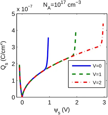
Figure 2.2: Total semiconductor charge density with different values for V, defined in the paragraph above equation (2.10).
forψs >0 and positive otherwise. The form ofQ0s written below is taken from [16]. Slightly different forms can be obtained that produce imaginary results around flatband [29, 30].
Q0s=∓p2qNAεs
h
ψs+φt
e−ψs/φt−1+
φte−(V+2φF)/φt
eψs/φt−1i1/2 (2.12)
2.2
The surface potential equation
While an explicit expression for the total semiconductor charge has been found, it is in terms of surface potential, not the applied gate bias. To relate band-bending with gate bias one writes an equation balancing all charges, an equation balancing all potentials, and applies Gauss’s Law to an ideal charge-free oxide [28]. Treating the oxide as charge-free is the same as assuming all oxide charge appears at the semiconductor interface.
Q0G+Q0s+Q0ox=0
VGB=φms+ψs+ψox
Q0G=Cox0 ψox
(2.13)
The charges to be balanced include the gate charge, semiconductor charge, and oxide charge. The oxide charge contains contributions from interface states and any fixed/trapped charge, labeled asQ0it andQ0o. Interface states are bias-dependent and have a value at flatband denotedQit00, which is the interface state charge density evaluated at zero band-bending and zero imref splitting. Combination of all equations results in a transcendental equation.
VGB=VFB+ψs−
Q0it(ψs)−Qit00
Cox0 − Q0s
Cox0 (2.14)
Equation (2.14) is the “surface potential equation” (SPE) following the terminology of [15].
The flatband voltage describes the voltage at which ψs =0 and there is no net semicon-ductor charge. Composed of oxide charge and the metal-semiconsemicon-ductor work function, it is the condition for flat energy bands and equilibrium-like conditions in the substrate. The metal-semiconductor work function can be calculated assuming a metal gate with known work func-tionφm. The semiconductor work function is the energy required to move an electron from the Fermi level to vacuum. Easily visualized by drawing a band diagram, it is expressed in terms of the substrate’s electron affinity, band gap, and Fermi level.
VFB=φms−
Q0o Cox0 −
Q0it00
Cox0 (2.15)
The SPE maps gate voltage to band-bending, and a unique mapping exists for every value of oxide thickness and doping. Interface states also distort this mapping and delay the onset of inversion by balancing gate charge along with semiconductor charge. Ignoring contributions fromQ0it someψs versusVGB curves can be generated. ψs(VGB)is plotted for different oxide thicknesses and doping in Figures 2.3a and 2.3b. Surface potential was calculated from−0.1V to 2φF +5φt for each curve. The surface potential increases almost linearly upward from flatband until inversion is reached, at which pointψs begins to saturate. This occurs because the inversion charge density increases rapidly and dominates the SPE. For the same bulk doping concentration different oxide thicknesses delay threshold as shown in 2.3(a). In 2.3(b), larger p-type doping moves the bulk Fermi level towards the valence band, requiring greater band bending to reach inversion.
−4 −2 0 2 4 6 8 −0.2 0 0.2 0.4 0.6 0.8 1 V GB (V) ψ s
(V)
NA=1017 cm−3
10 nm
30 nm 50 nm
(a)
−4 −2 0 2 4 6 8
−0.2 0 0.2 0.4 0.6 0.8 1 V GB (V) ψ s
(V)
tox = 30 nm
1016 1017 5x10¹⁶
(b)
−2 0 2 4 6
0 0.5 1 1.5 2 2.5 3 V GB (V) ψ s
(V)
N A=10
17
cm−3, t
ox=30 nm
2 V
1 V
0 V
(c)
2.3
Quantum mechanical effects
Band-bending at the insulator-semiconductor surface caused by an applied gate bias confines free carriers in a potential well at discrete energy levels above the conduction band. The den-sity and spatial distribution of free carriers are determined by numerical analysis of the coupled Schrodinger and Poisson equations, a computationally lengthy process unsuitable for a com-pact model. Quantum confinement requires more band-bending to achieve the same inversion charge density, a consequence of the lowest allowed energy level being some finite energy above Ec. Also, the distance from the interface to the centroid of the minority carrier distri-bution is slightly different from the classical result, giving an effective increase in the oxide capacitance density. The effects of quantum confinement are readily observed for devices with thin oxides and/or high doping: on a plot of gate capacitance versus voltage the peak capaci-tance fails to reachCox0 and the threshold’s magnitude increases [32].
Approximations for the lowest populated subband’s energy level can be found by either treating the potential well as triangular or assuming only the lowest subband is filled [20]. These approximations can be used to create an energy offset relative to the conduction band. The van Dort model considers quantum confinement as an effective bias-dependent bandgap widening term [33]. The intrinsic carrier concentration is replaced with a quantum mechanical version with energy gap offset, ∆E, proportional to the surface field raised to the two-thirds
power. However, the effective mass used in the computation of∆E loses some physical
mean-ing since more than one subband is involved [34]. A more physical approach would include more than one subband.
tri-angular well approximation has been found to be useful as a means of developing a bandgap widening term [35]. However, implementing the widening term for majority carriers can be cumbersome, because re-writing the semiconductor charge density in equation (2.12) while including such a term results in an ill-conditioned expression near flatband.
The triangular approximation has been shown to be accurate for determining minority car-rier and capacitance densities as a function of gate bias if more than one subband is considered [36]. Recently, it has been shown that the triangular assumption can result in an analytical expression for surface potential while considering many subbands [37]. The derivation con-tained in [37] is outlined and the important points presented since it will be used for quantum mechanical analysis of thin oxide devices in a later chapter.
Beginning from Poisson’s equation one immediately separates the contribution from mi-nority carriers. After multiplying both sides bydψ/dyand integrating throughout the bulk the integral of minority carriers is considered separately. The average value of the electric field in the inversion layer (E =−(Q0s+Q0i/2)/εs) is used to approximate the integral of minority carriers, that in turn allows for calculation of the surface field. The result contained below, im-plied by [37], could have been formulated by assumingQ0s=Q0i+Q0bwithQ0bequal to equation (2.12) devoid of contributions from minority carriers.
Q0s=Q0i−sign(ψs)
p
2qNAεs
h
φt
e−ψ/φt−1+ ψs
i1/2
(2.16)
the higher valley (four-fold degeneracy). The quantitiesmzL andmzH are the normal masses, valued at 0.916m0in the lower valley and 0.190m0in the higher valley [20]. In the proceeding equation,EFnis the quasi-Fermi level, andEi j are energy levels corresponding to the different subbands.
Q0i=−qkT
πh¯2
∑
igimdi
∑
j ln
1+e(EFn−Ei j)/kT
(2.17)
The energy levels given byEi j are eigenvalues resulting from the triangular well solution of Schrodinger’s equation. They are referenced to the location of the conduction band edge at the surface,Ec0, since in the solution of Schrodinger’s equation the bottom of the well is assumed to be at zero energy.
Ei j=Ec0+
¯
h2
2mzL
1/3
3πq
2 (j+3/4)E
2/3
(2.18)
The average value of the electric field in the quantum well, E, is technically in terms of
Q0i, but replacing it with the surface field multiplied by a coefficient allows for straightforward numerical search for surface potential. η is a coefficient found by [37] to be approximately 1.1. The straightforward numerical search is made possible by replacing−Q0s with Q0g+Q0ox
and using Gauss’s Law, which can be obtained from the relations supporting the SPE.
E≈Es
η (2.19)
=C
0
ox(VGB−VFB−ψs) +Q0it−Qit00
η εs
The difference EFn−Ei j in equation (2.17) can be written in terms of surface potential. Knowing that EFn =EF −qV and Ec0= Ec−qψs gives the desired result. The difference between bulk conduction and Fermi levels, Ec−EF, is equal to kTln(Nc/ni) +qφF with Nc being the effective conduction band density of states. It can be approximated asEg/2+qφF.
EFn−Ei j =qψs−qV−
¯
h2
2mzL 1/3
3πq
2 (j+3/4)E
2/3
−kTln(Nc/ni)−qφF (2.21)
The above equations form the core of the analytical approximation derived in [37]. In this research work interface charge density has been included in equation (2.20) and directly affects the subbands’ energy levels. This is the only modification needed to include interface states in the one-dimensional solution of Poisson’s equation while considering quantum confinement of minority carriers.
0 1 2 3 4 0 0.2 0.4 0.6 0.8 1
VGB−VFB (V)
C GB / C ox N A=10 16 cm−3, t
ox=2.5nm
Classical QM
(a)
0 1 2 3 4
0 0.2 0.4 0.6 0.8 1
VGB−VFB (V)
C GB / C ox N A=10 16 cm−3, t
ox=25nm
Classical QM
(b)
0 1 2 3 4
0 0.2 0.4 0.6 0.8 1
VGB−VFB (V)
C GB
/ C
ox
NA=1016cm−3, tox=50nm
Classical QM
(c)
2.3.1
Modifications for inversion in p-channel MOS devices
The semiconductor charge density in (2.16) changes to accommodate holes as they become minority carriers in a substrate of uniform n-type doping. The quantum confinement of accu-mulated majority carriers is again ignored.
Q0s=Q0i−sign(ψs)
p
2qNDεs
h
φt
eψ/φt−1− ψs
i1/2
(2.22)
The inversion charge density, now comprised of holes, is evaluated differently since there are three hole bands: the light hole, heavy hole, and split-off bands. The indexitakes on values
L, H, andScorresponding to the three hole bands. Index j is the “rung on the energy ladder” where higher index values contribute a smaller portion to the total inversion charge density. These comments are made based on information contained in [38], which also contains the quantization and density of states effective masses for the (100) silicon surface. The total charge density is taken to be unchanged relative to the nMOS case except for the sign and argument in the exponential. Also, the split-off band has a constant energy difference between the two other bands, which must be accounted for when calculating charge [38].
Q0i=qkT
πh¯2
∑
igimdi
∑
j ln
1+e(Ei j−EF p)/kT
(2.23)
case in (2.18).
Ei j=Ev0−
¯
h2
2mzL
1/3
3πq
2 (j+3/4)E
2/3
(2.24)
The difference between an energy levelEi j and the quasi-Fermi level also changes slightly. Knowing that EF p =EF −qV and Ev0 =Ev−qψs gives the desired result. The difference between bulk valence and Fermi levels, Ev−EF, is equal to −kTln(Nv/ni) +qφF with Nv being the effective valence band density of states. It can be approximated asEg/2+qφF.
Ei j−EF p=−qψs+qV−
¯
h2
2mzL 1/3
3πq
2 (j+3/4)E
2/3
−kTln(Nv/ni) +qφF (2.25)
2.3.2
Summary of useful charge density expressions
2.4
Interface trapped charge
In any semiconductor device involving an insulator there are undesirable charges introduced that shift the flatband voltage, cause hysteresis of measured data, and/or modify the induced channel charge. These all manifest as a shift in the ideal flatband voltage and with the exception of surface traps do not contribute any capacitance. Insulator-related charges are categorized as: fixed, trapped, interface trap, and mobile [6]. Mobile charge produces CV hysteresis and its variation with applied voltage will be ignored.
For the purposes of modeling, a detailed understanding of fixed/trapped charge is not nec-essary since all appear as a shift in the flatband voltage and can be effectively lumped into the term Q0o/Cox0 . In contrast, of great interest is understanding interface traps since these charge/discharge with varying bias and can significantly affect device performance. In a sim-ple capacitor, interface traps shift the flatband voltage and distort capacitance-voltage measure-ments depending on the frequency. An example diagram of interface trap occupation is shown in Figure 2.5, re-drawn from [39].
EF Ev Ei Ec
filled states empty states
qVgb
2.4.1
Trap occupation
Interface states are continually distributed throughout the bandgap and are described with den-sityDit(E)and probability of occupationF(E). The probability of occupation varies with band bending and quasi Fermi level but is much different between the two cases of thermal equilib-rium and steady-state. For thermal equilibequilib-rium the MOS device’s trap occupation function approaches a simplified form, labeled Fo(E). The equilibrium Fo(E) was used by Nicollian and Brews to develop MOS capacitor admittance equations for interface state analysis [6].
However, a MOSFET operating under steady-state conditions can potentially have a quasi Fermi level quite different from the bulk Fermi level owing to carrier injection from the source. The inclusion of the quasi Fermi level precludes the use of Fo(E). Instead, the steady-state occupation functionF(E)is needed for interface trapped charge calculations unless the model is declared in advance to have limitations. The equilibrium occupation function is only valid if the amount of imref splitting is kept small relative to the surface potential. P. Muls used this limitation to investigate trap-affected MOSFET behavior in weak inversion [7].
The steady-state trap occupation probability can be given following the Shockley/Read [40] and Hall [41] formulation. The occupation function at the surface can be found if the equations are modified slightly to incorporate band-bending [27]. The usual means of writing carrier cap-ture/emission rates involves constants of proportionality, filled/empty trap densities, and carrier concentration. The carrier concentrations are typically written in terms of Maxwell-Boltzmann statistics, and the steady-state trap occupation function reflects this by being composed of ex-ponentials [7].
F(E) = 1+ e
(Ei−EF−qψs)/kT+e(E−Ei)/kT
e(EF−Ei+qψs−qV)/kT+e(Ei−E)/kT
!−1
0 0.5 1 1.5 0
0.2 0.4 0.6 0.8 1
E−E v (eV)
occupation probability
V = 0
ψs=φ F
ψs=2φ F
(a)
0 0.5 1 1.5
0 0.2 0.4 0.6 0.8 1
E−E v (eV)
occupation probability
V = 0.3
F(E) F
FD(E)
ψs=2φ F ψs=φF
(b)
Figure 2.6: Difference in occupation functions whereF is the exact steady-state version and
FFD is the simplified quasi Fermi-Dirac version. The exact version indicates thatV can only push the falling edge leftward until around midgap, at which point the simplified version be-comes incorrect.
The above reduces only for smallV to become a quasi Fermi-Dirac distribution [7].
FFD(E) =1+e(E−EF−ψs+qV)/kT−1 (2.27)
2.4.2
Interface trapped charge density
The total interface trapped charge involves an integral throughout the bandgap of the density functionDit(E)multiplied with F(E) [6]. In the derivation of (2.26) it was assumed that the traps were acceptor-like. If they had been assumed donor-like, the occupation function would simply be 1−F(E), whereF(E)is from (2.26).
Q0it,d=q
Z Ec
Ev
[1−F(E)]Dit,d(E)dE (2.28)
Q0it,a=−q
Z Ec
Ev
F(E)Dit,a(E)dE (2.29)
Distinguishing between the acceptor-like and donor-like densities is deemed unimportant in this work. This is because an important observation can be made ifQ0it is described as the sum ofQ0it,d andQ0it,a.
Q0it(ψs) =q Z Ec
Ev
Dit,ddE−q
Z Ec
Ev
F(E)(Dit,d+Dit,a)dE (2.30)
The first integral is actually bias-independent, and only shows up as a shift in the flatband voltage. The sumDit,d+Dit,ais determined from measurements and is labeledDit. Therefore, from a modeling perspective, all traps can be treated as acceptor-like and the flatband voltage left as a measured quantity.
Q0it ≈ −q
Z ψs+EF−V
Ev
Dit(E)dET (2.31)
One immediate limitation of (2.31) is thatF(E)temperature dependence is lost. Also, high levels of Dit (roughly>1012 cm−2eV−1) are not modeled well by this approximation unless the upper limit of integration is kept from exceedingEc. Ignoring this boundary will result in an incorrect surface potential in strong inversion, leading to an incorrect inversion charge density, leading to an incorrect drain current. Low levels ofDit can make use of this simplification since when the simplification is in error semiconductor charge density is dominant and interface trapping is not important. Also, (2.31) is incorrect for determining surface potential below weak inversion whenever imref splitting is included in the SPE because of the differences between (2.26) and (2.27). Consequently, equation (2.31) cannot be used for accuracy and more precise approximations to (2.30) will be generated.
Some comments regarding Dit(E) must be made first. It has been found experimentally that interface trap density can have a U-like distribution over the bandgap with peaks at the band edges. A function that empirically describes this behavior uses two exponentials which decay towards a midgap density [42]. The rate of decay is controlled by the bandtail parameter, denoted asb.
Dit(E) =Dve−(E−Ev)/bv+Di+Dce(E−Ec)/bc (2.32)
signifi-cant effects in plots of drain current, the exact details of which are left for a later section. In regards to drain current only Di and the minority carrier bandtail are important. As an example, an n-channel MOSFET at the onset of weak inversion has ψs=φF and roughly all states below midgap are occupied. Assuming the Dve−(E−Ev)/b term has dropped below
Di then contributions from the valence bandtail have saturated. Therefore, for an n-channel MOSFET only two terms from (2.32) are needed to capture the effects of interface states on drain current. The ignored term simply shifts the flatband voltage. For capacitance simulation from accumulation through strong inversion all terms would be needed. Example plots ofDit
and the resultingQ0it are shown in Figures 2.7 and 2.8.
Dit(E) =Di+Dce(E−Ec)/b (2.33)
0 0.5 1 1012
1013
E−Ev (eV)
D it (cm −2 eV −1 ) D i=10 12 , D c=10 13 b=0.1 eV b=0.05 b=0.01 (a)
−0.5 0 0.5 1 1.5
−4 −3 −2 −1
0x 10
−7
ψs (V)
Q it (C/cm 2 ) D i=10 12 , D c=10 13 (b)
Figure 2.7: Effect of bandtail parameter bon interface state charge density. Without theDc
termQ0itwould increase linearly with respect toψsand then saturate asEcis bent down towards
EF.V =0.
0 0.5 1
1011 1012 1013 1014
E−E v (eV) D it (cm −2 eV −1 ) b=0.05 eV D i=2x10
12, D c=5x10 13 D i=10 12 , D c=10 13 D i=5x10
11, D c=1x10
12
(a)
−0.5 0 0.5 1 1.5
−8 −6 −4 −2
0x 10
−7
ψs (V)
Q it
(C/cm
2 )
b=0.05 eV
(b)
0 5 10 −0.2 0 0.2 0.4 0.6 0.8 1
Di=1012, Dc=1013
VGB (V)
ψ s (V) b=0.1 eV b=0.05 b=0.01 (a)
0 5 10
−0.2 0 0.2 0.4 0.6 0.8 1 b=0.05 eV
VGB (V)
ψ s
(V)
(b)
0 5 10
0 0.5 1 1.5 2 2.5 3 V GB (V) ψ s
(V)
Di=1012, Dc=1013, b=0.05
V=0
V=1
V=2
(c)
2.4.3
Approximating trapped charge density
Because of equation (2.32) the interface trapped charge density becomes split into three com-ponents. None are integrable with the steady-stateF(E)but approximations are possible. The flatband-contributing offset in (2.30) is ignored since it has no bias dependence.
Q0it=VAL+MID+CON (2.34)
VAL=−qDv Z Ec
Ev
e−(E−Ev)/bF(E)dE (2.35)
MID=−qDi
Z Ec
Ev
F(E)dE (2.36)
CON=−qDc
Z Ec
Ev
e(E−Ec)/bF(E)dE (2.37)
The midgap density integral can be accurately approximated by observing graphically its derivative with respect to surface potential. The proposed solution is to use a summation of Fermi functions.
dMID
dψs ≈ −
qDi
1
1+e−(ψs−(Ev−EF))/kT −
1
1+e−(ψs−(Ei−EF))/kT
+ 1
1+e−(ψs−(Ei−EF+V))/kT −
1
1+e−(ψs−(Ec−EF+V))/kT
(2.38)
0 0.5 1 1.5 −2
−1.5 −1 −0.5
0x 10
−8 Di=1011, Dc=0
ψs (V)
Q it
(C/cm
2 ) 0.2 0.4 0.6 0.8 1
0 0.5
% error
V=0.5
V=0
Figure 2.10: Quality of MID. Solid line: developed approximation; closed circles: exact result. Inset shows percent error forV =0.5 since forV =0 the result is exact. The percent error is the same for other values ofV.
MID≈ −qDiEg+qDiVTln
1+e−(ψs−Ei+EF)/kT 1+e−(ψs−Ec+EF−V)/kT 1+e−(ψs−Ev+EF)/kT
1+e−(ψs−Ei+EF−V)/kT
(2.39)
The quality of MID is imperfect away from theV =0 case. When the surface potential equals φF or φF+V the integral of the steady-state occupation function undergoes a rapid transition that is not captured perfectly by the MID approximation. Relative error peaks around half a percent (Figure 2.10), which is undesirable. However, it is tolerable because inversion charge density is very small around these two points (φF+V being onset of weak inversion). This peak value is independent ofDiandV but it is a function of temperature.
Fermi-Dirac version. At large values ofV where the quasi Fermi-Dirac occupation function is in error, the contribution from CON is usually negligible relative to that of MID assumingDi is only around a hundredth ofDc. However, whenb becomes large (roughly 0.1 eV and above) the quasi-Fermi-Dirac occupation function can give significant error whenV > 0 and therefore cannot be used.
Any approximation to CON must be precise because inversion charge density is very sen-sitive to small changes in surface potential. For this reason the integral associated with CON is approximated by discrete integration. Applying the trapezoidal rule requires the integrand be generated for many datapoints, typically around 1000 for relative error below 0.01%. Such a large number of points slows down the numerical search forψsin the SPE increasing model computation time. A solution is to successively apply integration by parts.
CON=σ+ N
∑
k=0(−1)kbk+1e(E−Ec)/bF(k)
Ec
Ev (2.40)
σ = (−b)N+1 Z Ec
Ev
e(E−Ec)/bF(N+1)dE (2.41)
The superscript attached to F in parenthesis indicates the derivative of order k. σ is the remaining integral after integration by parts is appliedN times. It is dominant when b>VT
and the Fermi level is below the conduction band edge. When b <VT it is small and the summation converges more rapidly to the actual integral.
0 0.5 1 1.5 −2
−1.5 −1 −0.5
0x 10
−7 Di=1011, Dc=1013
ψs (V)
Q it
(C/cm
2 )
(a)
0.8 0.9 1 1.1
0 0.05 0.1 0.15
ψs (V)
% error
D i=10
11 , D
c=10 13
, V=0
b=0.1 eV
b=0.05
b=0.01
(b)
Figure 2.11: Magnitude of error associated with the summation and σ integration approach forV =0. As the ratioDi/Dc is increased the error will decrease.V =0 andT =25C. All of the error is from CON because MID is exact atV =0.
than the trapezoidal rule forσ. The reason that Simpson’s rule is not just applied to the inte-grand of CON is because the inteinte-grand’s behavior versusE is significantly different depending on whetherbis greater or less thankT. The summation andσ take turns being the dominant component of CON depending onband bias.
0 0.5 1 1.5 2 −2
−1.5 −1 −0.5
0x 10
−7
ψs (V)
Q it (C/cm 2 ) D i=10 11 , D c=10 13 (a)
0 0.5 1 1.5 2
0 0.1 0.2 0.3 0.4 0.5
ψs (V)
% error D i=10 11 , D c=10 13 , V=0.5 b=0.1 eV b=0.05 b=0.01 (b)
Figure 2.12: Magnitude of error associated with the summation and σ integration approach forV =0.5. As the ratioDi/Dcis increased the error will decrease.
0.8 0.9 1 1.1
−2 −1 0 1 2
ψs (V)
V GB,exact
−V
GB,approx
(mV)
Di=1011, Dc=1013, V=0
b=0.1 eV
b=0.05
b=0.01
(a)
0.5 1 1.5
−2 −1 0 1 2
Di=1011, Dc=1013, V=0.5
ψs (V)
V GB,exact −V GB,approx (mV) b=0.1 eV b=0.05 b=0.01 (b)
Figure 2.13: Delta in predicted gate-bulk voltage by evaluating SPE attox=30nm. Increasing
2.4.4
Expanding
Q
0itExact analytical computation of drain current is impossible when the effects of interface states are included. order expansions are invariably required meaning that the first through Nth-order derivative of Qit must be known. In this work second order expansions of V must be computed, thus the first and second derivatives of MID and CON are considered.
The first derivative ofQ0it is the interface state capacitance as f →0 Hz. It is commonly approximated away from the band edges (for a MOS capacitor).
Cit =−
dQ0it dψs
(2.42)
≈Dit(ψs+EF). (2.43)
However, the above result is not very useful for all biases since Q0it saturates near the band edges. More importantly, high levels ofDitobviate its use. If the magnitude ofDit is small then the region where the above approximation is invalid is also the region whereCit is dwarfed by semiconductor capacitance. So, the fact that it is invalid is unimportant for lowDit. However, for high densities of interface states (particularly near the band edge) none of this is true. For this reason more exact expressions are utilized.
dMID
dψs ≈ −
qDi
θm1−θm2
dV dψs
(2.44)
θm1=
1
1+e(Ev−qψs−EF)/kT −
1
1+e(Ei−qψs−EF)/kT
+ 1
1+e(Ei−qψs−EF+qV)/kT −
1
1+e(Ec−qψs−EF+qV)/kT
(2.45)
θm2=
1
1+e(Ei−qψs−EF+qV)/kT −
1
1+e(Ec−qψs−EF+qV)/kT (2.46)
Derivatives of CON are evaluted by distributing d/dψs into the integral. Integration by parts is not applied becausedF/dψs·e(E−Ec)/bis more accurately discretely integrated over a small number of points than isF·e(E−Ec)/b.
dCON
dψs
=−qDc
φt
θc1−θc2
dV dψs
(2.47)
θc1=
Z Ec
Ev
e(E−Ec)/b
e(EF−Ei+qψs−qV)/kTB−A B2 +e
(Ei−EF−qψs)/kT A
B2
dE (2.48)
θc2=
Z Ec
Ev
e(E−Ec)/be(EF−Ei+qψs−qV)/kTB−A
B2 dE (2.49)
FunctionsAandBare the numerator and denominator of the steady-state occupation function.
A=e(EF−Ei+qψs−qV)/kT+e(Ei−E)/kT (2.50)
B=A+e(Ei−EF−qψs)/kT+e(E−Ei)/kT (2.51)
0 0.5 1 1.5 0 0.2 0.4 0.6 0.8
1x 10
−6
ψs (V)
−dQ it /d ψ s (F/cm 2 ) D i=10 11 , D c=10 13 b=0.1 eV b=0.05 b=0.01 (a)
0.6 0.8 1 1.2
0 1 2 3 4 5 6
x 1012
qψs+EF−Ev (eV)
−dQ it /d ψ s /q (cm −2 eV −1 ) D i=10 11 , D c=10 13 (b)
Figure 2.14: First derivative ofQ0it forV =0 (MOS capacitor case). In (b) each solid exponen-tial line is a plot ofDi+Dce(ψs+EF−Ec)/bto investigate the common approximationCit/q≈Dit. The x-axis can be thought of asE−Evsimilar to Figure 2.7.
three curves. In Figure 2.14b the validity ofCit/q≈Dit is examined. The approximation works well for large values ofbbut fails whenbis near or belowφt.
The reason the approximation fails for b<φt when −dQ0it/dψs rises toward its peak can be explained by considering the integrand of CON. IfV =0 then a first order expansion about
E=Ecgives a good approximation to the integrand, particularly forb<φt.
e(E−Ec)/b·FFD≈e(E−Ec)/b "
1
1+e(Ec−EF−qψs)/kT − 1
kT
e(Ec−EF−qψs)/kT
1+e(Ec−EF−qψs)/kT2(E−Ec) #
(2.52)
approximated as a simple exponential.
e(E−Ec)/b·FFD≈e(E−Ec)/be−(E−EF−qψs)/kT (2.53)
Chapter 3
Drain current
A flow of carriers from drain to source caused by an applied drain-source bias is associated with a gradient in the quasi-Fermi level as a function of position in the channel. Departing from the source, minority carriers flow towards the drain over a distance, L, in what can be assumed to be a current density that is constant across the channel width, W. The voltage applied to the gate electrode controls the current passing through the device and is related to the system of internal charges by the surface potential equation. The expression for the laminar flow of current in MOSFET compact models is usually taken to be,
Ids=−µW Q0idψs
dx +µWVT dQ0i
dx , (3.1)
Ids=−µW Q0idV
dx (3.2)
Equation (3.1) is referred to as “drift-diffusion” and becomes an approximation of equation (3.2) in a charge sheet model [16, 43]. “Exact” one-dimensional solution of (3.2) is performed numerically and is commonly referred to as the Pao-Sah double integral. It being computation-ally slow to evaluate, the double integral is primarily useful for gauging model error. Equation (3.2) can become a double integral depending on howQ0iis evaluated. Classically, it is found by integration of the minority carrier charge density from the surface to deep in the bulk. Know-ing thatdψs/dy=−E, a change of variables can be performed whereE is known analytically from one of the steps used to establish (2.12). For an n-channel FET, the minority carriers are electrons.
Q0i=−qNA
Z ψs
0
e(ψ−2φF−V)/φt
E(ψ)
dψ (3.3)
Therefore, the exact expression for current that the final compact model can be compared against is the following double integral [16]. The influence of interface states is not explicit but is contained within the surface potential equation that relatesV,ψs, andVGB.
Ids=qNAW L
Z VDB
VSB Z ψs
0
e(ψ−2φF−V)/φt
E(ψ) dψdV (3.4)
over which ψs drops a negligible amount. This allows for the separation of Q0s into inversion and depletion components. Doing so generally allows for analytical integration (at least when ignoring interface states) of Q0i and therefore an analytical expression for drain current. It is the supporting assumption for the classic “charge sheet model” [44] and is an integral part of surface potential models. The depletion, or “bulk,” charge is found in the same manner asQ0s
is derived, but with a charge density,ρ, devoid of minority carriers. Inversion charge density is given as the difference betweenQ0sandQ0b.
Q0b=∓p2qNAεs
h
ψsφt
e−ψs/φt−1i1/2 (3.5)
If the carriers are not treated classically then the QM expression for inversion charge density in Chapter 2 can be used. The drain current expressions developed below are understood to still be valid provided surface potential andQ0iare calculated appropriately.
3.1
Charge Sheet Approximation details
IfQ0sis given as the sum ofQ0iandQ0b, thenQ0ican be evaluated in three ways. The first method is simply by computing the differenceQ0s−Q0b. A more common approach is by rearranging the SPE.
Q0i=Cox0
VFB+ψs−VGB−
Q0b+Q0it−Q0it00 Cox0
(3.6)
it is difficult to be numerically precise in the calculation of Q0i with (3.6) since the quantity in parenthesis invariably involves finding the difference of two very similar values. Precise calculation of inversion charge density is necessary to calculate low current levels. By multi-plyingQ0s−Q0b by a fraction equal to unity with numerator/denominator equal toQ0s+Q0b, the following expression is obtained [16].
Q0i=2qεsNAφt
e−(V+2φF)/φteψs/φt−1
Q0s+Q0b (3.7)
Since inversion charge density varies over many orders of magnitude from subthreshold to strong inversion, equation (3.7) is preferred.
Of course, assuming that the depletion region experiences the full ψs drop is not totally correct. What matters is to what degree the assumption is incorrect. The exact computation ofQ0iinvolves an integration as written in (3.3). A similar integral can be written for the bulk charge wheree(ψ−2φF−V)/φt is replaced by 1−e−ψ/φt. The vertical electric field,E, is simply −Qs/ε evaluated at an arbitraryψ instead ofψs.
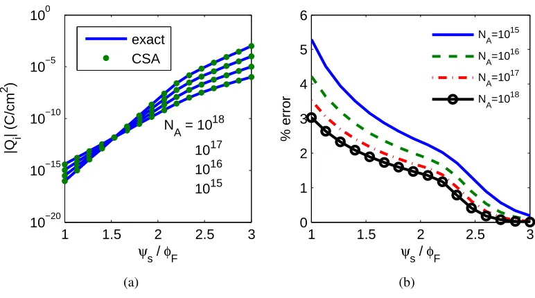
1 1.5 2 2.5 3 10−20
10−15 10−10 10−5 100
ψs / φF
|Q
i
| (C/cm
2 )
exact CSA
N A = 10
18
1017 1016 1015
(a)
1 1.5 2 2.5 3
0 1 2 3 4 5 6
ψs / φF
% error
NA=1015
N A=10
16
N A=10
17
N A=10
18
(b)
As shown in Figures 3.1a-b some doping and bias-dependent error is unavoidably included by making the charge sheet approximation. More error is included by using the drift-diffusion equation for Ids contained in (3.1). In the context of a charge sheet model the difference be-tween (3.1) and (3.2) also contributes some error, since there is some amount of approximation involved in the statement thatdQ0i/dψs=Q0i/φt[1−dV/dψs]. Adding in interface states to the mix further compounds the situation and two plots are created to gauge the usefulness of (3.1) in Figure 3.2.