KIRKPATRICK, CASEY JOE. Gate Stack Design for Threshold Voltage Control of Gallium Nitride Power Transistors. (Under the direction of Dr. Veena Misra).
Gallium Nitride is an excellent material for power semiconductor applications due to its wide band gap, good thermal conductivity, high mobility and high breakdown field. The
availability of high quality GaN on silicon substrates promotes GaN as a future low cost, high power semiconductor material. However, there are still challenges that need to be overcome before AlGaN/GaN devices can provide robust solutions for power applications.
Particularly challenging, is that high mobility GaN transistors are normally-on, which requires a negative gate bias to turn off devices. A gate stack design to enable enhancement mode operation of GaN transistor devices has been developed. Gate dielectrics to reduce losses due to leakage deposited by atomic layer deposition have been characterized and evaluated. SiO2 and HfAlO deposited by atomic layer deposition on GaN have been
characterized electrically for the first time. The band alignment of these dielectrics with GaN as well as commonly used Al2O3 and HfO2 dielectrics has also been experimentally
by
Casey Joe Kirkpatrick
A dissertation submitted to the Graduate Faculty of North Carolina State University
in partial fulfillment of the requirements for the degree of
Doctor of Philosophy
Electrical Engineering
Raleigh, North Carolina 2013
APPROVED BY:
_______________________________ ______________________________
Dr. Veena Misra Dr. Alex Huang
Committee Chair
________________________________ ________________________________
DEDICATION
BIOGRAPHY
Casey Kirkpatrick was born in Hannibal, New York on June 17th 1987. As an undergraduate at North Carolina State University, Casey worked under Dr. Mehmet Ozturk on Hall Effect characterization tools and strained SiGe contacts. In 2008, Casey participated in the National Science Foundation’s research experience for undergraduates (REU) program at the Johns
ACKNOWLEDGMENTS
I couldn’t have got to this point without the help and support of my colleagues and
friends. I first want to thank my advisor Veena Misra for everything she has done to guide this work and to build the exceptional group and environment I have had the privilege to work in. I also want thank Mehmet Ozturk who introduced me to semiconductor research so early in my undergraduate career and who introduced me to the Misra group. As an
undergraduate, I was helped immensely by Emre Alptekin who helped me get my first hands on experience. Thank you to Jeong-Hyun Cho who made a 10 week stint at the Johns
Hopkins University one of the most important things I did as an undergraduate. All of my fellow group members have given great feedback and discussion through the years. Steven Mills, Xiangyu Yang, Srikant Jayanti, Rahul Suri, Rebecca Thomas, Sarah Haney and Steven Novak have all been instrumental in making this happen. A special thanks to Narayanan Ramanan and Bongmook Lee who have worked so closely with me on GaN, as well as to Dan Lichtenwalner for helping me get a strong start working with wide band gap
semiconductors.
Thank you to the rest of my committee Dr. Huang and Dr. Sitar for taking the time to work with me and for excellent guidance, especially during my preliminary exam.
REU program and for making me even prouder of North Carolina State University with the new ASSIST center.
Thank you to my parents Joe and Yevette Kirkpatrick for their continued support. I also want to thank my grandma Mary Kirkpatrick for always being supportive and inquisitive of my research.
TABLE OF CONTENTS
LIST OF TABLES...…...………..………viii
LIST OF FIGURES….………...…..……..…ix
1 INTRODUCTION ... 1
1.1 Motivation ... 1
1.2 Gallium Nitride for Power Electronics... 2
1.3 Goals of the Following Work... 4
1.4 Document Preview... 4
2 DEVICE STRUCTURES, CHARACTERIZATION AND SIMULATION TECHNIQUES ... 7
2.1 Introduction to Chapter... 7
2.2 Atomic layer deposition ... 7
2.3 Back to Back Capacitor Structure ... 9
2.4 AlGaN/GaN transistor devices ... 10
2.5 Heterojunction Field Effect Transistor Operation ... 16
2.6 Electron Beam Lithography ... 25
2.7 Electrical characterization methods ... 28
2.8 Physical characterization ... 45
2.9 Simulation ... 47
3 PRELIMINARY GATE DIELECTRIC EVALUATION ... 49
3.1 Chapter Introduction ... 49
3.2 Surface Cleaning ... 49
3.3 Post Dielectric Annealing ... 52
3.4 Preliminary Electrical Evaluation ... 53
3.5 Band Alignment of ALD SiO2, HfAlO, HfO2 and Al2O3 ... 57
4 MOS-HFET DEVICES ... 65
4.1 Introduction to Chapter... 65
4.2 ALD SiO2 MOS-HFET Experimental ... 66
4.3 ALD SiO2 MOS-HFET Characteristics ... 67
4.5 ALD HfAlO and SiO2 Comparison ... 72
4.6 Technologies for Enhancement mode HFETs ... 75
4.7 Recessed Gate MOS-HFET ... 78
5 FLASH MOS-HFET... 80
5.1 Flash MOS-HFET introduction ... 80
5.2 Flash MOS-HFET Simulation ... 81
5.3 Flash MOS-HFET Fabrication ... 84
5.4 Flash MOS-HFET Charging and Memory Characteristics ... 86
5.5 Flash MOS-HFET High Power Considerations ... 89
5.6 Retention Improvement of the Flash MOS-HFET... 99
6 CIRCUIT CONTROL OF THE FLASH MOS-HFET ... 102
6.1 Introduction to Chapter... 102
6.2 Flash MOS-HFET Retention Conditions ... 103
6.3 Flash MOS-HFET Stability by Field Driven Feedback ... 105
6.4 Boost Converter Circuit with E-mode Flash MOS-HFET ... 108
6.5 Alternative Charging Methods ... 111
6.6 Flash MOS-HFET SFDF Conclusions ... 113
7 SCALING AND SCALABILITY FOR POWER MOS-HFETS ... 115
7.1 MOS-HFET Scaling by Electron Beam Lithography ... 115
7.2 Scalability of GaN Power HFETs ... 119
7.3 Practical MOS-HFET Scaling Limits ... 120
8 CONCLUSIONS AND FUTURE WORK ... 129
8.1 Conclusions ... 129
8.2 Future Work ... 131
8.3 GaN or SiC? A Perspective on the Future of Power Electronics ... 134
LIST OF TABLES
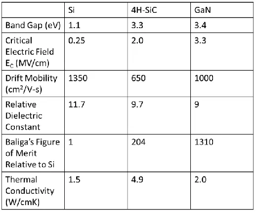
Table 1.1 Typical material values for Si, SiC and GaN... 2
Table 2.1 Material parameters for wafers from different vendors ... 14
Table 2.2 Spontaneous and piezoelectric polarization values ... 18
Table 2.3 Standard processes for commonly used resists ... 27
LIST OF FIGURES
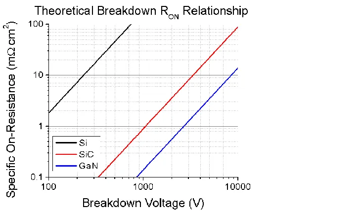
Figure 1.1 Theoretical on-resistance as a function of breakdown voltage ... 3
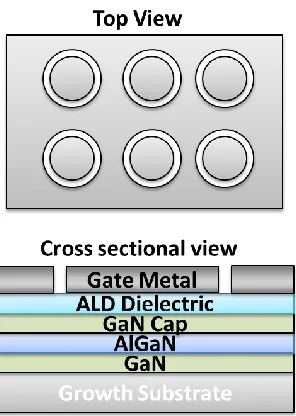
Figure 2.1 Top and cross-sectional view of a typical back to back capacitor structure ... 8
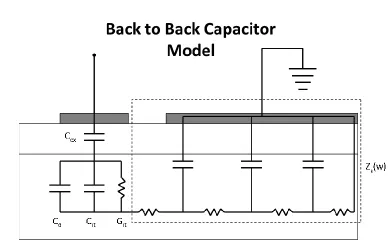
Figure 2.2 Equivalent circuit of the back to back capacitor ... 10
Figure 2.3 Partial GaN crystal illustration for visualization of polar atoms ... 11
Figure 2.4 Origin of the polarization in GaN ... 12
Figure 2.5 Illustration of the compensation of bound charge within a polarized material ... 13
Figure 2.6 Band diagram illustrating the 2DEG confinement ... 13
Figure 2.7 HFET and MOS-HFET structures with a GaN bulk layer ... 15
Figure 2.8 Pinch off condition ... 23
Figure 2.9 Ideal ID VD characteristics of an HFET ... 25
Figure 2.10 The effect of spacing between groups of devices on stitching ... 26
Figure 2.11 Typical Hall effect geometry and notation ... 34
Figure 2.12 Commercially available Ecopia HMS-3000 Hall effect sample holder ... 36
Figure 2.13 Proposed setup for Hall effect measurements. ... 39
Figure 2.14 Hall voltage measured as a function of time ... 43
Figure 2.15 Averaged slope of VHall for different magnetic fields. ... 45
Figure 3.1 Ga 2p3/2 spectra for the GaN surface before and after cleaning ... 49
Figure 3.2 Capacitance voltage characteristic at 1 MHz ... 51
Figure 3.4 Integration of the C-V profile for back to back capacitors ... 54
Figure 3.5 100 kHz capacitance voltage profile for Al2O3, HfAlO and SiO2 ... 54
Figure 3.6 Threshold voltage comparison from literature ... 55
Figure 3.7 Threshold voltage as a function of EOT. ... 56
Figure 3.9 XPS spectra for thin and thick dielectrics ... 61
Figure 3.10 Valence band spectra for clean substrate and each dielectric ... 62
Figure 3.11 O 1s energy loss spectra for band gap determination of each dielectric ... 63
Figure 3.12 Schematic band alignment for SiO2, Al2O3, HfO2 and HfAlO ... 64
Figure 4.1 Cross sectional TEM of the SiO2/GaN interface ... 66
Figure 4.2 O 1s (a) and Si 2p (b) XPS spectra ... 67
Figure 4.3 Electrical characteristics of MOS-HFET with 7 nm SiO2 ... 70
Figure 4.4 IDS VGS characteristics at VDS=250 mV. ... 72
Figure 4.5 IDS–VDS characteristics under DC and pulsed conditions. ... 73
Figure 4.6 Gate leakage current density comparison ... 74
Figure 4.7 MOS-HFET transconductances ... 75
Figure 4.8 Two dimensional electron gas concentration ... 76
Figure 4.9 Transfer I-V characteristics at Vds=1 V for 5nm gate recess ... 78
Figure 4.10 Output I-V characteristics for recessed gate transistor ... 79
Figure 5.1 Cross-sectional view of Flash MOS-HFET device ... 81
Figure 5.2 Synopsys TCAD structure for simulation of Flash MOS-HFET device ... 81
Figure 5.4 Conduction band profile before and after charging ... 83
Figure 5.5 Simulated sheet charge concentration as a function of charging time ... 84
Figure 5.6 Band diagram illustrating the energy bands of the blocking dielectric ... 84
Figure 5.7 ID-VD characteristics for Flash MOS-HFET devices before charging ... 86
Figure 5.8 Threshold voltage shift with increasing programming voltage ... 86
Figure 5.9 Nearly parallel shift in transconductance ... 87
Figure 5.10 Shift in CV curves before and after programing ... 88
Figure 5.11 Threshold voltage as a function of charging time ... 87
Figure 5.12 Retention characteristics ... 89
Figure 5.13 Reduced barrier to tunneling for trapped electrons ... 90
Figure 5.14 Basic device characteristics ... 92
Figure 5.15 Gate leakage before and after programming ... 93
Figure 5.16 Threshold voltage shift with increasing charging voltage ... 94
Figure 5.17 Threshold voltage shift with increasing charging time ... 95
Figure 5.18 Threshold voltage as a function of elapsed time from charging ... 96
Figure 5.19 Threshold voltage shift after drain stressing for 30 s ... 97
Figure 5.20 Retention measurements at increased temperature ... 98
Figure 5.21 Improved Retention Characteristics ... 99
Figure 6.1 Change in threshold voltage for the active and passive conditions ... 104
Figure 6.2 Simulated band diagram for the Flash MOS-HFET ... 105
Figure 6.4 Circuit model of constructed boost converter circuit ... 108
Figure 6.5 Simulated output voltage for constructed boost converter ... 109
Figure 6.6 Boost converter input and output as a function of time ... 110
Figure 6.7 Threshold voltage remains stable ... 111
Figure 6.8 charginge by applying gate bias at the operating voltage and frequency. ... 112
Figure 6.9 Charging by applying a low frequency pulse followed by the operating pulse .. 113
Figure 7.1 SEM image of fabricated MOS-HFET ... 115
Figure 7.2 ID-VG characteristics for a 150 nm LG………..117
Figure 7.3 ID-VD characteristics for devices with a gate length of 150 nm. ... 116
Figure 7.4 SEM image of a 1A MOS-HFET device ... 118
Figure 7.5 RON as a function of LGD for devices fabricated by electron beam lithography .. 119
Figure 7.6 HFET breakdown voltage taken at a drain current of 0.1 mA/mm ... 122
Figure 7.7 Decreasing gate length makes the threshold voltage more negatived ... 125
Figure 7.8 As the drain voltage is increased, threshold voltage decreases ... 126
Figure 7.9 Expected RON for a combination of state of the art technologies ... 127
1
INTRODUCTION
1.1 Motivation
Power electronics are critical in enabling efficient energy distribution from
generation, such as at power plant or a wind mill, to consumption. Energy is converted by power electronic devices several times from high to low voltage and vice versa before it reaches its final destination such as a computer chip or a wall socket. In order to meet the rapidly increasing energy needs of our society in a sustainable and environmentally responsible manner, intelligent, efficient energy conversion is required. For low voltage conversion applications (<600), Si solid state power converters are conventionally applied. Si devices have reached their theoretical limit for efficient operation, and cannot be applied for higher voltage applications efficiently. This has led to the exploration of wide band gap semiconductor materials such as silicon carbide, gallium nitride (GaN) and diamond which can operate more than 100 times more efficiently than Si at high voltage. Of these, GaN is particularly interesting because epitaxial growth of GaN on Si has enabled 8” wafer production, decreasing material cost and promoting GaN devices as an economical
1.2 Gallium Nitride for Power Electronics
Baliga’s figure of merit (BFOM), , is commonly used to benchmark power
semiconductors in terms of on-resistance and breakdown voltage [3]. The material properties of GaN as seen in table 1.1 are particularly well suited for power electronics applications as noted by its high BFOM. As seen in figure 1.1, GaN has potential to operate at a higher efficiency than Si and SiC.
DC-DC converters have been demonstrated for operation at 2 MHz with an integrated Si diode [8]. GaN field effect transistors with 100 A operation and 600 V operation have been demonstrated with an on-resistance of 9.3 mΩ cm2 [9].
Despite promising results for power applications, commercialization of GaN devices has been challenging. Lateral GaN devices have high surface fields which can cause
premature breakdown of the devices and requires optimization of field plates and passivation dielectrics. The on-resistance of GaN transistors in switching applications can be higher than the DC value of on-resistance in an effect know as dynamic on-resistance or current collapse [10]. While high quality GaN on Si wafers have been demonstrated, commercial availability of high quality wafers is limited.
A final limiting factor to GaN commercialization is that GaN transistors are depletion mode (normally-on). Depletion mode devices require more complicated control and
protection strategies in circuits and the power industry has been reluctant to accept normally-on devices because of safety cnormally-oncerns. In order to overcome this limiting challenge material optimization and device design changes must be explored for GaN transistors.
1.3 Goals of the Following Work
The goal of this work is to develop a novel gate stack for a GaN heterojunction field effect transistor (HFET) which enables normally-off operation. By precisely controlling the charge balance in the gate area of a GaN heterojunction device, threshold voltage can be controlled. The implemented gate stack should provide for low gate leakage by utilizing an insulating gate structure which will improve power converter efficiency. Threshold voltage of more than 1 V should be achieved to facilitate the harsh thermal and electromagnetic interference conditions common to power circuits. The gate stack should be implemented in a manner which results in the minimum possible on-resistance while enabling high voltage operation of up to 600V.
1.4 Document Preview
Chapter one of this document briefly describes the motivation for developing a gate stack to control threshold voltage for GaN power devices
In chapter 3 surface cleaning prior to atomic layer deposition (ALD) of dielectrics will be explored, as well as the effect of post deposition annealing on surface oxide growth. A simple structure will be used to evaluate key electrical properties of several dielectrics to be considered for a gate insulator and compared in terms of expected threshold voltage with previously reported dielectrics. Finally, x-ray photoelectron spectroscopy (XPS) will be utilized to determine the band alignment several dielectrics deposited by ALD on GaN
Chapter 4 will report transistor device characteristics with ALD SiO2 dielectric for the first time. ALD SiO2 dielectric will be compared with HfAlO dielectric in terms of
performance and fundamental characteristics.
A novel device based on charge storage in the gate stack of a GaN transistor device will be presented in chapter 5. This device will enable enhancement mode operation of GaN transistors. Simulation, fabrication and measurement of this device will be discussed as well as the implementation limitations of the device.
Chapter 6 will address the issues of the novel device and its use in a power converter circuit. A simple boost converter circuit will be constructed and employed to further support the gate stack design utilized for normally-off operation.
2
DEVICE STRUCTURES, CHARACTERIZATION AND
SIMULATION TECHNIQUES
2.1 Introduction to Chapter
The techniques and models used in this work will be discussed in this chapter.
2.2 Atomic layer deposition
Atomic layer deposition (ALD) is a deposition method that allows for low temperature, highly conformal deposition of materials with precise thickness control. Initially atomic layer deposition was conceived as atomic layer epitaxy (ALE) in the late 1970’s in which the
deposition material precursors where individually pulsed for a controlled time period with surface limited reactions allowing for monolayer by monolayer deposition [11]. With rapid scaling of Si, interest in ALD for deposition of high quality films greatly increased with state of the art Si IC’s now integrating ALD gate dielectrics [12].
precursor to form a single monolayer of the desired binary film while desorbing the undesired organic carriers. The chemical reaction per cycle for Al2O3 is as follows
( ) ( ) ( ) ( )
( ) ( ) ( ) ( )
Repeating this cycling process increases film thickness with thickness control at the atomic level.
The precise material control facilitated by atomic layer deposition allows for the simple deposition of layered or nanolaminate dielectrics. HfAlO is formed by depositing one layer of Al2O3 followed by one layer of HfO2 with a reaction cycle of
( ) ( )
The resulting film is then annealed allowing for the intermixing of Al2O3 and HfO2 and resulting in the laminate film HfAlO [13].
Atomic layer deposition is also the preferred deposition method for materials which do not have a suitable native oxide such as GaN and AlGaN and thus will be used to deposit gate and passivation dielectrics for GaN devices.
2.3 Back to Back Capacitor Structure
A back to back capacitor is an easily fabricated structure for rapid characterization of ALD dielectrics on GaN heterostructures [14]. The structure shown in figure 2.1 requires only a single mask step to define the device and can yield a wealth of information including, dielectric constant, AlGaN thickness, oxide capacitance, sheet carrier density, charge
capacitor dominates the measured signal allowing for extraction of material properties with area defined as that of the smaller circular capacitor.
2.4 AlGaN/GaN transistor devices
2.4.1 Notes on terminology
Terminology in describing the same or similar heterojunction device structures varies widely and can lead to some confusion. HEMT (high electron mobility transistor), HFET (heterojunction field effect transistor), MOS-HFET or MOSHFET (metal oxide
semiconductor heterojunction field effect transistor) and MIS-HFE T or MISHFET (metal insulator semiconductor heterojunction field effect transistor) have been used
interchangeable to describe a common heterojunction transistor device. For clarity in this work, the term HFET will be used to refer to heterojunction devices without a gate dielectric.
MOS-HFET will be used to describe devices with a gate dielectric regardless of whether the gate insulator is SiO2 or some other dielectric such as Al2O3. All MOS-HFETs are HFETs and all HFETs are HEMTs, as such all transistor devices in this work can be termed HEMT’s or HFET’s but will be labeled as previously stated.
2.4.2 III-Nitride Polarity and Two Dimensional Electron Gas Formation
III-nitride semiconductors demonstrate a polarization effect due to a lack of inversion symmetry combined with a uniaxial nature and iconicity. In a GaN crystal lattice as partially illustrated in figure 2.3, Ga atoms carry a positive charge and N atoms have negative charge. These charges can be treated as sheet charges for the GaN crystal stacking in the (0001) direction. Figure 2.4 schematically illustrates how this stacking can result in a net polarization in the crystal. In the repeated unit which builds the GaN lattice, the average position of negative charge is at the middle of the cell whereas the average position of the positive charge is slightly below that of the negative charge. The resulting charge distribution causes the polarization of GaN and other III-Nitride semiconductors.
While III-Nitride semiconductors are electrically neutral when considering the overall crystal, the polarization of the material results in bound surface charge at the material
termination. A large separation between the top and bottom surfaces leads to poor charge compensation. This will result in external charge compensation at the material surface by electrons, holes or ions whether in air or with another material as depicted in figure 2.5. For the case of AlGaN/GaN heterojunction the magnitude of the AlGaN polarization and
corresponding bound surface charge is higher than that of GaN. The bound surface charge at the material interface has a sheet charge density which can be quantified as [15]
( )
where P is the magnitude of the total polarization. For GaN grown by molecular beam epitaxy (MBE) or metal organic chemical vapor deposition (MOCVD) in the most common case of the (0001) direction, the direction of the polarity of the polarization charge results in a positive bound sheet charge density which will attract electrons. A two dimensional electron gas (2DEG) will form to compensate this excess bound charge in the GaN layer as illustrated in the pictorial band diagram shown in figure 2.6. The 2DEG electron gas is a
Figure 2.6 Band diagram illustrating the 2DEG confinement
highly conductive sheet of electrons which forms in the GaN at the AlGaN/GaN interface and is confined to a thin (1-2 nm) quantum well formed at the heterojunction interface lending to its two dimensional nature. The 2DEG electron gas can be formed at equilibrium without doping of the GaN or AlGaN. This minimizes ionized impurity scattering allowing for higher 2DEG mobility than that of bulk GaN. It was proposed by Ibbetson et al. [16] that the 2DEG is populated by electrons from surface states at the surface of the material. Miao et al. rigorously supports this proposal through theoretical work compared with experimental data [17]. In an HFET device or MOS-HFET device the 2DEG electron gas acts as the conducting channel, eliminating the need for carrier inversion seen in traditional MOSFETs.
2.4.3 Device structures
The structure of a HFET and a MOS-HFET device is shown in figure 2.7. The device consists of a GaN bulk layer on a growth substrate (Si, SiC or sapphire) and transition layer
Table 2.1 Material parameters for wafers from different vendors. 1Buffer thickness includes transition layer thickness consisting of layered GaN and AlxGa1-xN layers. *Proprietary
materials to mitigate physical and thermal strain. Following the bulk GaN is a barrier layer, in this work AlGaN, which facilitates 2DEG formation. The structure is then capped with a thin GaN layer which helps stabilize the surface and is inherent in the growth process [18]. All device fabrication presented in this work will start with substrates consisting of these layers. Substrates have been provided by Nitronex (GaN on Si), RFMD (GaN in SiC), Kopin (GaN on sapphire) or Azzuro (GaN on Si). Material parameters for the substrates provided from each vendor are shown in table 2.1.
For the simplest device structures as seen in figure 2.7 ohmic contacts consisting of Ti/Al/Ni/Au metals are patterned, deposited and annealed to form the source and drain regions. At zero bias, the 2DEG is populated over the entire area of the wafer. In order to create discrete devices, the devices must be isolated by permanently removing the 2DEG between devices. This step, known as mesa isolation, is typically performed by reactive ion etching of the entire AlGaN layer such that the heterojunction interface no longer exists.
Isolation may also be performed by implantation of N or other atoms [19], [20]. For a MOS-HFET structure, a gate dielectric is deposited following isolation. A gate metal is then deposited on the oxide (MOS-HFET) or GaN surface (HFET) completing the device. A passivation dielectric is usually deposited following gate metallization for the HFET device. In many cases a blanket deposition of the gate dielectric for the MOS-HFET device allows for the gate insulator to serve as the passivation dielectric.
2.5 Heterojunction Field Effect Transistor Operation
The HFET is a three terminal device in which a two dimensional electron gas between source and drain is modulated via a gate bias. The conductivity of the devices is determined by the 2DEG gas carrier density ns which is material dependent with conduction
band discontinuity, doping density, barrier thickness, barrier dielectric constant, and polarization as determining factors.
2.5.1 Equilibrium Carrier Concentration
In order to determine the band profile of HFET devices an iterative process is necessary. The quantum well associated with the 2DEG necessitates solving of the
The GaN/barrier interface is treated as an ideal, abrupt interface. Polarization charge at the interface is included as Ptotal. The boundary condition at the interface is given as
where and are the dielectric constants of the barrier layer and GaN respectively, and and are the electric fields in the corresponding materials. The magnitude of the piezoelectric polarization vector is [21]
(
)
( )
where and are the lattice constants for the barrier layer and GaN. The other constants
and are the piezoelectric and elastic constants. Typical values for piezoelectric and spontaneous polarization are given in table 2.2 [22], [23]. The polarization values are similar to typical heterojunction carrier densities and therefore will have a strong effect on device performance.
In one dimension, the Poisson equation can be written as
( ) ( )
where ( ) is the dielectric constant which changes according to the semiconductor material. The charge density consists of ionized impurities due to the effective doping (whether
intentional or unintentional), free carrier concentrations and the charge contained within the quantum well.
( ) (
∑ ( ) ( ))
Here and are the effective donor and acceptor doping concentrations, and are the free carrier concentrations of electrons and holes respectively and the summation relates the occupation of the quantum well by electrons with a corresponding wave function ( ). Effective impurity concentrations are as follows
(
)
(
)
where and are the donor and acceptor concentrations with an energy level at and . Free carrier concentrations are often high, close to degeneracy. In this case, Fermi-Dirac statistics are used for free carrier concentration.
( ) ( ( ))
The three dimensional density of states is used for determination of free carrier density; however two dimensional electron confinement is present near the material interface. Taking this into account, a lower energy boundary is set in order to determine free carrier
concentration with carriers below this energy, Emin, removed from ( ) calculations and confined to the two-dimensional quantum well. In order to calculate carrier concentrations at energy below Emin the one-dimensional Schrödinger equation
( ) [ ( )] ( )
is solved to determine wave functions and energy levels within the quantum well. After determining wave functions and energy levels, occupation of these states can written as [24]
[ (
)]
Analytical solving of these equations proceeds by first guessing a potential V(z) and
calculating energy levels and wave functions by solving the Schrödinger equation. Then, this charge profile is inserted into the charge balance equation allowing for the Poisson equation to be solved for the conduction band profile.
2.5.2 Charge Control with Schottky Gates
In order to model IV characteristics, the sheet carrier density modulation by an applied bias must be explored. In this formulation, the barrier layer is assumed to be fully depleted. The depletion approximation is assumed. The Poisson equation for the barrier region is
with 0 corresponding to the metal interface and d the heterojunction interface. Integrating yields
( ) ( )
( ) ( )
At a distance d
( ) ( )
( ) [ ( )]
The potential evaluated at d which is the potential at the heterojunction interface is
( ) ( )
Defining , the pinch off voltage, as
Gives an interface field E2 of
( ) ( )
V2 can be written in terms of given parameters as
( )
where is the applied bias, is the Schottky barrier height and is the equilibrium carrier concentration.
( )
defining threshold voltage as
( )
( )
at is at a maximum where
2.5.3 IV Model of the HFET
In the gated region of an HFET, current conduction can be approximated as dominated by drift current and therefore given as
Diffusion current will be neglected as the contribution due to diffusion current under the gate is small [25]. Ns is the two dimensional electron gas concentration, is the gate width, and
is the electron drift velocity. Drift velocity can be represented by the piecewise function
( ) {
where is electron mobility, and is the critical field at which saturation velocity, , is reached. From the previous derivation of as a function of , can be represented as
{
( )
where is the gate capacitance. , which is the difference between the
( ) ( )
For electric fields smaller than the critical electric field ( ) . Integrating from source to channel position gives
∫ ∫ ( )
The channel voltage can be solved for as
( ) ( ) (( )
)
Taking at Lg gives VD. Solving for ID gives
( ) (( ) )
The transconductance gm is therefore
This solution is valid for the region of operation where the 2DEG concentration is > 0 for all area under the gate. When determining Ns, the Schrödinger equation was solved in one dimension, thus in order for sheet carrier concentrations to behave as expected gradual change in the channel field is assumed (gradual-change approximation). As seen in figure 2.8, as VD approaches VG-VT sheet carrier concentration at the drain edge of the gate goes to 0 [26]. The resulting field dropped across this depleted region at the drain-side gate edge becomes large and the gradual-change approximation is no longer valid. At pinch off, all additional voltage that is applied to the drain is dropped across the depletion region at the drain edge of the gate [26]. The resulting drain current is independent of such that becomes
( )
and
Drain current as a function of drain bias for an ideal HFET device is shown in figure 2.9. It is important to note that this analysis gives identical results to that of the standard Si MOSFET device. This similarity between HFET and MOSFET device operation allows for MOSFET testing and parameter extraction techniques to be applied to the HFET device with little to no modification.
2.6 Electron Beam Lithography
2.6.1 Introduction
Electron beam lithography (e-beam lithography) is a powerful lithography tool which enables feature sizes down to 20 nm to be patterned. In traditional photolithography, a photosensitive resist is exposed to ultra violet light with features defined by a mask consisting of chrome patterns which block light exposure. With e-beam lithography a
focused beam of electrons in swept across an electron sensitive resist to form a pattern which is defined by a computer aided design (CAD) program. E-beam lithography can produce
extremely small feature sizes, but because only a small area is exposed at one time, the exposure can be time consuming. The small feature size enabled by electron beam
lithography combined with the rapid prototyping allowed by a CAD defined mask, make e-beam lithography an excellent tool for defining devices with gate lengths under 1µm. E-e-beam lithography was performed using an Elionix 7500 EX electron beam lithography system.
2.6.2 Mask Definition
E-beam mask sets were defined using AutoCAD 2010 software. AutoCAD drawings were then converted from the AutoCAD 2007 .dxf file type using Weca S software to a format acceptable for the e-beam lithography system. There are several challenges associated
with CAD design which are unique to design for an e-beam system. One specific issue relates to the write field of the electron beam. The e-beam lithography tool will write a large pattern by breaking the entire write area into individual fields which can be completely written without moving the sample being exposed. A single field will be exposed, the substrate will then be moved and the next field will be exposed. Any time a pattern spans more than one exposure field, a stitching error will occur such that the pattern will have a small disconnect at the edge of the write filed. In a well-designed e-beam mask, patterns should be spaced such that stitching error is eliminated or minimized. Patterns with and without stitching error are shown in figure 2.10. Stitching error is non-trivial and must be handled with the proper care to avoid unexpected errors.
2.6.3 Resist Processes
Multiple resist processes have been developed for use with e-beam lithography. A summary of these processes along with processes for resists used for contact based lithography is shown in table 2.3. All resists are removed using NMP at 60 °C.
2.6.4 “Negative” Process
Standard e-beam resists are positive resists in which the exposed area is removed in
the developer solution. It is therefore less time consuming to remove a small area of resist than a large area. Removing a large area of resist is occasionally required in device processing which proves challenging for e-beam lithography. Ideally, a negative e-beam resist could be used to address this issue. The most common negative e-beam resist is SU-8 which is undesirable for some processes as the remaining resist after patterning cannot be removed easily [27]. A “negative” process has thus been developed in which a pattern is patterned by a positive resist and then the negative of that pattern is transferred to an oxide mask. First an e-beam resist (PMMA 950 C2 on PMGI SF9) is patterned and developed for which the negative image is the desired pattern. SiO2 is then deposited by PECVD at 150 °C which is below the glass transition temperature of the e-beam resist. A lift-off process is then performed by soaking the sample in NMP at 60 °C. Following lift-off, the sample is annealed by RTA at 600 °C for 60 s to densify the SiO2. At this point the SiO2 will be the negative of the original e-beam pattern and can be used for an etch pattern or otherwise.
2.7 Electrical characterization methods
2.7.1 Measurement Equipment
Electrical measurements were carried out using a Keithly 4200 SCS characterization system in conjunction with a Cascade Model 11000 probe station equipped with a chuck capable of measurement temperatures up to 200 °C. An HP 4284 LCR meter was used for high
measurement setup for these device specific measurements will be described in subsequent chapters.
2.7.2 Hall Effect Characterization
The Hall effect is a commonly used semiconductor characterization technique which provides essential information about a semiconductor, namely, µHall and sheet carrier density ns. Several Hall effect measurement systems are commercially available with a typical Hall Effect measurement setup consists of (1) a movable/rotating sample holder, (2) a high power electromagnet, (3) a computer controlled current/voltage controller and measurement system, (4) an electromagnet power supply, (5) an electromagnet cooling system. The
well-established method for obtaining ns and µHall by a traditional Hall effect measurement system has several disadvantages/limitations: (1) movable sample holders most often have fixed probe locations limiting sample size (2) sample holders are most commonly rotated 90° such that the sample may be moved between the plates of the electromagnet. The combination of 1 and 2 prevent wafer level testing of multiple samples and most systems require wafers to be diced before performing measurements. Thus, typical Hall measurements do not allow for production line characterization. (3) Probing the sample in traditional Hall setups is non-trivial with either large fixed probes causing difficulty in making electrical contact, or the requirement of wire bonding a lead to the semiconductor contact. These methods of probing require a large contact area which increase the test area size and reduce accuracy. (4)
effect measurements a new method for determining Hall parameters has been proposed and characterized.
2.7.2.1 Hall Effect in Equilibrium
In equilibrium as given by the Boltzmann transport equation.
〈 〉 〈 〉( )
Applying a magnetic field as
̂
gives
〈 〉 〈 〉
〈 〉 〈 〉
〈 〉
For a case in which then
〈 〉
〈 〉
〈 〉
〈 〉
after neglecting the second order term dependent on Bz. Rearranging and putting in terms of macroscopic parameters yields
〈 〉
〈 〉
VHall is the Hall voltage, ns is the sheet carrier density, W is the width of the sample in the y-direction and L is the length of the sample in the x-y-direction. For a commonly used square sample, W=L allowing for these geometric parameters to remain unknown. It is also useful to define the quantity
〈 〉
〈 〉
defining RH as the Hall coefficient. It is apparent from these expressions that for a given Ix the voltage VHall may be measured electrically given the constraint of Jy=0. Mobility can then be determined as
determined electrically. Measurement considerations and sample geometry will be discussed in the next section.
2.7.2.2 Traditional Hall Effect Measurements
A. Adjustments to VHall
There are several spurious voltages which arise during measurement of VHall which can lead to error. These must be considered for determination of an appropriate procedure to measure VHall.
(1) The geometric misalignment between the contacts parallel to the hall voltage results in a significant error especially for small Hall voltages. This error, VM is proportional to
measurement current and not magnetic field.
(2) For a sample mounted to a measurement substrate which is subject to a thermal gradient transverse to the direction of the applied current, the contacts parallel to VHall will make a thermoelectric couple and give rise to voltage VS. This effect is known as the Seebeck effect and is not proportional to current or magnetic field on the first order.
(4) In the presence of an external thermal gradient which results in a hot end and a cold end of the sample, there will be diffusion of electrons from the hot end to the cold end. This diffusion current will be subject to the Hall effect because of the applied magnetic field Bz. The resulting voltage VN is proportional only to the magnetic field Bz. This effect is known as the Nerst Effect.
(5) In a similar manner to the Ettingshausen effect, the diffusion electrons from the Nerst Effect resulting from a thermal gradient will also be subject to the Hall effect. This will create a voltage VR known as the Righi-Leduc voltage which is proportional to magnetic field but not current.
The total voltage measured is therefore [28]
It will be shown that for both the typical measurement and the proposed new method for determining Hall characteristics that all spurious e.m.f.s may be canceled with the exception of the Ettingshausen voltage VE.
B. Typical Measurement
most common geometry presented in figure 2.11with contacts labeled 1-4. The current I13P is the current between contacts 1 and 3 such that current is injected into contact 1 in the
presence of a positive magnetic field. Like-wise the voltage V24P is the voltage measure between contact 2 and 4 with the current injection and magnetic field conditions of I13P. The procedure for determining the hall voltage is then [29]
(1) Apply magnetic field in the positive z direction
(2) Apply I13P and measure V24P
(3) Reverse current applying I31 and measuring V24P
(4) In the same fashion measure V13P and V31p with I42 and I24
(5) Reverse the magnetic field such that Bz is now in the negative z direction
Combining the voltages in the form
[ ]
Gives
averaging can be achieved by also considering the set of measured voltages
[ ]
however measuring this additional set of voltages is not strictly necessary.
Following this procedure, the spurious e.m.f.s whose polarities for each measurement condition are shown in table 2.4 are canceled, with the exception of VE. The measured Hall voltage is therefore dependent on both the Hall and Ettingshausen coefficients as
where P is the Ettingshausen coefficient and Θ is the thermoelectric power. In most cases RH>>PΘ allowing for this term to be neglected.
C. Contact Area Considerations
In an ideal situation the contact area for the measured sample is considered to be infinitesimally small. In practice, contact size must be considered with larger contacts leading to increased error in the measurement of RS by the Van Der Pauw method and in RH utilizing the Hall effect. Chwang et al. theoretically determined an error factor in the Hall voltage for a square sample geometry with triangular contacts of finite size as
∫
( )
Figure 2.12 Commercially available Ecopia HMS-3000 Hall effect sample holder . This type of sample holder is typical of Hall effect measurement systems. It is apparent that
due to the constraints of the sample holder that external contact area must be large. Additionally the sample size and contact location is strongly restricted and requires a
Where θ is the Hall angle defined as
and Is is the current flowing through the semiconductor[30]. Numerically solving this equation yields that for a contact of width δ and a sample of width l that an error of
2.7.2.3 Proposed Novel Hall Effect Measurement
A. Setup
magnet is connected to a micro-positioner which is then placed underneath the sample for testing which is held at a fixed height. The magnetic field is increased by moving the surface of the permanent magnet closer the sample surface. Since Bz α 1/r3 only a very small change in micro-positioner distance is necessary to apply steps in the magnetic field allowing for a low profile design. This micro-positioner and magnet setup can thus be inserted into a typical academic probe station and connected to commonly available IV meter/sources. Figure 2.13 shows a schematic diagram of the proposed setup.
B. Measurement
By utilizing the following procedure it will be possible to determine Hall parameters by an inexpensive non-destructive modification of a common electronic research lab setup.
Consider applying a known linearly varying with time current of the form
Figure 2.13 Proposed setup for Hall effect measurements. By an inexpensive modification of commonly found electronic lab equipment with a permanent magnet affixed to a
Measuring the Hall voltage gives
( )
Where V0 is , and taking the term
〈 〉
〈 〉
This expression is approximate as the Hall factor, rH, is dependent on scattering mechanisms and temperature but is often taken to be one due to the complexity and often unknown mechanisms of scattering in the sample to be characterized. Additionally, applying a time varying current I with time invalidates the equilibrium condition which was assumed when deriving the Hall voltage from the Boltzmann transport equation. When a applying the linearly varying current mI, which is a measurement parameter, mI should be small such that I is slowly varying with time. Under this condition Ix0+Δt Ix0 and the solutions to the
Boltzmann transport equation are approximately correct.
Taking the derivative of the measured Hall voltage
Since VS, VN, and VR do not depend on current
such that
Differentiating again with respect to magnetic field Bz
is independent of magnetic field yielding
Rewriting
( )
The following method can thus be used extract the Hall voltage.
The magnetic field for a given magnet or separation from the sample is measured (if unknown). A known current linearly varying with time is applied. The hall voltage is simultaneously measured with respect to time. The magnetic field is then increased. VHall is then plotted as a function of time for each magnetic field with VHall varying linearly with
respect to time. A linear fit is applied to curve resulting in an average . This averaging
increasing the measurement accuracy as several hundred measurement samples may be
accounted for very quickly. The slope of the fitted curves corresponding to is then
plotted against the measured magnetic field. This curve is then linearly fitted with the slope equivalent to
. Sheet carrier density can now be extracted with value of mI known. Rs can be measured by the Van der Pauw method or some other method allowing for the extraction of µHall by
2.7.2.4 Experimental Proof of Concept
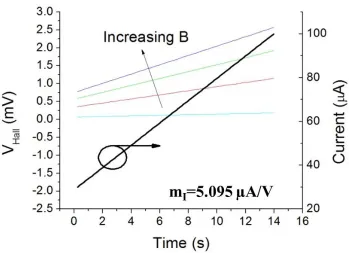
As a proof of concept, experimental results will be presented utilizing this proposed method of Hall effect characterization. Measured samples consist of square Hall effect structures on an AlGaN/GaN heterostructure with 100 µm Ti/Al/Ni/Au contacts. Contacts are labeled 1-4 as seen in figure 2.11. Current is applied between contacts 1 and 3 (I13) with a slope of mI=5.095 uA/s and Hall voltage (V24) is measured as a function of time. Current is applied using a Keithly 4200 SCS system by current ramping between 30 uA and 100 uA. Ramp rate mI can be altered by altering the measurement speed time constant in the Keithly 4200
Figure 2.14 Hall voltage measured as a function of time for a magnetic field increasing in increments. A linear dependence of VHall on time can be seen, as expected. The applied time
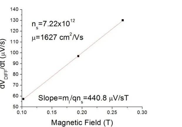
control software (KITE). Hall voltage is simultaneously measured using the Keithly 4200 system. Magnetic field was applied by placing the test sample on a flat, circular permanent magnet with an area much greater than that of the Hall test sample. Magnetic field was measured at the surface of the device under test with a gaussmeter. Following current application and voltage measurement, the magnetic field is increased by stacking another permanent magnet on top of the original magnet. This increases the magnetic field seen by the sample when placed on top of the magnet stack. Again, this magnetic field is measured by gaussmeter and current is applied and Hall voltage measured. A final magnetic field step was performed by adding another permanent magnet to the magnet stack for a total of 3 magnets. The measured Hall voltage for several steps of magnetic field is shown in figure 2.14. Taking the average slope of the Hall voltage over time curves allows for the
determination of as seen in Figure 2.15. The extracted sheet carrier density for these
samples is 7.22 x10¹² which is near the expected value of 8 x10¹² based on material parameters. The corresponding mobility value for this sample is 1627 cm2/Vs which
corresponds well with electrical measurements. Additionally, from figure 2.15 it can be seen that for this range of magnetic field a linear fit is a good approximation. This corresponds
with the assumption << further validating this procedure. This method allows for a
2.8 Physical characterization 2.8.1 Scanning Electron Microscopy
Scanning electron microscopy (SEM) allows for the magnification and imaging of features down to 15 nm and is a critical feature of electron beam lithography. The operating principle of SEM is that a beam of electrons is rastered in vacuum across the surface of the sample to be imaged. Electrons for the beam collide with the surface of the sample and transfer some portion of their energy to secondary electrons from the surface. If these secondary electrons have enough energy there are ejected from the sample being images and collected by a detector. The energy of these collected electrons is interpreted by the software as contrast and is then rastered to a computer monitor synched with the beam raster [33].
Features resolved with electron beam lithography can be as small as 10 nm and therefore SEM imaging is required for imaging critical electron beam lithography features.
Figure 2.15 Averaged slope of VHall for different magnetic fields. The slope of this plot corresponds to
Additionally, since electron beam lithography takes place in vacuum all visualization of the sample is done in real time using SEM. This is critical for alignment in electron beam lithography as SEM is used to find alignment marks and correlate the physical location of alignment marks with the programmed location of the alignment marks in the electron beam lithography mask.
2.8.2 X-ray Photoelectron Spectroscopy
X-ray photoelectron spectroscopy (XPS) is a powerful tool which allows the chemical composition and chemical interactions between materials to be analyzed. In the XPS measurement technique an X-ray source of a known energy is focused on the surface of the sample under test. The energy from the X-ray is transferred to the electrons in the sample resulting in the ejection of the electrons from the sample. These ejected electrons are collected utilizing a cylindrical mirror analyzer which extracts the number of electrons as a function of kinetic energy. The resulting spectrum of intensity as a function of kinetic energy allows for the extraction of numerous material parameters [34]. Many dielectrics presented in this work had not previously been deposited on GaN making XPS an extremely useful tool for determining dielectric and interface properties.
XPS analysis is performed ex situ using a Kratos Axis Ultra spectrometer equipped with a monochromatic Al Kα X-ray source (1486.6 eV) with a pass energy of 20 eV and a
referenced to the 285 eV peak of adventitious carbon to account for charging and calibration effects.
2.9 Simulation
Simulations were performed using Sentaurus TCAD simulator. The simulator solves finite difference equations at each point of a mesh representing the device under simulation. At each mesh point in the presented simulation data, Poisson and continuity equations for both holes and electrons were solved. To simplify simulations and aid in conversion several simplifications have been used.
(1) The two dimensional electron gas is represented as a continuous sheet charge at the AlGaN/GaN interface
(2) A GaN capping layer has not been included in the simulation
(3) There are no charges in the bulk of the gate dielectrics or at the dielectric interfaces
(4) There are no charges or traps in the bulk of the GaN or AlGaN
(5) Ohmic contacts are assumed and represented as highly doped AlGaN in contact with the 2DEG
room temperature all electrons reside in the conduction band of the metal-semiconductor which accurately represents the free electrons at the energy level of the work function of a metal.
3
PRELIMINARY GATE DIELECTRIC EVALUATION
3.1 Chapter Introduction
The choice of gate dielectric for a MOS-HFET will strongly affect device characteristics. Potential gate dielectric materials are characterized and evaluated in this chapter. The critical process steps developed for a GaN MOS-HFET process flow which enable dielectric evaluation are also presented.
3.2 Surface Cleaning
Gallium nitride will form a thin native oxide of mostly Ga2O3 [35] in air ambient which will impact the dielectric/GaN interface for a deposited dielectric. Therefore, before
Figure 3.1 Ga 2p3/2 spectra for the GaN surface before and after cleaning with NH4OH and HCl+HF chemistries. Both chemical treatments succeed in partially, but not
beginning characterization of dielectrics on GaN it is necessary to establish an appropriate surface cleaning method. Multiple surface cleaning techniques have been reported in literature with the most common chemical cleans consisting of NH4OH or HCl followed by HF chemistries [36]. To evaluate the efficacy of these cleaning chemistries GaN samples were prepared for characterization utilizing either a NH4OH or an HCl and HF clean.
Samples receiving the NH4OH clean were soaked in NH4OH for 1 min at room temperature. Samples with the acid clean were exposed to HCl:H2O 1:1 for 1 min followed by HF 1% for one minute. These samples, as well as samples in the as received (no clean) condition were then characterized by XPS. All samples were cleaned ex-situ and exposed to air ambient for approximately two hours prior to sample loading in the XPS chamber. It is expected that some native oxide growth will occur during this exposure to ambient. The Ga 2p3/2 spectra for each cleaning condition are shown in figure 3.1 for two incidence angles. The GaN substrate peak can be seen at 1117.5, which corresponds to Ga-N bonding [37]. The Ga-O peak at 118.4 separated 0.9 eV from the main peak corresponds to the Ga3+ bonding of Ga2O3 [38], [39]. The relative concentration of Ga-O and Ga-N bonding was fit using these peak positions, the 0.1 eV measurement error expected in these measurements may slightly alter fitted peak profiles. A reduction in the intensity of the Ga-O peak is observed for both NH4OH and HCl+HF cleans, however, neither cleaning method was able to completely remove the Ga-O peak [40]. It is expected that ex-situ measurement with exposure to
reported by Janzen et al. is saturated at approximately 0.79 monolayers at room temperature [41]. HCl+HF cleaning is seen to be slightly more effective at removing surface oxides than NH4OH as seen in the more surface resolved spectra at the incidence angle of 30°.
In order to further evaluate the surface clean, back to back capacitors were fabricated on HCl+HF cleaned GaN and untreated GaN. Capacitance voltage characteristics for these conditions with an 11 nm Al2O3 dielectric are seen in figure 3.2. In the case without cleaning the hysteresis is non-symmetric corresponding to a high interface state density. Following acid cleaning, the hysteresis becomes symmetric and reduces in magnitude. This symmetric behavior is an indicator of an improved GaN/Al2O3 interface with the observed hysteresis coming from bulk traps in the Al2O3. HCl+HF cleaning will therefore be used for inorganic surface cleaning before dielectric and metal depositions on the GaN surface.
3.3 Post Dielectric Annealing
is no increase in the concentration of Ga-O bonding with annealing temperatures up to 600 °C suggesting that the GaN/dielectric interface remains stable to at least 600 °C.
3.4 Preliminary Electrical Evaluation
Gate dielectrics Al2O3, HfAlO and SiO2 were selected for evaluation, deposited by ALD and evaluated using the back to back capacitor fabrication procedure. All dielectrics received a post deposition rapid thermal anneal at 600 °C for 60 s. HfAlO and ALD SiO2 were previously unexplored for GaN devices. Capacitance voltage profiles for the back to back capacitors with each dielectric are shown in figure 3.4. The dielectric constant of each dielectric is extracted from the accumulation capacitance of the 2DEG. As expected, HfAlO has the highest dielectric constant of k=13, with Al2O3 having k=8 and SiO2 with k=3.9.
Integrating the capacitance-voltage profile allows for the sheet charge concentration as well as the expected threshold voltage for a MOS-HFET device to be extrapolated [45]. The integrated capacitance voltage profile for each dielectric is shown in figure 3.5. The expected threshold voltage for the Al2O3 device is -4.3 V by linear extrapolation. HfAlO and SiO2 show threshold voltages of -3.7 V and -2.1 V respectively.
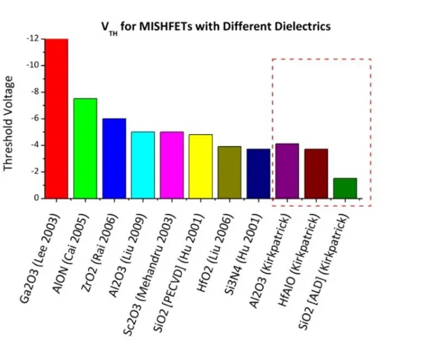
Figure 3.6 shows the threshold voltage of Al2O3, HfAlO and SiO2 in comparison to previously reported dielectrics. With enhancement mode operation in mind, ALD SiO2
Figure 3.4 100 kHz capacitance voltage profile for Al2O3, HfAlO and SiO2 back to back capacitors. Dielectric constant k is extracted from 2DEG accumulation capacitance
appears particularly attractive with a threshold voltage approximately 2 V closer to zero than other previously reported dielectrics (including SiO2 by PECVD). Threshold voltage
information as conveyed in figure 3.6 allows for a quick understanding of threshold voltage trends but has the potential to be misleading. Threshold voltage will decrease with increased gate dielectric thickness because of the increased gate/2DEG separation according to the relationship
(
) ( )
where VSchottky is the threshold voltage that would be obtained by forming the same gate stack without a gate dielectric. This voltage VSchottky is equivalent to the threshold voltage of a HFET device. As the capacitance of the gate dielectric increases either by decreasing dielectric thickness or by an increase in dielectric constant, the threshold voltage will move
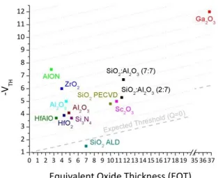
in the positive direction. Therefore to more accurately assess threshold voltage information, VT can be plotted as a function of EOT as seen in Figure 3.7. This representation normalizes dielectric constant allowing for dielectrics of the same EOT to be represented. Inserting the dielectric capacitance into equation 3.1 yields
(
) ( )
As seen in equation 3.2, threshold voltage linearly increases relative to EOT with a slope of
( ). The dashed line in figure 3.7 labeled “expected threshold voltage”
displays the line described in equation 3.2. For the dashed line, the gate stack is ideal without Figure 3.7 Threshold voltage as a function of EOT. Dotted and dashed lines are isocoulombic lines for increasing dielectric charge represented as fixed charge at the
any dielectric charge, interface charges or dipole effects. The dotted lines are isocoulombic lines of the same slope for cases of higher charge concentrations. Following these lines visually allows dielectrics of different EOT to be compared relative to one another where the perpendicular distance between the dielectric and a dashed line represents the level of charge in the gate stack. A lower charge concentration will thus lead to a more positive threshold voltage for the same EOT.
In both representations of threshold voltage, it can be seen that ALD SiO2 provides the most positive threshold voltage of any previously reported dielectric. Additionally, ALD of lower dielectric constant SiO2 warrants investigation with potential for lower-k passivation and reduced gate leakage due to the high band gap of SiO2. For this reason, ALD SiO2 was selected as a MOS-HFET gate dielectric for further evaluation.
3.5 Band Alignment of ALD SiO2, HfAlO, HfO2 and Al2O3
To further understand the physical properties of ALD dielectrics, the band alignment of the dielectric with GaN should be experimentally determined. The band gap and
band gap value [46], [47]. Dielectrics deposited by atomic layer deposition often have a smaller band gap than their bulk crystalline counterparts [48]as ALD dielectrics tend to be amorphous or nanocrystalline which changes the atomic ordering consequently effecting band gap. Al2O3 is a prime example of this with crystalline Al2O3 (sapphire) having a band gap of 8.8 while Al2O3 deposited by ALD shows a band gap ranging from 6.2-7 [13], [48]. Therefore, to accurately determine conduction band offset both valence band offset and band gap must be measured for the given dielectric/substrate. Utilizing XPS the band alignment of SiO2, HfO2, Al2O3 and HfAlO dielectrics deposited by ALD on GaN (0001) was determined. Valance band offset as well as band gap was measured in order to accurately determine conduction band offset.
for 60 s in N2 ambient. XPS measurements were performed ex-situ with samples exposed to air ambient for approximately 1 day following ALD deposition.
Figure 3.8 depicts the N 1s and Ga 3d core level spectra for the substrate following acid cleaning as well as for each dielectric as obtained by XPS. The peak at 397.6 eV in the N 1s spectra observed for clean GaN and GaN with SiO2 dielectric corresponds to N-Ga bonding from the GaN substrate [49]. However, a shift in the N core level peak position from 397.6 eV to 397.2 eV is observed for samples with Al2O3, HfO2 and HfAlO dielectrics. A similar cove level shift was observed from the Ga 3d core level spectra as shown in figure 3.8(b). The peak observed at 20.1 eV for clean GaN and GaN with SiO2 corresponds to Ga-N
Figure 3.8 N 1s and Ga 3d core level spectra for the GaN substrate following clean and for each dielectric. The shift in binding energy observed for HfO2, HfAlO and Al2O3
dielectrics corresponds to band bending at the GaN dielectric interface
bonding [49] whereas peak position for samples with Al2O3, HfO2 and HfAlO dielectrics are located at 19.7 eV. This shift in peak position of 0.4 eV seen in both N 1s and Ga 3d spectra is characteristic of band bending at the GaN dielectric interface. A shift to lower binding energy corresponds to upward band bending at the semiconductor dielectric interface [50]. The spontaneous and piezoelectric polarization of the GaN (0001) surface will result in bound negative charge at the surface. This charge will be screened by ionized donors
resulting in upward band bending [47], [50]. The GaN valance band maximum is referenced to the Fermi level at the surface of the sample. The measured GaN valance band maximum is therefore the difference between the GaN Fermi level and the energy of the surface of the sample inclusive of band bending .The photoelectron escape depth for this measurement is approximately ~2 nm with an expected band bending width of ~100 nm. The small escape depth length relative to the band bending width results in negligible variation in the measured surface energy due to band bending at the GaN surface [51].
Valence band offset measurements were performed according to Krauts method [51]. According to this method the energy separation between the substrate core level and the valence band edge is the same before and after dielectric deposition. Valence band offset can be calculated according to the following equation
(
) ( ) (
where Ga 3d is selected as the reference core level for the substrate. The reference selected for SiO2 is Si 2s due to its overlap in energy range with the Ga 3s peak. For HfO2 the reference is Hf 4f7/2 and for Al2O3 as well as HfAlO, Al 2p3/2 is used as the reference. XPS spectra for thin and thick dielectrics are shown in figure 3.9. The energy peak in figure 3.9(a) at 154.7 corresponds to Si-O bonding [52]. The peak in figure 3.9(b) at 16.9 corresponds to Hf-O bonding in the HfO2 dielectric [53]. The Al 2p spectra in figure 3.9(c) show a peak at 74.8 corresponding to Al2O3 bonding [54]. The Al 2p spectra for HfAlO with a peak at 74.4 are shown in figure 3.9(d). The shift in binding energy of the Al 2p3/2 peak seen in figure 3.9(d) corresponds to a laminate HfAlO rather than a layered HfO2, Al2O3 dielectric [13]. For all dielectrics it can be seen that the peak position for thin and thick dielectrics are identical.
Figure 3.9 XPS spectra for thin and thick dielectrics. Ga 3s (a) and 3d (b) peaks can be seen for samples with thin dielectrics
Therefore ( ) allowing equation 3.5 to be simplified as
( ) ( )
Valence band maximum (VBM) was found by linear extrapolation of the leading edge of the valence band spectra as illustrated in figure 3.10. The position of the VBM was determined to be 2.72 eV for the GaN sample following acid cleaning. VBM was measure as 5.08 eV for SiO2, 2.81 eV for HfO2, 3.56 eV for Al2O3 and 3.11 eV for HfAlO. Valence band offset at the GaN/dielectric interface was determined utilizing equation 3.4 to be 2.36 eV for SiO2,
Figure 3.10 Valence band spectra for clean substrate and each dielectric