ISSN (Online): 2319-8753 ISSN (Print) : 2347-6710
I
nternational
J
ournal of
I
nnovative
R
esearch in
S
cience,
E
ngineering and
T
echnology
(A High Impact Factor, Monthly, Peer Reviewed Journal) Visit: www.ijirset.com
Vol. 8, Issue 4, April 2019
Design and Analysis of Low Power
Application Based Median Filter Using Full
Adder Cell
N.Bhuvaneshwari
1,
P.Padmaloshani
2, Dr. G. Selvakumar
3Research Scholar, Department of Electronics and Communication Engineering, Muthayammal Engineering College, Tamilnadu, India1
Associate Professor, Department of Electronics and Communication Engineering, Muthayammal Engineering College, Tamilnadu, India2
Dean, Department of Electronics and Communication Engineering, Muthayammal Engineering College, Tamilnadu, India 3
ABSTRACT: In this system design and analysis of low power application based median filter using full adder is proposed. The Carry Save Array (CSA) multiplier is designed by using the proposed adder cell based on multiplexing logic. The median filter technique can be implement using this carry save array multiplier to remove the noises at low power and delay. Using complementary pass transistors logic (CPL) the area of full adder also reduced. The multiplier circuits are schematized and their layouts are generated by using Microwind software. Thus the full adder circuit based multiplier circuits gives better performance than other published results in terms of power dissipation and area due to less number of transistors used in adder circuit.
KEYWORDS: Structure of FIR Filter, Grouping flow for Canonic Signed Digit(CSD) Coefficients, Microwind MOS Layout, Carry Save Array (CSA) multiplier, Full adder cell, CPL .
I. INTRODUCTION
Low power design is necessary to extend the operating time of integrated circuits (ICs) as well as to reduce the packaging and cooling costs. As the scale of integration keeps growing, more and more complex signal processing systems are being implemented on a VLSI chip. These signal processing applications consume considerable amount of energy. The trade-off of performance and area remain to be the two major design factors, high power consumption is critical in today’s VLSI system design. The need for low power VLSI system arises from two main forces. First, Static power dissipation is due to the leakage current. Second, Dynamic power dissipation is due to the transition activity that dominates the total energy dissipation due to charging and discharging of capacitors. Multiplication is a fundamental operation in most signal processing algorithms. Multipliers have large area, long latency and consume considerable power. Therefore low-power multiplier design has been an important part in low- power VLSI system design.
ISSN (Online): 2319-8753 ISSN (Print) : 2347-6710
I
nternational
J
ournal of
I
nnovative
R
esearch in
S
cience,
E
ngineering and
T
echnology
(A High Impact Factor, Monthly, Peer Reviewed Journal) Visit: www.ijirset.com
Vol. 8, Issue 4, April 2019
II. RELATED WORK
Finite impulse response (FIR) filters are used in Digital Signal Processing applications. Accuracy in filter Designing is based on the Multiplication and accumulation of filter coefficients. Filters are digital filter whose response to the unit filter (Unit Sample Function) is finite in duration. This is in contrast to Infinite impulse response (IIR) filters whose response to unit impulse is infinite in duration FIR filter can be implemented using either recursive or non-recursive techniques, but usually non non-recursive technique are used. FIR filter is Finite IR filter and IIR filter is Infinite IR filter. FIR filters are non-recursive. The structure of FIR filter is shown in the figure 1.
Fig.2.1 Structure of FIR filter
Application Specific Integrated Circuits (ASIC) and field programmable gate arrays (FPGA) stages. Systolic plans speak to an appealing engineering worldview for effective equipment usage of calculation serious DSP applications, being upheld by the elements like effortlessness, consistency, and seclusion of the structure. Furthermore, they likewise have critical potential to yield high-throughput rate by abusing abnormal state of simultaneousness utilizing pipelining or parallel handling or both. In any case, the multipliers in these structures require a substantial bit of the chip-territory and thusly uphold impediment on the greatest conceivable number of processing elements (PEs) that can be suited and the most elevated request of the filter that can be figured it out. Multiplier less distributed arithmetic (DA)- based system, has increased considerable fame, lately, for their high-throughput handling capacity, and expanded consistency which brings about financially savvy and territory time productive processing structures.
III. EXISTING SYSTEM
In existing system, a novel RFIR filter design based on statistics centric reconfigurable (SCR) FIR filter architecture was designed.
A novel Canonic Signed Digit (CSD) coefficient grouping method is proposed simply by identifying whether there is only one single ”zero” bit between two ”non-zero” bits. Through analyzing distributions of the selected CSs among a large quantity of CSD coefficients taken from a widely representative the FIR filter designs, some statistical characteristics are observed and exploited.
A novel Processing Element (PE) structure for the medium-grain array architecture of reconfigurable FIR filters is proposed to achieve optimized utilization of logic resources for high performance.
The PE can be easily cascaded on a modular basis and is readily adopted for FPGA or application specified integrated circuit (ASIC) implementations.
ISSN (Online): 2319-8753 ISSN (Print) : 2347-6710
I
nternational
J
ournal of
I
nnovative
R
esearch in
S
cience,
E
ngineering and
T
echnology
(A High Impact Factor, Monthly, Peer Reviewed Journal) Visit: www.ijirset.com
Vol. 8, Issue 4, April 2019
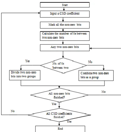
The grouping flow for Canonic Signed Digit (CSD) coefficients is shown in the below figure 3.1.
Figure 3.2, shows the architecture of a RFIR filter.The primary task of the pre-computer is to generate the partial products required by the coefficient multiplication. The partial products generated by the precomputer are then distributed to the cascaded array of Processing Element, and the coefficient multiplication is subsequently performed in the Processing Element, each performing shift and addition/subtraction operations.
Fig.3.1 Grouping flow for Canonic Signed Digit (CSD) coefficients
After selecting among the partial products generated from the pre-computer, a Processing Element accomplishes multiplication by performing required shifts and additions on those partial product.
ISSN (Online): 2319-8753 ISSN (Print) : 2347-6710
I
nternational
J
ournal of
I
nnovative
R
esearch in
S
cience,
E
ngineering and
T
echnology
(A High Impact Factor, Monthly, Peer Reviewed Journal) Visit: www.ijirset.com
Vol. 8, Issue 4, April 2019
But limitation of this method is that delay value is high because of decreased system speed and throughput. To overcome these problems, LC-CBA-RFIR method is introduced for evaluating ASIC implementation results and FPGA implementation results.
Low Cost Carry Bypass adder Reconfigurable Finite Impulse Response (LC-CBA-RFIR) is designed to perform the RFIR filter operations. In the CBA, Ripple Carry Adder (RCA) is employed to add four-bits at a time and the carry generated will be propagated to next stage with the help of multiplexer utilizing selected input as Bypass logic.
IV. PROPOSED SYSTEM
In the proposed system the multiplier is constructed by using adder cell. The CSA multiplier building block is containing half adder and full adder circuit.The proposed full adder circuit as shown in figure below combines the multiplexing operation for the sum operation and the carry operation. The sum and carry circuits are designed based on Standard full adder equations.
Full adder equation for SUM is SUM = C (A’B’ + AB) + C’(A’B + AB’)
Another form in which SUM can be implemented as SUM = C XOR ( A XOR B)
Full adder equation for CARRY is CARRY = AB + BC + AC
Another form in which CARRY can be implemented as CARRY = AB + C ( A EXOR B)
An input C and its complement are used as the control signal of the sum circuit. The two-input X-OR gate is developed using the multiplexer method. The output node of the two input multiplexer circuit is the differential node
According to standard full adder equation, the sum circuits need three inputs. In order to avoid increasing the number of transistors due to the addition of a third input, the following arrangement is made, the CPL(Complimentary Pass Transistor Logic ) XOR gate multiplying with C’s complement input and EX-NOR gate is multiplied with input C, and thereby reducing the number of transistors in the sum circuit.
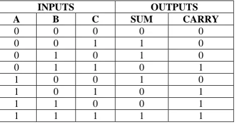
The truth table of full adder is given below
INPUTS OUTPUTS
A B C SUM CARRY
0 0 0 0 0 0 0 1 1 0 0 1 0 1 0 0 1 1 0 1 1 0 0 1 0 1 0 1 0 1 1 1 0 0 1 1 1 1 1 1
Table 4.1 Truth table of full adder
4.1.1 MULTIPLEXING LOGIC
ISSN (Online): 2319-8753 ISSN (Print) : 2347-6710
I
nternational
J
ournal of
I
nnovative
R
esearch in
S
cience,
E
ngineering and
T
echnology
(A High Impact Factor, Monthly, Peer Reviewed Journal) Visit: www.ijirset.com
Vol. 8, Issue 4, April 2019
operand size increases, linear arrays grow at a rate equal to the square of the operand size because the number of rows in the array is equal to the length of the multiplier, and the width of each row is equal to the width of multiplicand. The circuit diagram of the median filter using full adder cell is shown in the below figure 4.1.
Fig.4.1. Proposed Full Adder
The block diagram of sorting to find the median value of pixel is shown in the below figure 4.2.
ISSN (Online): 2319-8753 ISSN (Print) : 2347-6710
I
nternational
J
ournal of
I
nnovative
R
esearch in
S
cience,
E
ngineering and
T
echnology
(A High Impact Factor, Monthly, Peer Reviewed Journal) Visit: www.ijirset.com
Vol. 8, Issue 4, April 2019
4.1.2 ADVANTAGES OF PROPOSED SYSTEM
Low cost.
Less Area.
Low power and
High speed operation.
V.RESULT AND DISCUSSION
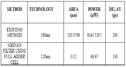
The Median filter using full adder cell was designed and analysed. The circit was simulated in microwind and their results were obtained. The comparision of area, power and delay for exisiting and proposed methods is presented in table 5.1.
Table 5.1 Performance Comparison of Exiting and Proposed method
In the multiplier array, a full adder with balanced carry and sum delays is desirable because the sum and carry signals are in the critical path. The speed and power of the full adder are very important for large arrays. Our proposed 1-bit adder cell consumes less power, and less area than the various proposed 1-bit adder cells, due to regular arrangement of transistor tree structure, less critical path and multiplexing method of designs. The only drawback of our proposed adder cell is that it occupies larger area. From the simulated results it is clear that the multiplier circuits designed based on the proposed adder cell gives better performance in terms of power, area than the CP L-based adder cell..
A. SIMULATION RESULTS
The simulation results by means of Microwind and DSCH tool. The microwind program allows to propose and simulating an integrated circuit at physical description level. MICROWIND is really integrated EDA software encompassing IC designs from concept to completion, enabling chip designers to design beyond their mind. MICROWIND integrates traditionally separated front-end and back-end chip design into an integrated flow, accelerating the design cycle and reduced design complexities.
ISSN (Online): 2319-8753 ISSN (Print) : 2347-6710
I
nternational
J
ournal of
I
nnovative
R
esearch in
S
cience,
E
ngineering and
T
echnology
(A High Impact Factor, Monthly, Peer Reviewed Journal) Visit: www.ijirset.com
Vol. 8, Issue 4, April 2019
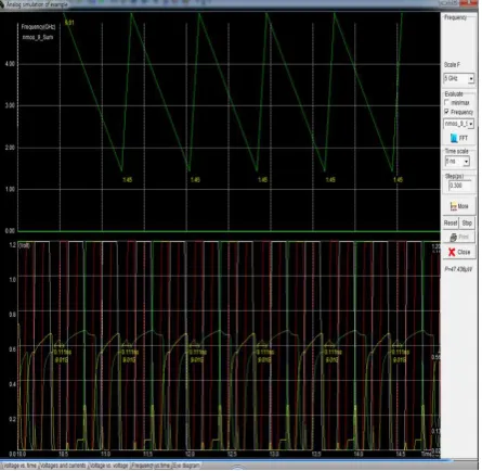
The microwind MOS layout is shown in the below figure 5.2. The simulation results are shown in below figures 5.3( Voltage vs Time),5.4 (Voltage vs Current ) 5.5 (Voltage vs Voltage), 5.6 (Frequency vs Time), 5.7( Eye diagram) respectively.
Fig.5.1 Schematic Design of proposed full adder
ISSN (Online): 2319-8753 ISSN (Print) : 2347-6710
I
nternational
J
ournal of
I
nnovative
R
esearch in
S
cience,
E
ngineering and
T
echnology
(A High Impact Factor, Monthly, Peer Reviewed Journal) Visit: www.ijirset.com
Vol. 8, Issue 4, April 2019
Fig.5.3 Simulation Waveform for Voltage Vs Time
ISSN (Online): 2319-8753 ISSN (Print) : 2347-6710
I
nternational
J
ournal of
I
nnovative
R
esearch in
S
cience,
E
ngineering and
T
echnology
(A High Impact Factor, Monthly, Peer Reviewed Journal) Visit: www.ijirset.com
Vol. 8, Issue 4, April 2019
Fig.5.5 Simulation Waveform for Voltage Vs Voltage
ISSN (Online): 2319-8753 ISSN (Print) : 2347-6710
I
nternational
J
ournal of
I
nnovative
R
esearch in
S
cience,
E
ngineering and
T
echnology
(A High Impact Factor, Monthly, Peer Reviewed Journal) Visit: www.ijirset.com
Vol. 8, Issue 4, April 2019
Fig 5.7 Eye Diagram
VI.CONCLUSION
The full adder based CSA(Carry Save Array) multipliers circuits are simulated by using Microwind software. The circuits were compared with existing circuits. The results were compared with existing resuts. The power and area wer reduced more than 50% than existing circuits and propogation delay also reduced. Thus Full adder based multiplier gives better performance than existing circuits in terms of power dissipation and area. The proposed multiplier circuits can be used in the low power application of VLSI circuits.
REFERENCES
[1] A. Bonetti, A. Teman, P. Flatresse, and A. Burg, “Multipliers-Driven Perturbation of Coefficients for Low-Power Operation in Reconfigurable FIR Filters”, IEEE Transactions on Circuits and Systems I: Regular Papers, Vol.64, No.9, pp. 2388 – 2400, 2017.
[2] J. Chen, J. Tan, C.H. Chang, and F. Feng, “A new cost-aware sensitivity-driven algorithm for the design of FIR filters”, IEEE Transactions on Circuits and Systems I: Regular Papers, Vol.64, No.6, pp.1588-1598, 2017.
[3] C.Y. Yao, W.C. Hsia, and Y.H. Ho, “Designing hardware-efficient fixed-point FIR filters in an expanding subexpression space”, IEEE Transactions on Circuits and Systems I: Regular Papers, Vol.61, No.1, pp.202-212, 2014.
[4] N. Bhagyalakshmi, K.R. Rekha, and K.R. Nataraj, “Design and implementation of DA-based reconfigurable FIR digital filter on FPGA”, In: Proc. of International Conf. on Emerging Research in Electronics, Computer Science and Technology (ICERECT), pp.214-217, 2015.
[5] A. Liacha, A.K. Oudjida, F. Ferguene, M. Bakiri, and M.L. Berrandjia, “Design of high-speed, low-power, and area-efficient FIR filters”, IET Circuits, Devices & Systems, Vol.12, No.1, pp.1-11, 2017.
[6] M. Alawad and M. Lin, “Fir filter based on stochastic computing with reconfigurable digital fabric”, In: Proc. of the International Conf. on Field-Programmable Custom Computing Machines (FCCM), pp.92-95, 2015.
[7] A. Rasekh and M.S. Bakhtiar, “Design of Low-Power Low-Area Tunable Active RC Filters”, IEEE Transactions on Circuits and Systems II: Express Briefs, Vol.65, No.1, pp.6-10, 2018.
[8] P.K. Meher and S.Y. Park, “High-throughput pipelined realization of adaptive FIR filter based on distributed arithmetic”, In: Proc. of the 19th International Conf. on VLSI and System-on-Chip (VLSI-SoC), pp.428-433, 2011.
[9] C.S.V. Patnam and E. Chitra, “Efficient FPGA Realization of DA-Based Reconfigurable FIR Digital Filter”, IJRECE, Vol.3, No.2, pp.24-28, 2015. [10] S. Bhattacharjee, S. Sil, and A. Chakrabarti, “Evaluation of Power Efficient FIR Filter for FPGA based DSP Applications”, Procedia Technology, Vol.10, pp.856-865, 2013.
[11] J.L.M. Iqbal and S. Varadarajan, “High Performance Reconfigurable FIR Filter Architecture Using Optimized Multiplier”, Circuits, Systems, and Signal Processing, Vol.32, No.2, pp.663-682, 2013.
[12] R. Thakur and K. Khare, “High Speed FPGA Implementation of FIR Filter for DSP Applications”, International Journal of Modeling and Optimization, Vol.3, No.1, pp.92, 2013.
[13] S.J. Lee, J.W. Choi, S.W. Kim, and J. Park, “A reconfigurable FIR filter architecture to trade off filter performance for dynamic power consumption”, IEEE transactions on very large scale integration (VLSI) systems, Vol.19, No.12, pp.2221-2228, 2011.