Design, Fabrication and Implementation of
Microcontroller Controlled Static Var Compensator
G.PREMKUMAR
AMRITA SCHOOL OF ENGINEERING AMRITA UNIVERSITY
B.MUTHUKUMAR
AMRITA SCHOOL OF ENGINEERING AMRITA UNIVERSITY
ABSTRACT
Power factor correction is vital in present society. The two key benefits of power factor correction, which includes reduced power costs and higher system capacity. Implementation of Flexible AC Transmission Systems (FACTS) improves the power factor, power transfer capability and voltage stability. The shunt type of FACTS controller is used to either absorb or inject VARs into the system, thereby compensating reactive power. The design, fabrication and testing of microcontroller controlled Static VAR Compensator (SVC) consisting of Thyristor Controlled reactor (TCR) and Thyristor Switched Capacitor (TSC) are dealt with in this paper. A microcontroller is used to calculate the load displacement power factor (DPF) and for executing the fuzzy logic control scheme for TCR branch. The details of the design, fabrication, test results of Thyristor Controlled Reactor and Thyristor Switched Capacitor and their capability to improve their power factor performance are the main aim of this paper.
General Terms
Microcontroller controlled Static Var Compensator, Thyristor Controlled reactor (TCR), and Thyristor Switched Capacitor (TSC).
Keywords
Displacement power factor, Firing angle, Fuzzy logic, Harmonics, Reactive load, microcontroller, Residential load, Static var compensator, Triac, True power Factor.
1.
INTRODUCTION
As the demand for electric power grows the energy efficiency term is very significant. Electric load consuming alternating currents consume both active power and reactive power. The active power does useful work and reactive power dissipates no energy in the load and return to the source on current cycle. When the inductive loads are connected to the power system network, the voltage at the consumer side reduces due to high reactive power requirement. This is due to the increased load current caused by increased reactive power consumption due to the lagging power factor of the inductive load. This will increase the system losses and hence reduces the efficiency. A conventional method for mitigation is problem is to use capacitors for supplying the required reactive power. Use of a set of capacitors may be significant to compensate the lagging power factor for an inductive load.
In a real time scenario, the load will change continuously and
power electronics in which SVC is very simple and common method for reactive power compensation.
[image:1.595.367.501.245.367.2]
Fig. 1. Typical SVC Configuration with TSC and TCR Branches [1].
The focus of this project has been on a particular FACTS (Flexible AC Transmission System) device – the Static Var Compensator (SVC) as shown in Fig 1. The SVC is a proven technology for power factor correction and reactive power compensation. Traditionally, the SVC has been used as a shunt-connected device that offers voltage stability and load compensation to the power system at particular points such as transmission line 4midpoints or near varying loads. Since EPRI’s (Electric Power Research Institute) release of the FACTs strategies in 1987, SVC’s have grown in popularity and are well regarded in the power industry [1].
The SVC comprise capacitor bank controlled by triac called Thyrsitor Switched capacitor (TSC) and reactor bank controlled by triac called Thyristor controlled reactor (TCR). These compensators draw reactive power from the line there by regulating voltage, improving stability, control overvoltage and reduce voltage flicker. Since static Var compensators use switching for reactive power control, these are also called static VAr (Reactive power) switches or systems.
2.
HARDWARE DESIGN
2.1 POWER FACTOR MEASUREMENT [11]
The power factor of an AC electric power system is defined as the ratio of the real power to the apparent power, and is a number ranging between 0 to 1 inclusive. Real power is the capacity the circuit performance in a given time. Apparent power equals to the product of the current and voltage of the circuit used. Energy when stored in the load and returned to the source or due to a non-linear load that distorts the wave of the current drawn from the source, the apparent power equals to or greater than the real power. Low power factor increases losses in a power distribution system and thus resulting in increased cost for electrical energy use.
In purely resistive AC circuit, voltage and current waveforms are in step, changing the polarity in every cycle. In circuits having reactive loads, containing capacitors or inductors, the energy is stored and hence resulting in a difference between voltage and current waveforms. The stored is not used for load as it returns to source. When a circuit has a low power factor it has higher currents to transfer at a given quantity of power than a circuit having higher power factor.
Circuits containing only heating elements like filament lamps, strip heaters and cooking stoves etc. have a power factor of unity. Circuits containing inductive or capacitive elements such as lamp ballasts and motors etc. often have a power factor below 1.0. The significance of power factor lies in the fact that utility companies supplies customers with volt-amperes, but in real they bill them for watts. The circuits having power factors less than unity require a utility to generate more than the minimum volt-amperes necessary to supply the real power (watts). This increases generation and transmission costs. Good power factor is which is greater than 0.85 or 85%. Utilities may charge additional costs to customers who have a power factor below some limit.
A power factor of 1 or "unity power factor" is the goal of any electric utility company since if the power factor is below 1, it has to supply more current to the user for a given amount of power usage. In doing so, they have more line losses. They should have larger capacity equipment in place than would be necessary. Resulting in the industrial facility to be charged a penalty if its power factor is much varying from unity. Industrial facilities mostly have lagging power factor, where the current lags voltage as in inductor. This primarily results having a lot of electric induction motors - the windings of motors act as inductors as seen by power supply. Capacitors have opposite effect and can compensate the inductive windings. A very few industrial sites have large banks of capacitors strictly for the purpose of correcting the power factor back toward one to save on utility company charges.
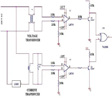
Fig 2: Power factor measurement circuit
From the shown Fig 2, the voltage transducer is used to step down the mains supply voltage to low voltage level. The voltage level is from 230V AC to 6V AC. Then the output of the voltage transducer is given to Zero Crossing Detector. The current consumed by the load is measured with the help of a current transducer. The current transducer will convert the load current in to lower values that current output will be converted in to voltage with the help of the shunt resistor. Then the corresponding the AC voltage is given to zero crossing detector. The Zero Crossing Detector is used to convert the sine wave to square wave signal.
[image:2.595.327.545.77.267.2]The zero crossing detectors are constructed by the operational amplifier LM 741. The inverting and non-inverting input terminals are connected to the potential transformer and current transformer terminals respectively. So the input sine wave signal is converted in to square wave signals. The square signal is in the range of +12v to -12v level. Then the square wave signal is given to base of the BC 547 switching transistor in order to convert the TTL voltage 0 to 5v level. Then the both ZCD’s outputs as in Fig 4 shown are given to logical XOR gate 74LS86 to find the phase angle difference between the voltage and current. The XOR gate output is given to microcontroller or PC and calculates the power factor with help of software.
Fig 4: XOR gate Input
2.4 VOLTAGE TRANSDUCER CIRCUIT
LEM LV-20 P voltage transducers have been used to sense inverter output voltage and grid voltage. A current proportional to measured voltage is passed through external resistor. This resistor has been installed in series with the primary circuit of the transducer. Transducer’s optimum accuracy is obtained at the nominal primary current, +15V and -15V.
Voltage to be measured = 230V
Let the input resistance be 33KΩ
Then the input current for 33KΩ = 230/33KΩ = 6.9mA
Conversion ratio = 2500:1000
Secondary rms current = 6.9*2.5 = 17.25mA
Since the secondary voltage can be maximum of only 2.5v,
Measuring resistance = 2.5/17.25mA = 144.92Ω The chosen value of secondary resistance 100Ω
2.5 CURRENT TRANSDUCER CIRCUIT
The load current is to be sensed and is given as the input to the microcontroller. LEM module LA 25-NP current transducer is used to sense the load current. The turns ratio selected is 3/1000. The recommended measuring resistance range is from 100 ohm to 320 ohm.
Peak load current = 10A
Secondary voltage should be less than 2.5V, Conversion ratio is 3/1000.
Secondary resistance R= (2.5*(1000/3))/10) =83.3Ω Hence the secondary resistance chosen is 100 Ω.
2.5 LEVEL SHIFTER
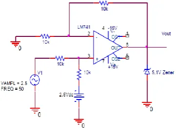
[image:3.595.333.514.251.387.2]The ADC module of PIC 16F877A accepts only positive voltages and a maximum of 5V is possible since the maximum reference voltage to the ADC module is 5V. So the load voltage and load current sensed by the PT and CT is shifted by 2.5V DC. The reason for shifting by 2.5V is because, the maximum peak positive voltage of the PT and CT is 2.5V and maximum peak negative voltage is -2.5V. So when shifter by 2.5V DC, we get an output voltage in the range 0 to 5V, which is needed for the ADC module of the PIC 16F877A. The level shifting is done using op-amp adder configuration in non-inverting mode with one input from the CT and the other is 2.5V DC. The output is limited to 5.1V using a zener diode at the output. The circuit diagram of level shifter is shown in Figure 6.
Fig 6 : Level shifter circuit
2.6 LCD DISPLAY
A LCD of 2x16 ASCII-text is installed on a PCB board, having 4 data and 3 command pins as input/output. A 5V DC supply is given to the LCD.A 10K pot is used to adjust the contrast in the display. This LCD application is used to display the load voltage, load current, power factor and the capacitor value which is need to compensate the lagging reactive power.
2.7 DC POWER SUPPLY
[image:3.595.95.296.544.727.2]Fig 7: DC power supply circuit
2.8
TSC AND TCR BRANCH DESIGN
2.8.1
Thyristor Controlled Reactor (tcr):
A shunt-connected inductor with effective reactance is varied in a continuous manner by partial-conduction control of the thyristor valve, TCR (shown in Fig 8) is a subset of SVC in which conduction time and hence, current in a shunt reactor is controlled by a thyristor-based ac switch with firing angle control.
Fig 8: Circuit diagram of TCR
The controlling element in TCR is the thyristor controller, shown above are a pair of anti-parallel thyristors which conduct during alternate half cycles of the supply voltage. If the thyristors are gated into conduction precisely at the peaks of supply voltage, when fully conducted resulting in the reactor, and the current is same as though the thyristor controller were short-circuited. The current is essentially reactive, lagging behind the voltage by nearly 90o. It contains a small in-phase component due to power loss in the reactor, which may be of the order of 0.5-2% of the reactive power.
Each of these corresponds to a certain value α, the gating angle measured from a zero crossing of voltage. Full conduction is obtained with gating angle of 90o. Partial conduction is obtained with gating angles between 90o and 180o.
The effect of increasing the gating angle is to reduce the fundamental harmonic component in the current. Equivalent to an increase in the inductance in the reactor, reducing the reactive power and its current. So far as the fundamental component of current is concerned, the thyristor-controlled reactor is controllable susceptance,and therefore is applied as a static compensator.
2.8.2
THYRISTOR SWITCHED CAPACITOR (TSC): [image:4.595.359.478.194.292.2]A shunt connected capacitor whose effective reactance is varied in a stepwise manner by full or zero conduction operation of the thyristor valve, TSC (shown in Fig 9) is also a subset of SVC in which thyristor based ac switches are used to switch in and out (without firing angle control) shunt capacitor branches, which will achieve the required step change in the reactive power supplied to the system. Unlike shunt reactors, shunt capacitors cannot be switched continuously with variable firing angle control.
Fig 9: Circuit diagram of TSC
2.9
Microcontroller and SVC Branch (TSC
And TCR) Interfacing:
The microcontroller controls the TCR and TSC branches by giving the control signal to a triac driver which is called optocoupler. An optocoupler is essential to control each individual branch utilized. For example, if a bank of 9 capacitors (TSC) are used and 1 inductor (TCR), then 10 triac drivers will be needed. Likewise, each branch must be given a dedicated port on the microcontroller. The need of the optocoupler (MOC3011) is to isolate the high voltage triac from lower voltage control. This electrical isolation helps to ensure that the microprocessor remains isolated from the high voltage as shown in Fig 10. Since the MOC3011 is a current activated device, the proper resistor to be placed between the MOC3011 and the microprocessor must be chosen correctly. In this example, two output microcontroller ports were utilized to drive the two triac drivers [1].
Fig 10: Interface between the Microcontroller and Optocoupler
2.9.1
TRIAC SELECTION [image:4.595.104.213.388.475.2] [image:4.595.319.515.515.606.2]2.9.2
DRIVER CIRCUIT DESIGNFig 11: Triac Switching Circuit
In the shown Fig 11 the on/off pulses are given from the microcontroller to transistor BC557. This transistor will conduct only if the pulses received from the microcontroller if it the pulses are received then the signal are given to the BC547 which acts as a switch and then the pulses are given to the optocoupler in which the led blinks so that the phototransistor conducts. Due to this the signal, is transferred to the triac gate so mt1 and mt2 terminal gets shorted so that we get constant output voltage such as 230V in the load. The threshold gate voltage for the triac is 1.5V.
3.
SOFTWARE DESIGN
[1]3.1
Microcontroller Software Design and
Implementation
The PIC microcontroller is responsible for Power Factor calculation through zero crossing detection, TSC switching control, fuzzy control of the TCR branch and LCD output.
3.1.1
Power Factor Calculation:
The displacement power factor , which is indirectly the control input for both the TSC and TCR branches, is calculated by having the microprocessor determine the time difference between the reactive load’s voltage and current waveforms. The following list summarizes the functional and mathematical steps taken by the microprocessor to calculate the displacement power factor. The list will be expanded into subsections to provide specific microprocessor implementation details.
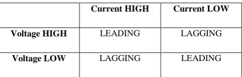
1. Determine Whether the Reactive Load is Leading or Lagging
2. Calculate the Time Difference Between Voltage and Current Waveforms
3. Convert the Time Difference to a Phase Angle Difference
4. Convert Phase Angle Difference to PF
D
[image:5.595.53.276.80.217.2]voltage waveform and then immediately record the state of the current waveform. By comparing the waveform states, the PIC can determine whether the current is leading or lagging the voltage. To detect a zero crossing, the PIC continuously polls a waveform watching for its value to flip. For example, if the PIC read a HIGH for the voltage, then a loop continuously polling the voltage would detect when the voltage input flipped to a LOW. When that occurs, the PIC has detected a zero crossing. If the voltage waveform was recorded as HIGH after the zero crossing, and the current waveform was recorded as LOW, then it is determined that the current is lagging the voltage. Likewise, if the voltage was recorded as HIGH, and the current was already HIGH, then the current would be considered leading the voltage. Because a voltage zero crossing is needed for synchronization, the PIC needs half a cycle to determine whether the current waveform is leading or lagging. Table 3.1 shows all of the possible combinations of the current waveform leading or lagging logic. Note that the voltage waveform is the first waveform to be polled after the zero-crossing is detected.
Table 12: Logic to find whether current is Lagging/Leading Voltage [1]
Current HIGH Current LOW
Voltage HIGH LEADING LAGGING
Voltage LOW LAGGING LEADING
3.1.3
Calculating the Time Difference (ΔT) BetweenVoltage and Current Waveforms
Once it has been determined whether the current is leading or lagging the voltage, the PIC will calculate the time difference separating the two waveforms. If the current is lagging the voltage, the PIC will wait for the voltage to cross zero at the next half cycle and then start its 16-bit timer. The PIC will then wait for the current to cross zero. Once the current crosses zero, the timer is stopped and its value is stored in a variable. Likewise, if the current is leading the voltage, the PIC will wait for the current to cross zero at the next half cycle and then start its 16-bit timer. The PIC will then wait for the voltage to cross zero, and when this occurs, the PIC will stop its timer and record the value to a variable. Calculating this time difference takes one half cycle because the waveform zero crossings are needed to synchronize the timer.
3.1.4
Converting the Time Difference (ΔT) to a
Phase Angle Difference (θ)
[image:5.595.312.553.309.386.2]3.1.5
Converting the Phase Angle Difference (θ)
to Displacement Power Factor
The Displacement Power Factor (DPF) can be calculated easily by taking the COSINE of θ. By performing this calculation is optional for the PIC because, θ is used as the control variable for the TSC and TCR branches. If a slower clock frequency was chosen this calculation could be omitted to save processing time.
3.2
TSC Switching Control [1]
The optimum capacitor configuration for the individual TSC branches can be found by sizing the capacitors in binary steps. For the SVC prototype, the binary steps of 1uF, 2uF, 4uF, 8uF, 16uF, 32uF and 64uF were chosen to provide a total of 128uF in discrete steps of 1uF with only using 7 capacitors. This flexibility allows for a tightly configured displacement power factor compensation that can be easily programmed to be either leading or lagging. as shown in Fig 12 illustrates the TSC branches configured in binary steps.
The binary configuration is important to the software design because the PIC must be able to intelligently switch in and out the appropriate TSC branch at the appropriate time. Every 5 seconds the PIC is programmed to examine the current phase angle difference (θ) and switch in or out the next capacitor size in binary order. Generally, if θ positive (lagging Displacement Power Factor (DPF)) the PIC will switch in TSC branches in binary order (increments of 1uF) until θ is no greater than –20° (leading DPF). Likewise, if θ is negative (leading DPF) the PIC will switch out TSC branches until θ is approximately –20° (leading DPF).
This overcompensation leading by approximately 20° is needed so the TCR branch can fine-tune the DPFto a value closer to unity.
As presented earlier, the only time the TSC branch should be switched is during the zero crossing of the current so transients are avoided. The PIC is programmed is examine θ every 5 seconds, but this time value is arbitrary and should be configured to best match the specific application. It is recommended that a time value not less than 5 seconds be used so that the PIC is not continuously updating the TSC branches. When the time interval expires the PIC will wait for the next current zero crossing.
[image:6.595.319.559.78.245.2]This is accomplished by having the PIC poll the current waveform input looking for a state change. For example, if the current waveform is initially read as HIGH, then when the waveform switches to a LOW, a zero crossing has occurred. Having already made its TSC switching decision based upon θ, the PIC will either switch in or out a single TSC branch at this exact instant. Fig. 13 summarizes the steps taken by the PIC during TSC branch switching.
Fig 12 TSC Branches Configured in Binary Steps [1]
Fig 13 : Steps for switch in and out TSC branch. [1]
3.3
TCR Fuzzy Logic Control Strategy
[image:6.595.338.550.286.489.2]Fig 14: Steps for controlling the TCR branch [1]
3.4
Software Implementation
The software for the PIC was developed using the C programming language and a specific PIC C compiler, known as “PICC”, which is distributed by CCSInfo [5]. This compiler compiles the C source code and generates the equivalent assembly instructions. A software PIC programmer known as MPLAB, distributed by Microchip, was chosen as the tool that would program the PIC microcontroller once the assembly code had been generated [6]. MPLAB transfers the microcontroller instructions from the PC to the PIC via a serial cable. Once the PIC has been programmed, the PC, serial cable, and developer software is no longer needed. The PIC is capable of executing completely autonomously. Fig. 15 summarizes the functionality of the microcontroller.
Fig 15 : Functional Block Diagram of Microcontroller [1]
4.
IMPLEMENTATION
OF
CONTROL
[image:7.595.100.226.70.301.2]CIRCUIT FOR TSC AND TCR BRANCH
[image:7.595.317.545.274.478.2]Fig 16: Control circuit for SVC (TSC –TCR)
Fig 17 : Binary ratios of capacitor bank ( TSC) and TCR
5.
CONCLUSION
In this paper, microcontroller controlled SVC is designed, fabricated, tested manually and controlled automatically to get unity power factor by supplying variable reactive power to the system shown in Fig 15, Fig 16. The hardware and software of this SVC control system is developed based on Microcontroller PIC 16f877A chip, one of the low cost industrial controller. The power circuit of single phase 2KVAR TSC-TCR type SVC have been design and tested experimentally using a test system.
The future scope of this project is to design filter to reduce the harmonics in the system, control the SVC through LABVIEW and the values like voltage, current, power factor and reactive power can transmit wirelessly through ZIG-BEE or using ARDUINO.
6.
REFERENCES
[image:7.595.58.293.485.615.2]Compensator to Enhance Power System Stability”, IEEE Transactions on Power Systems, Vol. 14, No. 1, Feb. 1999 pp. 186-191
[3] A. Gelen, T. Yalcinoz. “Simulation of TSC on voltage regulation for static and dynamic load models using MATLAB.in Proc. of the IEEE 38th North American Power Symposium (NAPS), Illinois, USA, September 17-19, 2006.
[4] N. G. Hingorani, L. Gyugyi. Understanding FACTS: Concepts and Technology Flexible AC Transmission Systems. New York: IEEE Press, 1999.
[5] R. M. Mathur, R. K. Varma. Thyristor-Based FACTS Controllers for Electrical Transmission Systems. New York:IEEE Press, 2002.
[6] B. Endres, G. Thiele, I. Bonfanti, G. Testi. “Design and operational testing on thyristor modules for the SVC Kemps Creek.” IEEE Trans. on Power Delivery, pp. 1321-1326, November 1989.
[7] P. Mehta, M. Darwish. “Active reactive-power controller.” in Proc. IEE Electric Power Applications, Vol. 142, Issue.6, pp. 405-409, November 1995.
[8] Q. Gu, A. Pandey, S. K. Starrett. “Fuzzy logic control schemes for static var compensator to control system damping using global signal.” Electrical Power System Research, Vol. 67, Issue. 2, pp. 115-122, November 2003.
[9] T. Ahmed, K. Nishida, K. Soushin, M. Nakaoka. “Static var compensator-based voltage control implementation of single-phase self-excited induction generator.” IEE Proc. Generation Transmission & Distribution, Vol. 152, Issue. 2, pp. 145-156, March 2005.
![Fig. 1. Typical SVC Configuration with TSC and TCR Branches [1].](https://thumb-us.123doks.com/thumbv2/123dok_us/8062823.776950/1.595.367.501.245.367/fig-typical-svc-configuration-tsc-tcr-branches.webp)

![Fig 12 TSC Branches Configured in Binary Steps [1]](https://thumb-us.123doks.com/thumbv2/123dok_us/8062823.776950/6.595.338.550.286.489/fig-tsc-branches-configured-binary-steps.webp)
![Fig 14: Steps for controlling the TCR branch [1]](https://thumb-us.123doks.com/thumbv2/123dok_us/8062823.776950/7.595.100.226.70.301/fig-steps-controlling-tcr-branch.webp)
