How to cite this paper: Hussain, K.M.A., Faruqe, T. and Sullivan, J.L. (2014) Characteristics of Diamond-Like Carbon Thin Film Semiconductor for Photovoltaic Application. Open Access Library Journal, 1: e616.
http://dx.doi.org/10.4236/oalib.1100616
Characteristics of Diamond-Like Carbon
Thin Film Semiconductor for
Photovoltaic Application
K. M. A. Hussain
1, T. Faruqe
1, J. L. Sullivan
21Experimental Physics Division, Atomic Energy Centre, Dhaka, Bangladesh
2Surface Science Research Group, Electronic Engineering, Aston University, Birmingham, UK
Email: [email protected]
Received 5 May 2014; revised 15 June 2014; accepted 20 July 2014
Copyright © 2014 by authors and OALib.
This work is licensed under the Creative Commons Attribution International License (CC BY).
http://creativecommons.org/licenses/by/4.0/
Abstract
Diamond-Like Carbon (DLC) thin film semiconductors were produced by Radio Frequency Plasma Enhanced Chemical Vapour Deposition (RF-PECVD) method and characterized by nanoindentation to investigate its mechanical properties for protective coating applications. The XRD analysis showed that the films were hydrogenated amorphous carbon (a-C:H) nature. The thickness of the films was measured by Ellipsometry and Profilometry. The thickness variation with deposition rate followed a linear relationship within the various deposition parameters showed a good ho- mogeneity formed of DLC films. The hardness value linearly varied with RF power at 30 mTorr showed an optimum pressure to form a quality DLC thin film. The optimum RF power and CM pressure was 150 watt and 30 mTorr showed the thin film hardness 18.73 ± 2.51 GPa and reduced modulus 171.04 ± 11.13 GPa and the films were investigated as hard hydrogenated amorphous carbon (a-C:H) structure. The high hardness value and the deposition parameters showed that the deposition method of RF-PECVD was a controlled deposition process especially for a-C:H DLC thin film deposition. The thickness effects on hardness of the film implied that the optimum deposition condition was an important aspect to get quality DLC films for protective coating application.
Keywords
Diamond-Like Carbon, Nano-Indentation, X-Ray Photoelectron Spectroscopy
Subject Areas: Applied Physics, Experimental Physics
1. Introduction
OALibJ | DOI:10.4236/oalib.1100616 2 July 2014 | Volume 1 | e616
chanical hardness, chemical inertness, optical transparency and its wide band gap properties showed widespread applications as protective coatings, antireflective and protective encapsulates for photovoltaic (PV) and elec- tronic application [1]. The DLC films were produced by different types of chemical and physical vapour deposi- tion (CVD and PVD) method such as chemical vapour deposition [2], filtered cathodic vacuum arc [3], micro- wave plasma-assisted deposition [4], mass-selected ion beam deposition [5], and pulsed laser deposition [6]. It was possible to obtain high quality DLC films at rapid growth rates but it was more difficult and costly to depo- sit DLC films on a large area substrate using these methods due to the complicated equipment and rigorous preparation conditions. The RF-PECVD method is widely used for synthesis of DLC films due to standard plasma processing technology which could allow the simple and relatively inexpensive low temperature coating on a large area and uniform coating of substrates having different shapes and sizes [7]. The hardness and Young’s modulus of the films are important to investigate for protective application. In this study, the DLC thin films were deposited on silicon substrates using RF-PECVD method by varying RF power and working pressure at constant methane: hydrogen composition ratio 3:1 and deposition time. The structural and mechanical proper- ties were analyzed to optimize RF power and working pressure for producing a quality DLC thin film for pro- tective application.
2. Experimental
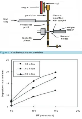
Diamond-like-carbon (DLC) thin films are produced on silicon substrates by RF-PECVD method. The plasma system of RF-PECVD method reported in detail in the paper [7] [8]. The system used in the RF-PECVD method includes an optional quartz plate approximately 12 mm thick on which the sample was placed. Quartz was cho- sen because it did not readily increased contamination in the chamber through plasma processing and for incor- rectly placed in the middle of the electrode, it would not interfere with the creation of the plasma by shorting out between the electrode and the dark space shield. The experiments performed consisted of a matrix defined by the parameters, working pressure, rf power and percentage of methane in hydrogen. The total gas flow remained fixed at 20 sccm between methane and hydrogen ratio 3:1. The RF power was varied from 50 to 150 watt and the working pressure was varied from 30 mTorr to 90 mTorr. The deposition time was fixed at 15 minutes. The structure of the film was characterized by XRD analysis. The mechanical properties of DLC thin films were measured by nano-indenter. Nanoindentation was employed to evaluate hardness and Young’s modulus of the films. The thickness of the films was performed by the Ellipsometry and Profilometry analysis. The surface roughness, topography and morphology were estimated from AFM analysis. XRD was used to characterize the films structural properties. In XPS, the sample is illuminated with X-rays which excite photoelectron from the surface. The photoelectron energy is dependent on the precise chemical configuration of the surface atom and pronounced chemical shifts are produced in the position of the peaks in the XPS spectrum. The chemical infor- mation obtained from the chemical shifts in the photoelectron energies. In the nanoindentation method, a Nano Test System was used manufactured by Micro Materials, Wrexham, UK. The heart of the Nano test is a pendu- lum based depth-sensing system shown inFigure 1. The sample mounted vertically and the load applied elec- tromagnetically. DC current from coil causes the pendulum to rotate on its frictionless pivot such that the dia- mond probe penetrates the film surface. Test probe displacement is measured with the parallel plate capacitor with sub-nm resolution. The diamond indenter (Berkovich-three sided pyramidal) was used for all the indenta- tion testing. The measured depth is adjusted for the effect of instrument compliance in the instrument software. The indentation loading and unloading was set equal in all the tests. Fused quartz was used as a calibration standard recognized by the nanoindentation standard because its hardness and elastic modulus do not very sig- nificantly with indentation depth. The area function of the indenter was determined with the calibration experi- ment to obtain meaningful values of hardness and elastic modulus. Indentations were load controlled and re- peated 8 to 12 times on different regions of the film surface. In this analysis, no sample preparation was required and the analysis was performed quickly and inexpensively.
3. Results and Discussion
OALibJ | DOI:10.4236/oalib.1100616 3 July 2014 | Volume 1 | e616 Figure 1. Nanoindentation test pendulum.
Figure 2. Deposition rate and pressure varied with RF power.
pressure in the experimental conditions because the increase of RF power (50 to 150 watt) enhanced the plasma density results the deposition rate increased.
[image:3.595.172.459.82.500.2]The deposition rate was 8 nm/min, 16 nm/min and 19.67 nm/min for the variation of RF power 50 watt, 100 watt and 150 watt respectively at 90 mTorr. Similar characteristics of deposition rate were found at 30 mTorr and 60 mTorr. The three lines were not linear in Figure 2 because the deposition rate was not comparatively in- creased [9] at 150 watt due to enlarge plasma sheath region. The analysis showed that the plasma diagnostic was controlled by the RF power and working pressure. The analysis showed that the 30 mTorr and 150 watt (data in
OALibJ | DOI:10.4236/oalib.1100616 4 July 2014 | Volume 1 | e616
spectrum, thickness of the film was measured. The analysis showed that the plasma diagnostic tool was con- trolled with thickness and the controlled deposition rate showed to form quality DLC thin films. The deposition time was 15 minutes.
The nanoindentation test demonstrates the hardness and reduced modulus of the films are presented in Figure 4
and Figure 5 respectively. The hardness was varied with RF power and working pressure and the Figure 4
showed that the maximum hardness was 18.73 ± 2.51 GPa and the respective reduced modulus inFigure 5 was 171.04 ± 11.13 GPa at 150 watt and 30 mTorr. The result was collected from the following nanoindentation spectrum is presented inFigure 6.
The nanoindentation load and depth is presented in the followingTable 1.
The table shows that the penetration depth is less than 10% of the measured thickness. The result showed that the nanoindentation of the films was successfully performed and the films are diamond-like carbon structure and the results were in good agreement with the reported values [11] [12]. The high power 150 watt was expected optimum because the film toughness decreases with the film thickness due to the limited crack [13].
The analysis showed that the formation of hard DLC was form at minimum pressure 30 mTorr and at maxi- mum rf power 150 watt. The result showed that the hardness was controlled at 30 mTorr for varied RF power and the high hardness was at 150 watt.
The surface layer of the film was identified by XRD analysis shown in Figure 7 using X-ray Diffraction. The spectrum showed that the DLC films are amorphous characteristics. The analysis was identical suggested by the
Figure 3. Deposition rate varied with thickness.
Figure 4. Hardness and pressure varied with power.
3 6 9 12 15 18
50 100 150 200 250
Thickness (nm)
D
epos
iti
on r
at
e (
nm
/m
inut
OALibJ | DOI:10.4236/oalib.1100616 5 July 2014 | Volume 1 | e616 Table 1. Nanoindentation load and depth with different thickness.
Thickness (nm) Load (mN) Depth (nm)
71 0.198 7.69
76 0.144 7.43
81 0.164 6.39
106 0.132 7.63
120 0.105 6.96
140 0.146 6.99
180 0.207 9.55
195 0.281 9.97
240 0.223 10.99
[image:5.595.87.542.442.707.2]Figure 5. Hardness and pressure varied with reduced modulus.
OALibJ | DOI:10.4236/oalib.1100616 6 July 2014 | Volume 1 | e616 Figure 7. A typical XRD spectrum of DLC thin film.
literature [14].
4. Conclusion
The mechanical properties of the DLC thin film were successfully analyzed. The structure of the DLC film was amorphous characteristics identified by XRD. The result concluded that the mechanical properties were con- trolled by deposition parameters. The deposition rate was linearly varied due to optimization of deposition pa- rameters and thus the thickness of the film was increased with deposition rate. The properties of DLC films were controlled and improved by selecting suitable deposition parameters. The high hardness value and low reduced modulus of the film suggested that the DLC film can be a suitable candidate for protective applications.
References
[1] (2005) NREL/CP-520-37374. http://www.ntis.gov/ordering.htm
[2] Okano, K., Naruki, H., Akiba, Y., Kurosu, T., Ikeda, M., Hirose, Y. and Nakamura, T. (1989) Characterization of Bo- ron-Doped Diamond Film. Japanese Journal of Applied Physics, 28, 1066-1071.
http://dx.doi.org/10.1143/JJAP.28.1066
[3] Kautek, W., Pentzien, S., Conradi, A., Kruger, J. and Brzezinka, K.W. (1996) Pulsed-Laser Deposition and Boron- Blending of Diamond-Like Carbon (DLC) Thin Films. Applied Surface Science, 106, 158-163.
http://dx.doi.org/10.1016/S0169-4332(96)00443-6
[4] Satyanarayana, B.S., Hart, A., Milne, W.I. and Robertson, J. (1997) Field Emission from Tetrahedral Amorphous Car- bon. Applied Physics Letters, 71, 1430-1435. http://dx.doi.org/10.1063/1.119915
[5] Has, Z. and Miruta, S. (1985) RF Plasma Deposition of Thin Diamond-Like Carbon in an External Electric Field. Thin Solid Films, 128, 353.
[6] Freaman, J.H., Temple, W. and Gard, G.A. (1984) The Epitaxial Synthesis of Diamond by the Deposition of Low Energy Carbon Ions. Vacuum, 34, 305-309. http://dx.doi.org/10.1016/0042-207X(84)90147-7
[7] Michler, T., Grischke, M., Traus, I., Bewilogua, K. and Dimigen, H. (1998) DLC Films Deposited by Bipolar Pulsed DC PACVD. Diamond and Related Materials, 7, 459-465. http://dx.doi.org/10.1016/S0925-9635(97)00236-7
[8] Russell, L.L. (1999) Computer Simulation of Radio-Frequency Methane/Hydrogen Plasmas and Their Interaction with GaAs Surfaces. PhD Thesis, Surface Science Research Group, University of Aston, UK.
[9] Bull, S.J. (2005) Nanoindentation of Coatings. Journal of Physics D: Applied Physics, 38, 395-413.
[10] Yamauchi, N., Demizu, K., Ueda, N., Sone, T., Tsujikawa, M. and Hirose, Y. (2006) Effect of Peening as Pretreatment for DLC Coatings on Magnesium Alloy. Thin Solid Films, 506-507, 378-383.
[11] Hongxuan, L., Tao X., Chengbing, W., Jianmin, C., Huidi, Z. and Huiwen, L. (2006) Annealing Effect on the Structure, Mechanical and Tribological Properties of Hydrogenated Diamond-Like Carbon Films. Thin Solid Films, 515, 2153- 2160. http://dx.doi.org/10.1016/j.tsf.2006.04.018
OALibJ | DOI:10.4236/oalib.1100616 7 July 2014 | Volume 1 | e616 [13] Harry, E., Rouzaud, A., Ignat, M. and Juliet, P. (1998) Mechanical Properties of W and W(C) Thin Films: Young’s
Modulus, Fracture Toughness and Adhesion. Thin Solid Films, 332, 192-201. http://dx.doi.org/10.1016/S0040-6090(98)01056-6