A Failure Mode Analysis of a 6-bit Folding ADCs
A. Lechner
1, A. Richardson
1, M. Burbidge
1& B. Hermes
21
Faculty of Applied Sciences, Lancaster University, Lancaster, LA1 4YR, UK
2Philips Semiconductors, Millbrook Industrial Estate, Southampton, SO15 ODJ, UK
Abstract
For next generation mixed signal ICs, the integration of Design-for-Testability and Built-In Self-Test structures is expected to be of crucial importance for satisfying quality and economic demands. The judgment and evaluation of such testability optimisations, however, requires a better understanding of circuit specific failure modes in deep sub-micron technologies. This paper presents fault simulation results for a 6-bit folding ADC carried out to identify key failure modes and extract its test requirements.
1. Introduction
Functional testing is the dominant test methodology applied to ADC macros in industry today, to verify that the circuit under test (CUT) meet its specifications under test conditions. This approach can result in excessive or insufficient testing, is in most cases too expensive to implement and doesn’t provide a link to a test coverage metric. An attractive alternative to functional testing is the use of defect-oriented techniques. Here the CUT is verified against a set of faults, through both specification and parametric measurements. As the objective of these techniques is to detect faults caused by physical defects, a quantitative test coverage can be predicted through fault simulation, enabling testability improvements, and the identification of difficult to test faults and structures.
For most test methodologies, it is essential to understand the faulty behaviour of the target CUT. The motivation for applying effort here is not just to optimise today’s testing but to address urgent future issues. For example, the SIA roadmap [1], predicts decreasing yield figures (50% by 2014) and test costs exceeding manufacturing costs if no advances are made. The development of Built-In Self-Test (BIST) structures and Design-for-Testability (DfT) optimisations for mixed signal IC components is therefore essential and must be supported by new fault models, failure analysis data, and computer-aided test tools to realise a more structural test methodology. The work presented in this paper also supports the motivation for an integration of DfT, design-for-manufacturability, defect-oriented test approaches and
BIST for analogue and mixed signal ICs, which is discussed in [2]. An example for BIST and DfT optimisation of an automatic gain control circuit based on a better understanding of its failure modes can be found in [3].
This paper discusses typical failure modes in a new ADC design, caused by processing defects. A detailed investigation into ADC failures is expected to lead towards more accurate test quality prediction and a better understanding of ADC failure modes and test requirements. The design studied is described in section 3. The fault simulation technique is summarised in section 4, followed by an illustration of ADC failure modes (section 5). Resulting test requirements are discussed in sections 6. Finally the paper concludes with a discussion and future issues.
2. BIST for ADCs
BIST for analogue macros has been identified as one of the major advances required for the use of cheaper digital-only and mixed signal testers, system-on-chip test, and the growth of mixed signal reusable macros. For ADC’s, a number of BIST techniques have been published recently.
Sunter and Nagi presented the polynomial fitting algorithm at the ITC’97, which is a method to extract DC offset, gain and harmonic distortion to 2nd and 3rd order harmonics from the coefficients of a third order polynomial [4]. These coefficients are extracted from four integrals computed when a ramp stimulus is applied to the converter.
Oscillation-based testing has been proposed for a number of analogue macros. The CUT is reconfigured where necessary and placed into oscillation. The technique is in the majority of cases a more defect-oriented approach and not directly linked to specifications, as the oscillation frequency is observed for fault detection.
specifications, such as DNL, INL, gain and offset error can be determined. Frisch and Almy presented a histogram-based BIST for ADCs, called HABIST [5]. A technique to minimise this area overhead by the use of time decomposition has been published [6].
BIST for ADCs seems the most promising and realistic on-chip test support solution for analogue macros. However, test quality figures for the techniques proposed are unknown. There is currently little data that summarises the probable spectrum of fault behaviour associated with converters implemented in deep sub-micron technology. Realistic quality improvements through design or DfT need this information. In the long term, fault simulation requirements may even be reduced by the definition of fault simulation models representing groups of faults resulting in similar failure modes. This would enable a faster and more accurate evaluation of existing and future BIST and DfT techniques in terms of test coverage capability.
3. 6-bit folding ADC design
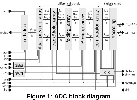
The converter under investigation, a 6-bit 330MS/s differential folding ADC. It is implemented in a 0.3?m standard CMOS process. The layout occupies 0.1mm2 of silicon, contains 1050 transistors. 75% of the silicon area is dedicated to analogue circuitry.
The analogue section of the converter comprises a resistor ladder to generate the differential reference voltages, two amplifier arrays, a track and hold array, and a comparator array, as illustrated in Figure 1. Two groups of signal paths can be identified. The first group of signals contributes to the calculation of the four lower bits, d0 to
d3, while the second group determines the two higher bits
d4 and d5. For each group the subcircuits contained in the five arrays (Figure 1) are identical, allowing a reduction in the number of faults to simulate, as explained in section 4. To further reduce fault simulation times, the digital encoding block and the clock generator have been replaced by simple behavioural models.
refladder
dual_preamp_array track&hold_array
Preamp_array
comparator_array
encoding
clk pwd
bias
vss vdda vddd iref ladn inp inn ladp
pwd test curtest
divorby8
clkin clkffadc clkchan d1_<0:5>
midlad
6 6
19 10
38 10
38
6
16 3
16
folding_array
6
8
d2_<0:5>
differential signals
e1..19 f1..19 g1..4 h1..8 i1..16 fmsb
fms1,2 fos1,2
imsb ims ios hmsb hms hos gmsb
gms gos emsb
ems1,2 eos1,2
ref1..19
[image:2.595.55.281.544.709.2]digital signals
Figure 1: ADC block diagram
4. Fault Simulation of ADC
Fault sim ulations usually facilitate test quality com putation, DfT optimisation, and the identification of difficult to test and difficult to detect faults [7]. Within this work, the approach has been adopted to ex tract inform ation on failure m odes for ADCs.
A fault list has been ex tracted from the layout based on a detailed investigation into DSM failure m echanism s. Fault simulation models used (gate-oxide shorts, floating gate transistors, narrow MOS transistors and others) will be listed briefly in the final paper to provide essential background information.
The ADC’s fault list obtained contains 4469 faults and includes probability data. As m entioned above, the converter contains a large num ber of identical sub-circuits com posing two types of signal paths. Hence only faults affecting one lower bit signal path and one upper bit signal path are sim ulated. The reduced fault list contains 629 candidates (Figure 2). Taking fault probability data into account, the group of short (open) faults affects 94% (6%) of faulty devices due to defect statistics applied.
629 Faults
448 SHORTS; 70%
4 R_OPENS; 1% 18 OPENS; 3%
4 Wlow; 1% 52 FGT; 8% 49 SDP; 8%
48 GOS; 8%
6R_SHORTS;1%
various open faults
12% 6 shorts between resistors; 1% 49 high-ohmic drain-source; 8% shorts
4 narrow MOSTs; 1% 4 resistor opens; 1%
Figure 2: ADC fault set
4.1 Fault Simulation Analyses
been acceptable, the use of behavioural m odels for non-fault-affected analogue circuitry, however, is ex pected to reduce the sim ulation tim e dram atically.
Ongoing sim ulations are perform ed to evaluate dynamic failure m odes, where the converter is fault simulated against a typical functional test.
5. Failure Modes
Data analysis has been based on the use of fault coverage (FC) and weighted fault coverage (WFC), taking the fault probability into account [8], defined as:
% 100 *
% 100
1 1
1 ? ? ?
?
?
?
?
? ? ?
N
n N
n N
n
Wn Wn Dn WFC N
Dn FC
Dn: binary detection function
with 0 undetected; 1 detected fault n out of N faults Wn: num ber of circuits containing fault n
Figure 3 sum m aries som e of the data obtained. The fault coverage is illustrated for com paring offset, gain and CW against thresholds determined by the use of Monte Carlo process variation sim ulations. Estim ating INL as m entioned above is com m on practise in som e BIST techniques for ADCs. Furtherm ore, coverages for average current m easurem ents during ram p simulation (Meas) and monotonicity (mono), and the accum ulated FC (Accu) test are given.
The illustration below also presents data on the hardness of the failure m ode ex hibited. A significant proportion of short faults are only causing test failures when m odelled by a low-ohmic resistor (1? to 20? ), but remain within the tolerance window for higher-ohmic shorts (1k? ). Applying a realistic test threshold (com puted by Monte -Carlo simulations taking m easurem ent resolution and other contributing factors into account), leads to an accum ulated fault coverage of m ore than 82%. Widening the test thresholds by 200% will still lead to a FC of m ore than 75%. The m easurem ent m ost sensitive to the threshold applied is the CW com putation.
Further explanations and coverage figures (FC and WFC) for power-down tests and others will be included in the final paper.
0% 10% 20% 30% 40% 50% 60% 70% 80% 90%
Offset Gain CW INL Mono Meas Accu. Tests
FC
Short faults detected for low resistance only Realistic test threshold (100%)
Widened threshold (200%)
Widened threshold (300%)
Figure 3: ADC failures
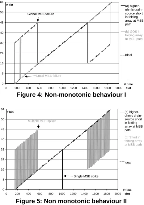
Figures 4 to 8 illustrate som e of the failure m odes observed for the ram p input stimulus.
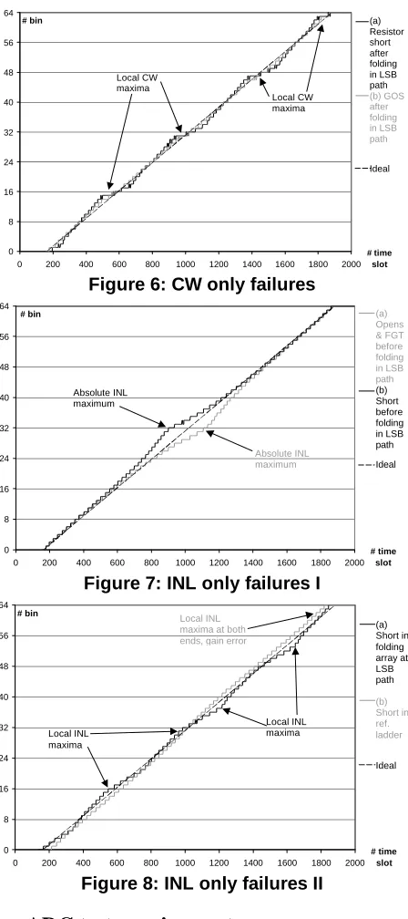
The final paper will contain detailed descriptions on faults causing single test failures, for example CW only, and fault diagnosis capabilities. As depicted in Figure 7 and Figure 8, evaluating the number of local CW maxima allows some level of fault location. Also parametric faults will be addressed, leading towards a discussion on Design-for-Robustness for analogue circuitry.
0 8 16 24 32 40 48 56 64
0 200 400 600 800 1000 1200 1400 1600 1800 2000
# time slot
# bin Ideal
GOS in foldin g array MSB path
SDP in foldin g array MSB path (a) higher-ohmic drain-source short in folding array at MSB path
(b)GOS in
folding array at MSB path
Ideal Global MSB failure
[image:3.595.319.536.74.240.2]Local MSB failure
Figure 4: Non-monotonic behaviour I
0 8 16 24 32 40 48 56 64
0 200 400 600 800 1000 1200 1400 1600 1800 2000
# time slot
# bin Short
in foldin g array MSB path Short in foldin g array MSB path (a) higher-ohmic drain-source short in folding array at MSB path
(b) Short in folding array at MSB path
Ideal Multiple MSB spikes
Single MSB spike
[image:3.595.312.545.381.712.2]0 8 16 24 32 40 48 56 64
0 200 400 600 800 1000 1200 1400 1600 1800 2000
# time slot
# bin Resist
[image:4.595.57.281.71.575.2]or short in foldin g array GOS in foldin g array (a) Resistor short after folding in LSB path (b) GOS after folding in LSB path Ideal Local CW maxima Local CW maxima
Figure 6: CW only failures
0 8 16 24 32 40 48 56 64
0 200 400 600 800 1000 1200 1400 1600 1800 2000
# time slot
# bin Open
faults and FGT before foldin g array Short fault before foldin g array (a) Opens & FGT before folding in LSB path (b) Short before folding in LSB path Ideal Absolute INL maximum Absolute INL maximum
Figure 7: INL only failures I
0 8 16 24 32 40 48 56 64
0 200 400 600 800 1000 1200 1400 1600 1800 2000
# time slot # bin Short after foldin g array short in refere nce ladder (a) Short in folding array at LSB path (b) Short in ref. ladder Ideal Local INL maxima Local INL maxima Local INL
maxima at both ends, gain error
Figure 8: INL only failures II
6. ADC test requirements
To sum m arise preliminary results it can be stated that 85 to 90% of faults ex hibit failure m odes detectable by DC specification m easurem ents. While the m ajority of faults caused by process induced spot defects ex hibit hard functional failure (missing codes, ex cessive DNL, non -m onotonic behaviour), a large portion of the fault set, about 30 to 40%, will result in parametric functional failure only. Ex amples have been shown, indicating that process induced faults, such as shorts, opens, FGT, GOS etc can in fact cause perform ance to m arginally fail specification, such as DNL or INL.
7. Conclusions & future work
The paper has identified failure m odes of the target ADC. It has been shown, that a large proportion of traditionally considered shorts and opens and som e other device oriented faults, such as GOS, FGT or SDP, contribute to failure m odes missing performance specifications only m arginally. Expected test coverage figures against the layout ex tracted fault set have been presented, that provide key data required for test program optimisation. BIST techniques published recently are ex pected to achieve fault coverages of about 80 to 90%.
More detailed analysis is required to pinpoint the prime test objective and potential quality problem s. Detailed and tim e-consuming structural DfT studies utilising fault sim ulation environm ents seem to rem ain the only approach leading to a better understanding of analogue circuit specific failure m odes. Com puter-aided test tools currently under developm ent will reduce required m an-time, and new test coverage figures m ay eventually pave the way for test quality com putation. Autom ating the test program generation and DfT optimisation itself, however, rem ains a challenge.
Ongoing and future work is addressing dynamic tests to further im prove the understanding of failure m odes. This m ay result in the use of defect-oriented, faster and cheaper tests which m ay also be supported by on -chip test support structures. Also work is required on the definition of appropriate coverage m etrics.
Acknowledgements
This work has been supported by EPSRC through the "ATOM" project (Analogue and Mix ed Signal Integrated Circuit Test Support for High Quality, Low Cost Manufacture) - EPSRC GR/M7553 and through EC Framework 4 program 'ASTERIS' ref: ESPRIT 26354.
References
[1] Semiconductor Industry Association: 'International Technology Roadmap for Semiconductors, 1999 Edition', 1999
[2] A. Lechner, M. Burbidge, A. Richardson & B. Hermes: '3DB challenge for DfT, DfM, DOT & BIST integration into analogue and mix ed signal ICs', Latin American Test Workshop, LAT01, 11-14th Feb. 2001, Cancun, Mex i co [3] A. Lechner, J. Ferguson, A. Richardson & B. Hermes: 'A
partial built-in self-test for a high performance automatic gain control circuit', Design, Automation and Test in Europe, DATE99, 9-12th March 1999, Munich, Germany, pp.232-238
[5] A. Frisch & T. Almy: 'HABIST: histogram-based analog built in self test', IEEE International Test Conference, ITC97, 3-5th Nov. 1997, Washington, DC, USA, pp. 760 -767
[6] M. Renovell, F. Azais, S. Bernard & Y. Bertrand: 'Hardware resource minimization for histogram-based ADC BIST', 18th IEEE VLSI Test Symposium, VTS00, 30th April - 4th May 2000, Montreal, Quebec, Canada, pp.247-252
[7] A. Lechner, A. Richardson, B. Hermes & M. Ohletz: 'A design for testability study on a high performance automatic gain control circuit', 16th IEEE VLSI Test Sym posium, VTS98, 26-30th April 1998, Monterey CA, USA, pp.376-385