Switched Capacitor Biquad Filter Using CDTA
Meeti Dehran1, Indu Prabha Singh1, Kalyan Singh2, Rabindra Kumar Singh3
1Department of Electronics and Communications Engineering, Shri Ramswaroop Memorial Group of Professional Colleges (SRMGPC), Lucknow, India
2Department of Physics and Electronics, R.M.L. University, Faizabad, India
3Department of Electrical and Electronic Engineering, Kamla Nehru Institute of Technology (KNIT), Sultanpur, India Email: [email protected], [email protected]
Received July 20, 2013; revised August 20, 2013; accepted August 27, 2013
Copyright © 2013 Meeti Dehran et al. This is an open access article distributed under the Creative Commons Attribution License, which permits unrestricted use, distribution, and reproduction in any medium, provided the original work is properly cited.
ABSTRACT
A switched capacitor biquad filter using current differencing transconductance amplifier (CDTA) is presented in this paper. The proposed circuit employs only one CDTA, two virtually grounded capacitors and one switched capacitor. It is a resistorless circuit, so it is beneficial to IC implementation in terms of space consideration. The proposed circuit is a second order single input multiple output (SIMO) current-mode filter. This filter can simultaneously realize all basic filter functions high pass, low pass and band pass responses without any component-matching conditions. All the active and passive sensitivities are low. The natural angular frequency (ω0) and quality factor (Q) of proposed filter can be electronically controlled. Owing to current mode operation it consumes less power. PSPICE simulation results are used to verify the theoretical analysis.
Keywords: Current Differencing Transconductance Amplifier (CDTA); Biquad Filter; Current-Mode Circuit
1. Introduction
Since the introduction of the current differencing trans-conductance amplifier (CDTA) in 2003, it has been ac- knowledged to be a versatile current-mode active build- ing block in designing analog circuits [1]. This device with two current inputs and two kinds of current output provides an easy implementation of current-mode active filters [2]. It also exhibits the ability of electronic tuning by the help of its transconductance gain (gm). All these
advantages together with its current-mode operation na- ture make the CDTA a promising choice for realizing the current-mode filters. As a result, a variety of CDTA ap- plications has also been considered by various research- ers.
The work in [2] introduces universal biquad filters which can simultaneously realize lowpass (LP), highpass (HP) and bandpass (BP) current responses. However, they suffer from the use of a large number of passive components. On the other hand, a lowpass filter circuit using CDTAs is proposed in [3]. However, this configu- ration is restricted for only lowpass transfer function de- sign and it also requires an additional passive resistor. In [4], the CDTA-based current-mode single-input three- output filter is reported. It permits the realization of only three basic filter functions LP, BP, and HP responses
simultaneously at high impedance output. While the cir- cuit proposed in [5] requires four CDTAs, and an exter- nal passive resistor for its realization. In [6], a universal current-mode biquad, providing four basic transfer func- tions (low-pass, band-pass, high-pass, and band-reject) simultaneously is described. However, this circuit labors with the following drawbacks: 1) only the output current of the low-pass section flows to an independent load. All the remaining output currents flow through the working impedances and thus they cannot be directly utilized without negative influence on the filter behavior. 2) The additional resistor R3 does not represent any increase of the filter versatility and thus it can be removed from the filter structure without decreasing its functionality. The paper published in [7] employed two CDTA to perform all three basic filter functions. Second order filter using single CDTA is published in [8,9]. The paper proposed in [8] provides only BP and HP outputs or LP and BP re- sponses after interchanging RC network to CR. The filter introduced in [9] uses single CDTA and provides several transfer functions depending on the position of applied input current, but at low frequency.
vantage of using switched capacitor instead of a resistor that is beneficial to IC implementation in terms of space consideration. The proposed circuit can be used as high pass, low pass, and band pass filter. PSPICE simulation results are used to verify the performance of the proposed circuit.
2. CDTA
Digital signal processing is becoming increasingly more powerful while advances in IC technology provide com- pact efficient implementation of its algorithms on silicon chips. Although many types of signal processing have indeed moved to digital domain, analog circuits are fun- damentally necessary in many of today’s complex, high performance systems. This is caused by the reality that naturally occurring signals are analog. Therefore analog circuits act as a bridge between the real world and digital systems. In the beginning, operational amplifiers were the main building blocks for analog circuit design. Un- fortunately, their limited performance such as bandwidth, slew-rate etc. led the analog designer to search for other possibilities and other building blocks. As a result, new current-mode active building blocks such as Operational Transconductance Amplifiers (OTA), second generation Current Conveyors (CCII), Current-Feedback Op-Amps (CFOA), Differential Voltage Current Conveyor (DV- CC), Differential Difference Current Conveyor (DDCC), third-generation Current Conveyor (CCIII), Dual X Cur- rent Conveyors (DXCCII), Current Controlled Current Conveyors (CCCII), Current Differencing Buffered Am- plifier (CDBA) And Current Differencing Transconduc- tance Amplifier (CDTA) receive considerable attention due to their larger dynamic range and wider bandwidth. Employing these new active elements for analog design and using CMOS technology for implementation, the circuit designers obtained new possibilities to solve their problems. CDTA device is a synthesis of the well-known advantages of the CDBA and an output transconductance amplifier to facilitate the implementation of current- mode analog signal processing.
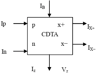
The electrical symbol of the CDTA is shown in Figure 1. The terminal relation of the CDTA can be character- ized by the following set of Equation (1).
p x+
CDTA
n x
p x+ CDTA n x− Ip
In
Iz IB
IX+
IX−
Vz
Figure 1. Electrical symbol of CDTA.
0 0 0 0
0 0 0 0
1 1 0 0
0 0 0 0
p p
n n
z z
x m
V I
V I
I V
I g
0
p n
z p n
x m z
x m z
V V
I I I
I g V
I g V
(1)
Where
P and n are input terminals; z and ±x are output terminals; gmis the transconductance gain;
And Zzis external impedance connected at the terminal
z.
According to above equation, the current flowing out of the terminal z (Iz) is a difference between the currents
through the terminals p and n (Ip- In). The voltage drop
at the terminal z is transferred to a current at the terminal x (Ix) by a transconductance gain (gm), which is electroni-
cally controllable by an external bias current (IB). These
currents, which are copied to a general number of output current terminals x, are equal in magnitude but flow in opposite directions.
The (CDTA) is composed of a unity-gain current source controlled by the difference of two input currents and a multi-output transconductance amplifier providing elec- tronic tuning ability through its transconductance gain (gm). Therefore, this device is quite suitable for the syn-
thesis of current-mode filters with electronically tunabil- ity properties. Moreover, the use of the CDTA as an ac- tive element provides the circuit implementations with a reduced number of passive elements, thereby leading to compact structures in some applications. All these ad- vantages together with its current-mode operation nature make the CDTA a promising choice for implementing the current-mode continuous-time signal processing cir- cuits consecutively.
Figure 2 shows a CMOS realization of the CDTA ele- ment [10]. The transistors M1 to M17 form the input DCCCS stage and M21 to M28 form the dual-output transconductor stage Aspect ratios of the transistors in Figure 2 are given in Table 1.
3. Proposed Circuit
The proposed current-mode multifunction filter employ- ing CDTA, two grounded capacitors and a switched ca- pacitor is shown in Figure 3.
[image:2.595.97.256.600.723.2]Vd d
M 1 2 M 1 1
M 0 4
M 0 5
M 0 6 M 0 8 M 0 9
M 0 7
M 1 0
M 0 2
M 0 3 M 0 1 P
M 1 7 M 1 6 M 1 5
M 1 3 M 1 4
M 2 7
M 2 6
M 2 3 M 2 1
X -X +
M 2 2 M 2 4 IB
M B M 2 5
M 2 8 n
z
V ss
[image:3.595.64.532.86.350.2]V ss
[image:3.595.312.540.396.603.2]Figure 2. CDTA CMOS implementation from [10].
Table 1. Aspect ratios of the transistors.
M1 = 70 µm/0.7 µm M15 = 35 µm/0.7 µm
M2 = 70 µm/0.7 µm M16 = 35 µm/0.7 µm
M3 = 70 µm/0.7 µm M17 = 35 µm/0.7 µm
M4 = 28 µm/0.7 µm M21 = 28 µm/0.7 µm
M5 = 28 µm/0.7 µm M22 = 16 µm/0.7 µm
M6 = 28 µm/0.7 µm M23 = 28 µm/0.7 µm
M7 = 42 µm/0.7 µm M24 = 16 µm/0.7 µm
M8 = 10.5 µm/0.7 µm M25 = 56 µm/0.7 µm
M9 = 10.5 µm/0.7 µm M26 = 59 µm/0.7 µm
M10 = 42 µm/0.7 µm M27 = 56 µm/0.7 µm
M11 = 10.5 µm/0.7 µm M28 = 56 µm/0.7 µm
M12 = 98 µm/0.7 µm MB = 7 µm/0.7 µm
M13 = 10.5 µm/0.7 µm M30 = 50 µm/0.7 µm
M14 = 10.5 µm/0.7 µm M31 = 50 µm/0.7 µm
duces the required space for the fabrication. The SC is compatible with CMOS technology. The proposed circuit is able to perform the basic filter functions i.e. low pass, high pass, band pass. The low pass, high pass and band pass current outputs have been shown in Figure 3. From routine calculations for the proposed filter, the current responses can be given by:
P
N
Z
X‐
X+ ILP
IHP
C1
IBP
C2
C3
I in
Ø1
Ø2
CDTA
Figure 3. Biquad filter using CDTA element.
1 2 2
1 1 2
1
m
LP in
m g RC C
I I
g
S S
RC RC C
(2)
1 2
1 1 2
1
1
BP in
m S RC
I I
g
S S
RC RC C
[image:3.595.65.282.400.640.2]2
2
1 1 2
1
HP in
m S
I I
g
S S
RC RC C
(4)
Bandwidth (BW), natural frequency (ω0) and quality factor (Q)are given by
1 0
1 1 2 2
1
, m ,
m
g C
BW Q g R
RC C C R C
(5)
From Equation (5), the parameter ω0 can be controlled by transconductance gm independently of bandwidth. The
transconductance values can be changed through adjust- ing the biasing current of the CDTA.
From the expression of Equation (5), the sensitivities of ω0 and Q to variations in various parameters is given as
0 0
1 2,
1 2
,
,
1, 1,
2 2
1 1
,
2
, 2
2
1 m m
Q g
g C C R
Q Q
C R C
S S S
S S
(6)
Hence all the sensitivities are low as calculated in Equation (6).
The value of the capacitor C3 used in switched capaci- tor is calculated using the formula given as
3
1
C Rf
(7)
Where, R is the equivalent resistance value of the switched capacitor and f is the frequency of clock signal (Φ1) and (Φ2), applied at two mosfets (M30, M31) of switched capacitor.
4. Simulation Results
The performance of the proposed filter is verified using the simulation in PSpice. According to the analysis from Sections 2 and 3, the single input excitation is given. The CDTA model employing the n-well CMOS process TSMC 0.35 mm is used. The transconductanceis set to 888 µS via a bias current of 40 µA.
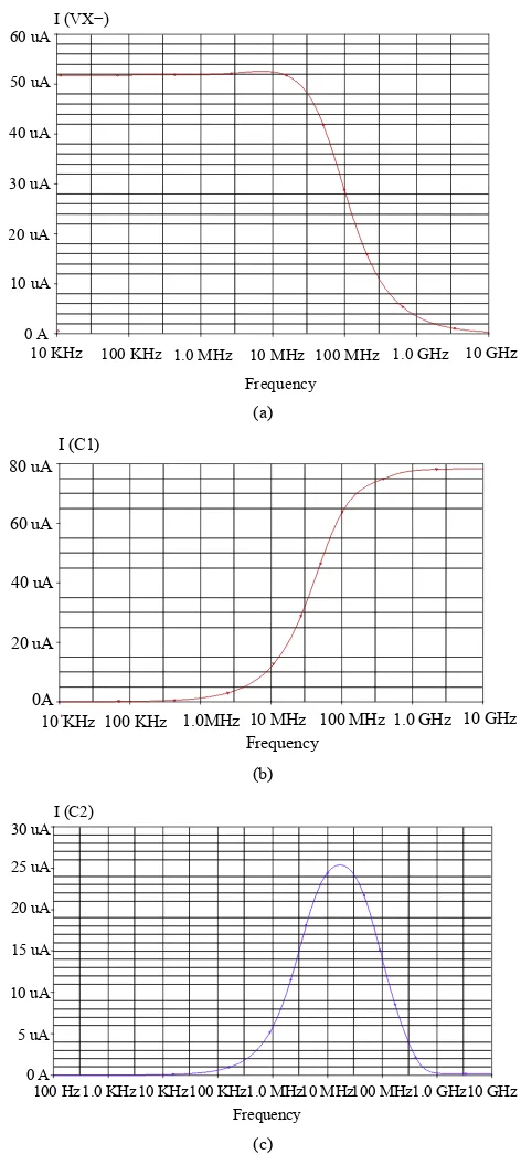
As an example design, the capacitors C1 = C2 = 10 pF, C3 = 2.96 pF and the biasing current Ibias = 40 μA are given. This setting has been designed to obtain the LP, BP and HP, filter responses. The simulated responses of the BP, LP and HP of the proposed filter are shown in Figure 4. Both the natural frequency and the quality fac- tor are in accordance with the proposed values.
5. Conclusion
A 2nd-order single input multiple output (SIMO) cur- rent-mode filter employing a single CDTA is described in the paper. The natural angular frequency ω0and the bandwidth ω0/Q can electronically be controlled by ad-
Frequency
10 KHz 100 KHz 1.0 MHz 10 MHz 100 MHz 1.0 GHz 10 GHz I (VX−)
10 uA 20 uA 30 uA 40 uA 50 uA 60 uA
0 A
(a)
Frequency
10 KHz 100 KHz 1.0MHz 10 MHz 100 MHz 1.0 GHz 10 GHz 0A
20 uA 40 uA 60 uA 80 uA
I (C1)
(b)
Frequency
100 Hz 1.0 KHz 10 KHz100 KHz1.0 MHz 10 MHz 100 MHz 1.0 GHz10 GHz 0 A
5 uA I (C2)
10 uA 30 uA
25 uA
20 uA
15 uA
[image:4.595.304.540.81.603.2](c)
Figure 4. Response of biquad filter using CDTA element. (a) Low pass response; (b) High pass response; (c) Band pass response.
justing the transconductance gain gm of the CDTA. The
rameter ω0. The switched capacitor has good linearity. The PSPICE simulation results demonstrate the close agreement with the presented theory.
REFERENCES
[1] D. Biolek, “CDTA-Building Block for Current-Mode Ana- log Signal Processing,” Proceedings of European Con- ference on Circuit Theory and Design (ECCTD), Poland, 1-4 September 2003, pp. 397-400.
[2] D. Biolek and V. Biolkova, “Universal Biquad Using CDTA Elements for Cascade Filter Design,” Proceeding of 7th International Multiconference on Circuits, Systems Com- munications and Computers (CSCC), Athens,7-9 July 2003, pp. 8-12.
[3] A. T. Bekri and F. Anday, “Nth-Order Low-Pass Filter Employing Current Differencing Transconductance Am- plifiers,” Proceeding of the 2005 European Conference on Circuit Theory and Design, Cork, 28 August-2 Sep- tember 2005, pp. 193-196.
[4] D. Biolek and V. Biolkova, “CDTA-C Current-Mode Uni- versal 2nd Order Filter,” Proceeding of the 5th WSEAS International Conference on Applied Informatics and Com- munications, Malta, 15-17 September 2005, pp. 411-414. [5] W. Tanjaroen, T. Dumawipata, S. Unhavanich, W. Tangs-
rirat and W. Surakampontorn, “Design of Current Differ- encing Transconductance Amplifier and Its Application to Current-Mode KHN Iquad Filter,” Proceeding of ECTI- CON, Ubon Ratchathani, 10-13 May 2006, pp. 497-500. [6] D. Prasad, D. R. Bhaskar and A. K. Singh, “Universal
Current-Mode Biquad Filter Using Dual Output Current
Differencing Transconductance Amplifier,” International Journal of Electronics and Communications, Vol. 63, No. 6, 2008, pp. 497-501.
[7] A. Uygur and H. Kuntman, “Design of a Current Differ- encing Transconductance Amplifier (CDTA) and Its Ap- plication on Active Filters,” SIU’2005: IEEE 13th Signal Processing and Communication Applications Conference, Kayseri, 16-18 May 2005, pp. 340-343.
[8] N. A. Shah, M. Quadri and S. Z. Iqbal, “Current Mode Multifunction Filter Using Current Differencing Trans- conductance Amplifier,” Indian Journal of Pure & Ap- plied Physics, Vol. 45, No. 9, 2007, pp. 767-769.
[9] D. Biolek, V. Biolkova and Z. Kolka, “Single-CDTA (Cur- rent Differencing Transconductance Amplifier) Current- Mode Biquad Revisited,” WSEAS Transactions on Elec- tronics, Vol. 5, No. 6, 2008, pp. 250-257.
[10] D. Biolek, E. Hancioglu and A. U. Keskin, “High-Perfor- Mance Current Differencing Transconductance Amplifier and Its Application in Precision Current-Mode Rectifica- tion,” International Journal of Electronics and Commu- nications, Vol. 62, No. 2, 2008, pp. 92-96.
[11] M. Bhusan and R. W. Newcomb, “Grounding of Capaci- Tors in Integrated Circuits,” Electronics Letters, Vol. 3, No. 4, 1967, pp. 148-149.
[12] K. Pal and R. Singh, “Inductor Less Current Conveyor All Pass Filter Using Grounded Capacitors,” Electronics Letters, Vol. 18, No. 1, 1982, p. 47.
![Figure 2. CDTA CMOS implementation from [10].](https://thumb-us.123doks.com/thumbv2/123dok_us/7864635.737593/3.595.64.532.86.350/figure-cdta-cmos-implementation-from.webp)