http://dx.doi.org/10.4236/jemaa.2016.84009
New 3D Aware Formulation of MoM-GEC
Method for Studying Planar Structures
with Vertical Sources
Oueslati Basma, Ben Salah Taha, Larbi Chiraz, Aguili Taoufik
Communication System Laboratory Sys’Com, National Engineering School of Tunis, University Tunis El Manar, Tunis, Tunisia
Received 9 March 2016; accepted 24 April 2016; published 27 April 2016
Copyright © 2016 by authors and Scientific Research Publishing Inc.
This work is licensed under the Creative Commons Attribution International License (CC BY).
http://creativecommons.org/licenses/by/4.0/
Abstract
This paper proposes a generalization of the MoM-GEC method [1] needed for studying planar structures excited with a source located at perpendicular plan relative to circuit plan. A general formulation is detailed to allow modeling excitation of a planar structure with one or more sources located in plans other than the circuit plan. The numerical approach elaborated is based on the definition of new admittance operators and rotational transformations describing the tran-sition from one plan to another. To validate this approach, we consider the case of a single source located in the perpendicular plan to the circuit.
Keywords
Admittance Operator, MoM-GEC 3D, Discontinuities, Vertical Source
1. Introduction
Studying of microwave planar circuits is based on EM characterization of the structure via determination of electrical (E) and magnetic (H) fields and the electric current density J using Maxwell equations. To solve these equations, iterative methods are used (FDTD [2][3] and FEM [4][5]) providing accurate results but requiring a relatively heavy calculation time [6]. To overcome this disadvantage, integral methods have been proposed. Integral equations introduce an excitation term in the integral formulation of an electromagnetic problem that needs to establish an appropriate mathematical model: source model [7].
defined in the perpendicular plan to the circuit. The source can be considered as a discontinuity causing the cre-ation of higher order modes at the border source/circuit [10]-[15]. This discontinuity can be corrected by using a coupling quadripole [8] [16]-[18]. That generates an additional computing time. Considering the fundamental mode of the access line can be an optimized solution which allows us to have a perfect adaptation between source and circuit [19][20].
Localized source remains a theoretical and relatively simple model to describe studied structure. Such model, is not fully consistent with actual excitations located in another plan than the circuit which favors the extended source, hence the importance of our study.
Our goal is to develop an exact source method based on MoM-GEC method for studying planar structures ex-cited by sources located in any other plan. We first establish a general formulation for the case of N sources. We verify, then the accuracy of the hypothesis of sources simplification: localized planar sources.
3D extension of MoM-GEC method has not been really focused on in previous work. Related work mainly includes Hamdi et al. work in [13]. However, this work focused on input impedance and scattering matrix eval-uation rather than a full EM characterization. In our study, we define new admittance operators to bind excita-tion sources to electrical quantities defined in the circuit plan and thus help calculate EM fields accurately. We also introduce a new rotational transformation describing the transition from one plan to another. The determi-nation of these operators is important because it allows us to perform three-dimensional calculation while keep-ing homogeneous the MoM-GEC method (decomposition of operators on the TE and TM modes).
In this paper, input impedance, current density and electric field distribution are evaluated and discussed in the case of a single vertical source. Results are compared to commercial software HFSS and CST. A couple of structures are studied: microstrip short-circuited line and microstrip open circuit line as an application.
This paper is organized as follows: we start presenting the new approach in the case of N sources by exposing the general formulation of integral equations to determine the admittance matrix. Then, we detail the formula-tion and the determinaformula-tion of input admittance (yin) in the case of a single extended source located at the per-pendicular plan to circuit. In Section 4, we focus on determining admittance operators. Finally, in Section 5 we present different simulations results obtained for the two studied structures.
2. New Formulation of MoM-GEC Method for 3D Structures
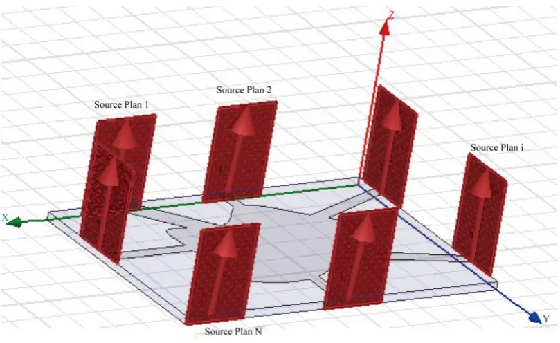
[image:2.595.112.517.459.707.2]In this section, we introduce and explain the general formulation for 3D structures by considering the case of N-ports (N sources) located at perpendicular plans to the circuit. Figure 1 shows the general structure excited by
voltage sources (E01,E02,,E0N). The electromagnetic analysis of this structure consists in solving an integral
equation expressing the boundary conditions of electromagnetic fields of sources and circuit plans. This equa-tion has the following form:
( )
.L f =g (1)
where L is an integro-differential operator, g is the excitation source and f is the unknown to be determined. In this work, L is an admittance operator, f is the electric field E tangential to the circuit plan and g represents the excitation sources. The method consists in solving this equation by the Galerkin method (a variety of the MoM method) to determine the electric field E and deduce the input admittance Yin matrix
The circuit is printed on a dielectric substrate of relative dielectric constant εr with a thickness h. N trans-mission lines feed the structure defining N discontinuities. Each transtrans-mission line is excited with a vertical port. Discontinuities at port level is overcome by considering fundamental mode of the transmission line.
To characterize this discontinuity, we used the formalism of admittance operator and assume that excitation sources are totally independent and completely decoupled (electromagnetic coupling) for each other [21][22]. It would be necessary to determine with precision the fundamental mode of the attachment lines to ensure good adaptation.
The electromagnetic quantities in source plans (from P1 to PN) and planar circuit (c) are expressed in
follow-ing relations (Equation (2)):
01 11 01 1 0 1,
0 1 01 0 ,
0 1 01 0 ,
,1 01 , 0 ,
ˆ ˆ ˆ
ˆ ˆ ˆ
ˆ ˆ ˆ
ˆ ˆ ˆ
N N c
i i iN N i c
N N NN N N c
c c N N c c
J Y E Y E Y E
J Y E Y E Y E
J Y E Y E Y E
J Y E Y E Y E
= + + + = + + + = + + + = + + + (2) where: oi
J (i = 1 to N): current density of the source (i).
oi
E (i = 1 to N): Electric field of the source (i).
ˆ
ij
Y (i = 1 to N + 1, j = 1 to N + 1): Admittance operators with the (N + 1)th plan is the circuit plan. E and J are the electric field and the current density defined in the circuit plan.
The admittance operators Yˆij define the relationship between the electric fields of TE and TM modes from the jth plan and the current density generated by these modes on the ith plan provided that all sources k # j are switched off and the circuit plan is metallized. These Yˆij can be determined by applying the superposition
theorem to the Equation (2) and decomposing these operators on a homogeneous basis (TE and TM) associated to each plan defining the different electromagnetic quantities.
If
( )
fmn ( )j and( )
fpq ( )i are a decomposition orthonormal basis of the electric field and current density de-fined on the plans i and j, then for; i=1,,N and j=1,,N, Yˆij can be expressed as follows:( ) , ( ) ,
, ,
ˆ i TE TM TE TM j TE TM.
ij pq mn pq mn
mn pq
Y =
∑∑
f y f (3)For modeling the electric field E of the circuit plan, we choose test functions of electric field type ϕi. The test functions are assumed to be virtual sources defined in the circuit plan. On this basis, the electric field is written as follows:
1 . K
k k k
E xϕ
=
=
∑
(4)Test functions satisfy the boundary conditions of the circuit plan. They are zero on the metal and non-zero on the dielectric. And conversely, the current density J defined on the circuit plan is zero on the dielectric and non- zero on the metal. Therefore, the test function ϕk and the current density J satisfy the following relationship:
0.
k J
ϕ = (5)
The application of the Galerkin method to the Equation (2) involves projecting the first N equations respec-tively on the unitary sources functions from e01 to e0N , which gives us a first sub system. Also, we project the (N + 1)th equation on the various test functions which gives us a second sub system.
We suppose that: E0i =V e0i 0i and J0i =I j0i 0i. With e0i j0i =1.
Considering the orthonormalization relationships verified by these unitary sources: (where δij is the dirac function) and the relationship between current density and test functions, we obtain the following matrix rela-tionship:
01 11 1 01
0 1 0
.
N
N N NN N
I y y V
I y y V
=
(6)
With:
1
.
ij ij i j
y =Y −C A B− (7)
0 ˆ 0 .
ij i ij j
Y = e Y e (8)
( )
, i ˆN1,N 1 k .A i k = ϕ Y + +ϕ (9)
( )
0 1, 0 0( )
1 1
ˆ ; 1, ,
K K
n j N n n n n
n n
B j V ϕ Y + e V B j j N
= =
= −
∑
= −∑
= (10)( )
0 0 1, 0( )
1 1
ˆ ; 1, ,
K K
n n N n i n n
n n
C i V e Y + ϕ V C i i N
= =
= −
∑
= −∑
= (11)The determination of the admittance matrix
( )
, 1, , ij i j N y= involves calculating of the different admittance op-erators Yˆij. In order to model the electric field E, it is enough to determine the coefficients of test functions xk.
The vector
(
1, , , ,)
t
k K
X = x x x is written in the following form (Equation (12)): 1
0i i i
X = −
∑
V A B− (12)In this section, we presented a general formulation of the problem by taking the case of N vertical sources. By applying the Galerkin method, we determined the admittance matrix binding current density and E field. This matrix is characterized by new admittance operators describing the transition from one plan to another. To vali-date our approach, we develop in this paper the case of a single vertical source that is the subject of the next sec-tion.
3. Single Vertical Source Case
The vertical source located at perpendicular plan to the circuit is the most used excitation source in real condi-tions. We focus now on the study of a single vertical source located at the perpendicular plan to the circuit. We start presenting the studied structures. Then, we detail the determination of the admittance operators.
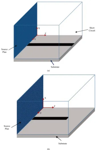
3.1. Studied Structures
(a)
[image:5.595.142.494.81.608.2](b)
Figure 2. Studied structures: (a) Microstrip short-circuited line; (b) Microstrip open circuit line.
second structure allows us to verify the boundary conditions and to ensure the validity of the numerical ap-proach.
Table 1 and Table 2 illustrate the dimensions of the two structures enclosed in a box. With: ε =r 1 and freq = 3.5 GHz,
lp: length of the microstrip line,
ls: length of the dielectric substrate,
Table 1. Microstrip short-circuited line dimensions.
Length Width Height
Line lp = λ/2 wp=2 mm≈λ 40 -
Dielectric substrate ls = λ/2 a=12.7 mm≈λ7 h0=1.27 mm≈λ70
Box lb = λ/2 a=12.7 mm≈λ7 h=11.43 mm≈2λ15
Table 2. Microstrip open circuit line dimensions.
Length Width Height
Line lp = λ/2 w=2 mm≈λ 40 -
Dielectric substrate ls = λ a=12.7 mm≈λ7 h0=1.27 mm≈λ70
Box lb = λ a=12.7 mm≈λ7 h=11.43 mm≈2λ15
wp: width of the microstrip,
a: width of the box/dielectric substrate, h0: thickness of the dielectric substrate, h: thickness of the box.
By using the generalized equivalent circuit method, we can model each of the two structures of the Figure 2 with the following equivalent circuit (Figure 3).
The circuit is excited by a single source of electric field type. This source is defined by a unitary function
( )
1 ,
e x y , such as: e j1, 1 =1 and j1 is the current density associated to e x y1
( )
, at the plan (xoy). Theunitary source e1 and the dual current j1 are written as follows:
1 .
d
d d
E e
E J
= (13)
1 .
d
d d
J j
E J
= (14)
With: Ed is the electric field of the straight section and Jd is the dual current density
.
d = d∧
J H z (15)
To determine the electric field Ed, we calculate the fundamental E field of a microstrip line having infinite length [13][19][20].
3.2. The Input Admittance of a Discontinuity Port
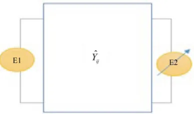
Using the formulation of the source method developed in the Section 2, the current densities of the source and the circuit are associated to the corresponding electric fields by the admittance operators:
1 11 1 12 2
2 21 1 22 2
ˆ ˆ
ˆ ˆ
J Y E Y E J Y E Y E
= +
= +
(16)
Applying the same procedure in (2), the Galerkin method is used to solve Equation (16) while taking into ac-count the boundary conditions of electromagnetic fields on the circuit plan. The first step in the Galerkin method is to define test functions
( )
1, ,
i i K
ϕ
= to model the electric field E2 (Equation (17)).2 1
. K
i i i
E xϕ
=
=
∑
(17)The test functions
( )
1, ,
i i K
Figure 3. Equivalent circuit of the studied structure.
plan (xoz) (Equation (18)).
( )
( )
(
)
( )
(
)
2 1 π
cos 2
, ; 0, ,
2 2
2 1 π
sin 2 x
k
z
k z
E x
l a w a w
x z x a
k z
E x
l ϕ
−
− +
= ∈
−
(18)
where:
x
E and Ez are the electrical field components in circuit plan (Ec) 2
e and j2 are defined in two complementary areas: the insulating areas and the metallic area.
The second step is to project the Equation (1) of the System (16) on the unitary function e1 and the Equa-tion (2) on the various test funcEqua-tions to obtain the input admittance yin:
1 1
11 1 1
1
. in
I
y Y C A B
J
−
= = − (19)
With:
11 1 ˆ11 1 .
Y = e Y e (20)
( )
1 1 ˆ12 i .
C i = e Y ϕ (21)
( )
, i ˆ22 j .A i j = ϕ Y ϕ (22)
( )
i ˆ21 1 .B i = ϕ Y e (23)
To calculate the input admittance, we must determine the different admittance operators: Y Yˆ11,ˆ12,Yˆ22 and
21 ˆ
Y which will be the object of the next section.
4. Admittance Operators
To calculate the different operators, we need to impose some conditions, namely:
The Yˆ11 and Yˆ21 operators are determined by considering: E1 ≠0 and E2 =0 (metallization of circuit plan).
Similarly, the Yˆ22 and Yˆ12 operators are calculated by considering E2 ≠0 and E1 =0 (metallization of source plan).
This procedure is ensured after establishing in each plan (xoy) and (xoz) a basis of TE and TM mode func-tions satisfying the boundary condifunc-tions and allowing the decomposition of operators Yˆij.
We explain in the next two paragraphs the determination method of the operators Yˆ11 and Yˆ21. The two oth-ers operators will be determined in the same manner.
plan while taking E2 =0. So, the Equation (16) becomes:
1 11 1
2 21 1
ˆ
ˆ
J Y E J Y E
=
=
(24)
Hence the circuit plan split the structure into two homogeneous areas separated by an electric wall. In the straight section of each guide, basis functions fmn
(
x y,)
(m n, =1,,N) are defined by the TE and TM modes of the wall guide EEEE (E: Electric), relative to a propagation direction along the normal to this section plan.The mode functions TE and TM in the plan (xoy) are given by the Equation (25) and Equation (26):
( )
π π cos sin , π π sin cos mn i i TE mn mn in m x n y
h a h
f x y
m m x n y
a a h
ξ ξ − = − (25)
( )
π π cos sin , π π sin cos mn i TM mn mn i im m x n y
a a h
f x y
n m x n y
h a h
ξ ξ = − (26) With: 2 2 2 . mn mn i i t m n ah a h ξ = + (27)
2; if , 0
1; if | 0
mn
mn
t m n
t m n
= ≠
= =
The propagation constant of the mode fmn
(
x y,)
is γmn, such that:2 2 2 2 0 π π . mn i i m n a h
γ = + −ω ε µ
(28)
0
0 0 0
; , for : 0
; , for : 0
i r i
i i
h h h y
h h y h
ε ε ε
ε ε
= = − − ≤ ≤
= = < ≤
4.1. Determination of the
ˆ
11
Y
Operator
The decomposition of the Yˆ11 operator on the TE and TM mode functions fmnTE TM,
( )
x y, of the box is relativeto the propagation constant (γmn), defined as follows:
, , ,
11 11,
ˆ TE TM TE TM TE TM .
mn mn mn
mn
Y =
∑
f y f (29)With:
11,
TE mn
y and 11,
TM mn
y are the admittance of TE and TM modes brought from the short circuit (z = l) to the source plan (z = 0).
(
)
11, coth .
TE mn mn mn y l j γ γ ωµ
(
)
11, coth .
TM i
mn mn
mn
j
y ωε γ l
γ
= (31)
4.2. Determination of the
ˆ
21
Y
Operator
The operator Yˆ21 describes the transition of the plan (xoy) to the plan (xoz). So that, from the field generated in the plan (xoy), we find the current density in the other plan. Therefore, we must determine the field created in the whole structure.
In fact, knowing the electric field in the source plan (xoy) which is decomposed on the mode functions
( )
,
,
TE TM mn
f x y we deduce the field created in the whole structure. For the components of fmnTE TM,
(
x y z, ,)
on theaxes (ox) and (oy), we use the following relationship:
(
)
( )
(
(
)
)
(
)
, , sinh
, , , .
sinh
mn
TE TM TE TM
mn mn
mn
l z f x y z f x y
l
γ
γ
− =
The third component of fmnTE TM,
(
x y z, ,)
on the axis (oz) is deduced it from the Gauss Maxwell equation(div
( )
E =0).Equation (32) presents the relationship binding the operator Yˆ21 to the current density J2 (ofthe plan P2
(xoz)) and the electric field E1 (of the plan P1 (xoy)).
2 ˆ21 1 .
J = Y E (32)
To describe the operator Yˆ21, we define a second basis of the TE and TM modes functions gpq (EEEE wall box) which satisfy the boundary conditions for the current density in the plan (xoz) and describes the current
2
J on this basis (Equation (33)).
( )
2 pq , pq pq.
pq pq
J =
∑
J x z =∑
I g (33)Similarly, we can describe the field E1 on the basis of mode functions fmn as follows (Equation (34)):
(
)
(
)
1 mn , , mn mn , , .
mn mn
E =
∑
E x y z =∑
e f x y z (34)Using the Equation (34), we can express the current J2 using the basis functions fmn (Equation (35)).
2 ˆ21 mn mn ˆ21 mn .
mn mn
J =
∑
Y E =∑
e Y f (35)By identification (Equation (33) and Equation (35)), the current J2 could be expressed as follows:
2 mn pq ˆ21 mn pq . pq mn
J =
∑∑
e g Y f g (36)Using Equation (33) and the fact that fmn is an orthonormal basis, Equation (36) becomes:
2 pq pq ˆ21 mn mn 1 .
pq mn
J =
∑∑
g g Y f f E (37)From the Expression (37), we deduce the expression of the Yˆ21 operator
21
ˆ .
pq mn mn
pq mn
Y =
∑∑
g y f (38)With:
21
ˆ .
mn pq mn
y = g Y f (39)
We define Rˆ21= Y fˆ21 mn as a new operator permits the passage of the plan P1 to the plan P2. To deduce this
(
)
1 . J jωµ −= ∇∧E ∧y (40)
By substituting the expression of E1 (Equation (34)) in the expression of J (Equation (40)), we obtain:
(
)
(
)
(
(
)
)
(
)
(
)
(
)
0 sinh , , sinh 1 , , , , mn y x mn mn mn y z y l z f x yf x y
y x l
e
j f x y z f x y z
y z γ γ ωµ = ∂ ∂ − − ∂ ∂ − = ∂ ∂ − ∂ ∂
∑
J (41)
By identification between Equations (36) and (41), we can deduce the expression of the new operator Rˆ21 based on a rotational transformation (Equation (42)).
(
)
(
)
(
(
)
)
(
)
(
)
(
)
21 21 0 sinh , , sinh 1 ˆ ˆ , , , , mn y x mn mn y z y l z f x yf x y
y x l
R Y f
j f x y z f x y z
y z γ γ ωµ = ∂ ∂ − − ∂ ∂ − = = ∂ ∂ − ∂ ∂ (42)
After expressing the different operators and transformations, the next section will be dedicated to numerical results for two chosen structures and make some comparisons to validate our new approach.
5. Numerical Results
The new numerical approach is based on the definition of several admittance operators used to describe the pas-sage from one plan to another. The implementation of these operators require several large-sized matrices ma-nipulation and cpu-consuming integral calculations. In our case, using development environments dedicated to numerical calculations such as MATLAB is not suitable, lacks of fast hybrid symbolic/numeric calculation and has no built-in cache support neither save-points concept (we cannot resume calculation when needed).
There are several alternatives, namely programming languages: C, C++ and Java. In literature, several re-searchers recommended JAVA for scientific treatment [23]-[25] due to its robustness, automatic memory man-agement and portability.
In our research laboratory SYS’COM, DrTaha Ben Salah has developed during his research work a TMWLib library (for Tiny MicroWave Library) [26]. This library is based on Java/Scala programming languages, is fully modular, feature rich and scalable. Also, it enables fast hybrid symbolic/numerical calculation and cache/save- point concept.
We applied our modelling approach to both structures: microstrip short-circuited line and microstrip open circuit line. We used the microstrip short-circuited line as a reference structure to compare obtained input im-pedance with theoretical input imim-pedance of this structure. We also deduce for these structures some electro-magnetic characteristics (current density J and electric field E) to verify the boundary conditions.
5.1. Input Admittance of Microstrip Short-Circuited Line
The chosen studied structure to validate the obtained input impedance is a microstrip short-circuited line. This structure must respect two approximations. First, the structure is considered as a transmission line submitted to the line’s fundamental mode (characterized by its propagation constant βg). Then, the line length L should be
large enough to assume that higher order modes reflected at the short circuit are attenuated before reaching ex-citation source. The expected value of the theoretical input admittance is given by the Equation (43).
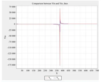
( )
cothth in
[image:10.595.181.456.244.308.2]y = −j
β
l (43) Withβ
is the propagation constant of the fundamental mode.Figure 4. Comparison between the calculated and theoretical input admittance for microstrip short-circuited line.
functions (trigonometric type), 94,000 TE and TM mode functions fmn (on source plan) and 68,900 TE and TM modes functions gpq (on circuit plan).
We observe that the two curves of the input impedance are very close with a relative error lower than 1%. This confirms the validity of our numerical approach and the perfect adaptation between source and circuit. In fact, among the parameters affecting the consistency of results precision of the fundamental mode taken as exci-tation source has the higher effect.
With X is the length l of the microstrip line.
5.2. Electromagnetic Characteristics of Microstrip Short-Circuited Line
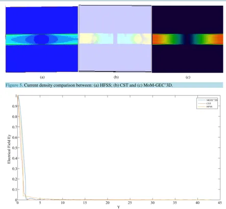
In this section, we present some electromagnetic characteristics (current density and electric field) for a micro-strip short-circuited line. We also compare the obtained results to the results found with two commercial soft-ware HFSS and CST.
Figure 5 illustrates shapes of the current density (HFSS, CST and MoM-GEC’3D). We observe that the three curves have the same variation of the current which satisfies the boundary conditions. This result is very consis-tent with excepted values for a short-circuited line for the specified dimensions.
Figure 6 and Figure 7 illustrate the shape of the electric field Ey along the propagation direction (oy). We
note that the electric field satisfies the boundary conditions. It is maximum at the source and presents a fast at-tenuation at source/line discontinuity. The result with the new approach MOM-GEC’3D contains small attenua-tion that tend to cancel due to the Gibbs effect. HFSS gives a less step attenuaattenua-tion at source/line discontinuity; whereas CST’s result has the best consistency
Figure 8 allows to verify the boundary conditions for the electric field Ex. The two figures obtained with CST
and MoM-GEC’3D confirms results alignment.
5.3. Electromagnetic Characteristics of Microstrip Open Circuit Line
(a) (b) (c)
Figure 5. Current density comparison between: (a) HFSS; (b) CST and (c) MoM-GEC’3D.
Figure 6. Electrical Field Ey comparison between: (a) HFSS; (b) CST and (c) MoM-GEC’3D: section along axis (ox).
[image:12.595.99.529.513.668.2](a) (b) (c)
Figure 7. Electrical Field Ey comparison between: (a) HFSS; (b) MoM-GEC’3D and (c) CST: 2D view.
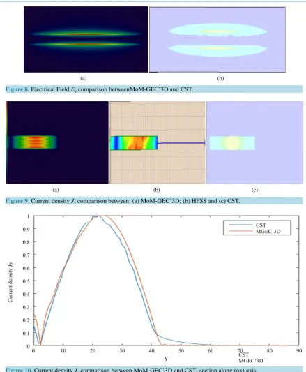
(a) (b)
Figure 8. Electrical Field Ex comparison betweenMoM-GEC’3D and CST.
[image:13.595.91.531.76.610.2](a) (b) (c)
Figure 9. Current density Jy comparison between: (a) MoM-GEC’3D; (b) HFSS and (c) CST.
Figure 10. Current density Jycomparison between MoM-GEC’3D and CST: section along (ox) axis.
wavelength, variations along (x) should not be relevant, which is the case of (a). Still CST have some important variation (at the center of the line). Moreover, a better attenuation (Figure 10) is remarkable with small Gibbs effect lead us to conclude that new approach gives more rigorous results.
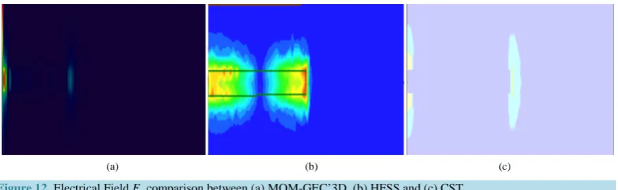
Figure 11 and Figure 12 illustrate that the electric field for the 3 simulation results verify the boundary con-ditions. We note also that the curve of MOM-GEC’3D contains small attenuation due to Gibbs effect. We may add an artificial additional term to compensate this effect and reduce numerical errors. Figure 12 gives even better confirmation of result validation as one can appreciate good attenuation of numerical results of Ey away
[image:13.595.101.526.360.600.2]Figure 11. Electrical Field Ey section along (oy): comparison between MOM-GEC’3D, CST and HFSS.
(a) (b) (c)
Figure 12. Electrical Field Ey comparison between (a) MOM-GEC’3D, (b) HFSS and (c) CST.
CST while HFSS gives a little more fuzzy results. All of three results still consistent with boundary conditions though.
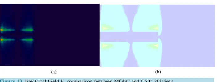
Similarly, the electric field component Ex verifies the boundary conditions for the result obtained with
MOM-GEC’3D and CST while CST, for this case, presents a better boundary conditions. This may be explained with the forced usage of (y) based test functions (in order to validate more generic approach) whereas line width is too small relatively to wavelength, so that Gibbs effect remains a little substantial (Figure 13).
The different simulations made for short circuit and open circuit demonstrates the accuracy of our new ap-proach. This was approved by the verification of the boundary conditions and comparison with two commercial simulation software HFSS and CST.
6. Conclusions
In this paper, we present a new formulation of the source method to characterize discontinuities in planar cir-cuits. A new definition of the excitation source is introduced to overcome the discontinuity problem at the source/circuit transition. We expose a general formulation of the source method, by determining the Input ad-mittance matrix of N-port discontinuity in a planar circuit. To validate our approach, we considered the case of a single vertical source. We detailed the determination of the various operators and rotational transformations re-quired to calculate the input impedance. In the last part of our work, we presented and interpreted some results in the case of a microstrip short-circuited line and microstrip open circuit line.
The numerical results obtained using this approach were compared to results obtained by both commercial software HFSS and CST. Our results show a concordance and consistency with those obtained using HFSS and CST, with even better results in most cases.
We also demonstrated that considering the fundamental mode of the access line to circuit as the excitation source gives us a perfect adaptation between the source and the circuit.
[image:14.595.89.540.259.398.2](a) (b)
Figure 13. Electrical Field Ex comparison between MGEC and CST: 2D view.
definition of the source in the integral analysis and the determination of admittance operators to link the elec-tromagnetic quantities of sources and magnitudes of the circuit, which are defined in vertical plans.
References
[1] Harrington (1961) Time Harmonic Electromagnetic Fields. Mac Graw Hill.
[2] Kunz, K. and Luebber, R. (1993) The Finite Difference Time Domain Method for Electromagnetics. CRC, Boca Ra-ton.
[3] Cherry, P.C. and Iscander, M.F. (1995) FDTD Analysis of High Frequency Electronic Interconnection Effects. IEEE Transactions on Microwave Theory Tech, 43, 2445-2451. http://dx.doi.org/10.1109/22.466178
[4] Ferrari, R.L. and Naidu, R.L. (1990) Finite-Element Modeling of High-Frequency Electromagnetic Problems with Ma-terial Discontinuities. IEEE Proc, 137, 313-320.
[5] Lee, J.F. and Sacks, Z. (1994) WETD—A Finite Elements Time Domain Approach for Solving Maxwell’s Equations.
IEEE Microwave Guided Wave Letters, 4, 11-13. http://dx.doi.org/10.1109/75.267679
[6] Hamdi, N., Aguili, T., Bouallegue, A. and Baudrand, H. (1998) A New Technique for the Analysis of Discontinuities in Microwave Planar Circuits. Progress in Electromagnetic Research, PIER, 21, 137-151.
http://dx.doi.org/10.2528/PIER98051101
[7] Aguili, T. (2000) Modélisation des composants S. H. F planairespar la méthode des circuits équivalentsgénéralisés. Ph.D. Thesis, National Engineering School of Tunis ENIT.
[8] Harrington, R.F. (1983) Field Computation by Moment Methods. MacMillan, New York.
[9] Ooms, S. and De Zutter, D. (1998) A New Iterative Diakoptics-Based Multilevel Moments Method for Planar Circuits.
IEEE Transactions on Microwave Theory and Techniques, 46, 288-291. http://dx.doi.org/10.1109/22.661716
[10] Aguili, T., Graya, K., Boualegue, A. and Baudrand, H. (1996) Application of a Source Method for Modeling Step Dis-continuities in Microstrip Circuit. IEE Proceedings—Microwaves, Antennas and Propagation, 143, 169-173.
http://dx.doi.org/10.1049/ip-map:19960224
[11] Hamdi, N., Aguli, T. and Boualegue, A. (1998) Considération des sources dans la caractérisation des discontinuities dans les guides d’ondescoplanaires. 6ème colloque Maghrébinsur les Modèles Numériques de l’iIngénieur, Tunis, 24-26 November 1998.
[12] Hamdi, N., Aguili, T. and Boualegue, A. (1998) Caractérisation des discontinuitésdans les circuits planaires mi-cro-ondes avec une nouvelle technique intégrale. Mediterranean Conference on Electronics and Automatic Control, Marrakech Maroc, 17-19 September 1998.
[13] Hamdi, N. (1999) Analyse des Discontinuitésdans les circuits planaires par une Nouvelle Formulation de la méthode des Sources. PhD Thesis, National Engineering School of Tunis, ENIT, Tunis.
[14] El Gouzi, M.E.A. and Boussouis, M. (2010) Hybrid Method for Analyse Discontinuities in Shielded Microstrip. Inter-national Journal of Engineering Science and Technology, 2, 3326-3334.
[15] Pujol, S., Baudrand, H. and Hanna, F. (1993) A Complete Description of a Source Type Method for Modelling Planar Structures. Annals of Telecommunications, 48, 459-470.
[16] Graya, K., Aguili, T., Boualegue, A. and Boudrand, H. (1999) Characterization of Planar Passive Circuits Using Source Method in Conjunction with Three Different Sets of Trial Functions. IEE Proceeding-Microwaves, Antennas and Propagation, 146, 209-213. http://dx.doi.org/10.1049/ip-map:19990628
http://dx.doi.org/10.1109/icm.1998.825586
[18] Graya, K., Aguili, T. and Boualegue, A. (1999) Etude de discontinuitésplanaires en microruban par uneméthode de source avec différents types d’excitations, Journéessur les télécommunications, Tunisia, 29-31 January 1999.
[19] Golio, M. and Golio, J. (2007) RF and Microwave Passive and Active Technologies. RF and Microwave Handbook, Second Edition,CRC Press,Boca Raton. http://dx.doi.org/10.1201/9781420006728
[20] Hitendra, K., Malik, A. and Singh, K. (2009) Engineering Physics.
[21] El Gouzi (2015) Modélisation des discontinuitesuni-axialesdans les circuits planairespar la méthode des moments. PhD Thesis, Université Abdelmalek Essaadi, Tétouan.
[22] Ourabia, M. (2014) Modelling and Characterization of Planar Components. Advanced Materials Research, 1025-1026, 1055-1061. http://dx.doi.org/10.4028/www.scientific.net/amr.1025-1026.1055
[23] Lea, D. (1997) Concurrent Programming in Java. Addison Wesley Pub.,Boston.
[24] Weems, C.C., Weaver, G.E. and Dropsho, S.G. (1994) Linguistic Support for Heterogeneous Parallel Processing: A Survey and an Approach. Proceedings of the Heterogeneous Computing Workshop, Cancun, 26 April 1994, 81-88.
[25] Weems, C. (1998) Heterogeneous Programming with Java: Gourmet Blend or Just a Hill of Beans? Proceedings of the
7th Heterogeneous Computing Workshop, Orlando, 30 March 1998, 173-182.
[26] Salah, T.B. (2009) Etude des structures invariantes par échelles par uneméthodeintégrale multi modalecombinée à la méthode de normalization. PhD Thesis, National Engineering School of Tunis, ENIT, Tunis.