EMULEX
FEATURES
o
Supports ANSIX3.131 SCSI Standardo
Supports synchronous data transfers of 5 MB/sec Programmable synchronous transfer period - Programmable synchronous offsets up to15 bytes
o
Buffer controller interface for I/O and fast DMAo
Contains control logic for differential transceiverso
Up to 12MB/sec DMA burst transfer rateo
Interfaces to 8-bit microprocessor data bus with no support logico
On-chip single-ended SCSI transceivers (48-mA drivers)*
ESP200 refers to ESPIOOA as well, except as noted.EMULEX l\flCRO DEVICES
SCSICIllP
ESP200/100A
*
o
Functions as initiator or targeto
Utilizes pipelined command structureo
16-byte data FIFO between the DMA and SCSI channelso
Clock rates up to 25 MHzo
Low power requirementso
SCSI sequences implemented without microproces-sor interventionSelection sequence from arbitration through command
Reselection sequence from arbitration through message
Bus-initiated selection through received command
Command complete sequences Terminate and disconnect sequences
r---~
<J--T
DB Bus
I
~
I
I
r--<J-I
~I
~
I
I
H>
I
I
J FIFO IL----[>-
L-Command
]
....Transfer Count I Transfer Counter
J
~I
...
-=
t
s
:It:\
rtJ
" SelectlReselect
-->
rtJ:I BusID :I
~ ~
;.. ;..
Ql SelectlReselect
~
~
1]-->
~
...
,.Timeout Interrupt
rtJ
.6h - - .6h
Ql
~
1]-->
~~ .... Sequencers Status
Sync Period
-->
,Sync Offset!
~
~
Sequence Step1]-->
Sync Assert! Sync De-assert
,. Clock Conversion
I
" Configuration ,.
I
f--- > Test
I
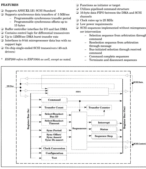
[image:1.624.49.562.132.724.2]L ____________________________
~Figure 1. ESP200 Block Diagram
Mode 2/3
SCSI Data
SCSI Control
ge
EMULEX ESP200 / lOOA
o
Microprocessor interrupted only when service is requiredDisconnect or bus reset
Selectionlreselection sequence complete Target Mode command complete or ATN detected
Initiator Mode complete or phase change detected
PRODUCT DESCRIPTION
The Emulex SCSI Processor (ESP200) chip is a VLSI device which implements the detailed protocol of the SCSI Bus Standard. The ESP200 chip operates in both the Initiator and Target modes and can therefore be used in both host adapter and peripheral applica-tion. The chip performs such functions as bus arbitra-tion, selection of a target, or reselection of an initiator. The ESP200 handles message, command, status and data transfers between the SCSI Bus and its internal FIFO or a buffer memory. Figure 1 shows the internal architecture of the ESP200. The chip maximizes protocol efficiency by utilizing a first-in, first-out command pipeline and combination commands to minimize host intervention.
The ESP200 has been optimized for interaction with the controller processor. Common SCSI bus sequences that would typically require significant amounts of processing and interaction have been reduced to single commands. The commands are listed in Table 1. SYSTEM ORGANIZATION
The ESP200 chip provides a controller with a complete SCSI interface. The other major chips in the circuit include the Emulex Merged Architecture Controller (MAC) and a microprocessor.
The MAC chip controls data movement in and out of the buffer memory. It supports up to four DMA channels with a total throughput rate up to 4MB/sec and provides format control for a wide spectrum of 14-, -8, 5.25-, and 3.5-inch disk drives.
The 8031 microprocessor coordinates the interaction of the VLSI devices on the board. It also implements high level SCSI protocol, such as the message system, SCSI pointers, and command set.
Page 2
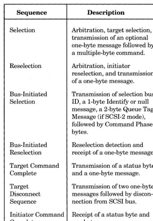
Sequence Description
Selection Arbitration, target selection, transmission of an optional one-byte message followed by a multiple-byte command. Reselection Arbitration, initiator
reselection, and transmission of a one-byte message. Bus-Initiated Transmission of selection bus Selection ID, a I-byte IdentifY or null
message, a 2-byte Queue Tag Message (if SCSI-2 mode), followed by Command Phase bytes.
[image:2.623.308.557.69.427.2]Bus-Initiated Reselection detection and Reselection receipt of a one-byte message. Target Command Transmission of a status byte Complete and a one-byte message. Target Transmission oftwo one-byte Disconnect messages followed by discon-Sequence nection from SCSI bus. Initiator Command Receipt of a status byte and Complete one-byte message.
Table 1. ESP200 Single SCSI Commands
REGISTERS
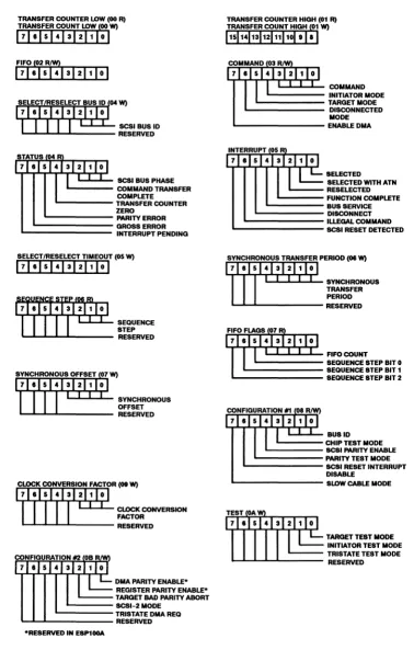
The ESP200 registers are used to configure, command, monitor and pass data to the chip. These registers are shown in Figure 2. The Command Register is an 8-bit read/write register used to give commands to the ESP200. The register is double ranked, enabling the microprocessor to stack one level of command to the ESP200.
INTERFACES
The ESP200 has two separate interfaces: the buffer data bus and the SCSI Bus. The buffer data interface is used for strobe, DMA request, DMA acknowledge and microprocessor interrupt signals. For DMA operations, the buffer controller manages access timing and generates all buffer memory addresses. The SCSI Bus signals have separate input and output pins. All are 8-bit busses. The SCSI interface can be configured for operation in either single-ended or
ESP200/100A
FIFO(02Rr;
I
71 .1
5}I
31 211
I
0
I
~~~il~jl~~~
SCSI BUS IDL... ... _ _ _ _ RESERVED
'r'rIII1:J::J::~
SCSI BUS PHASE ... - - - COMMAND TRANSFERCOMPLETE ... - - - - TRANSFER COUNTER
ZERO ' - - - PARITY ERROR ... - - - GROSS ERROR ' - - - INTERRUPT PENDING
SEQUENCE STEP RESERVED
L... ... L.- SYNCHRONOUS OFFSET
L... ... _ _ _ _ _ RESERVED
DMA PARITY ENABLE* REGISTER PARITY ENABLE* ' - - - - TARGET BAD PARITY ABORT ' - - - - SCSI-2 MODE
' - - - TRISTATE DMA REQ
L... ... _ _ _ _ _ RESERVED -RESERVED IN ESP100A
~~~~ic~JCJC~
COMMAND ' - - - INITIATOR MODEL~=====: TARGET MODE DISCONNECTED
MODE
L-_ _ _ _ _ _ _ ENABLE DMA
SELECTED SELECTED WITH ATN ' - - - - RESELECTED ... - - - FUNCTION COMPLETE ' - - - BUS SERVICE
L.. _ _ _ _ _ DISCONNECT ' - - - ILLEQALCOMMAND ' - - - SCSI RESET DETECTED SYNCHRONOUS TRANSFER PERIOD (01 W)
171·1514131211101
III ' , , "
SYNCHRONOUS TRANSFER PERIODL-... _ _ _ _ _ RESERVED
.,..,..,.a;::3:~J::J::~
FIFO COUNT ' - - - SEQUENCE STEP BIT 0L-_ _ _ _ _ _ SEQUENCE STEP BIT 1
L... _ _ _ _ _ _ _ SEQUENCE STEP BIT 2
11111,:3:3:"
BUSID' - - - CHIP TEST MODE
L.. _ _ _ _ SCSI PARITY ENABLE ' - - - PARITY TEST MODE ' - - - SCSI RESET INTERRUPT
DISABLE ' - - - SLDWCABLE MODE
TARGET TEST MODE INITIATOR TEST MODE ' - - - - TRISTATE TEST MODE
[image:3.613.115.493.96.689.2]L..L-JL-JL...JL..-_ _ _ RESERVED
Figure 2. ESP200 Register Summary
9E
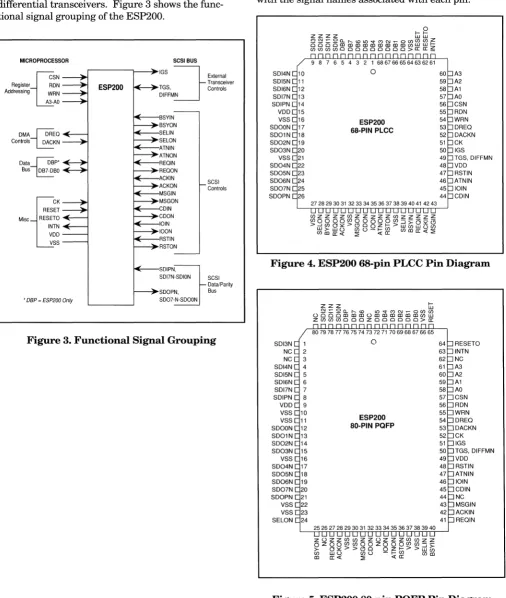
EMULEX ESP200/100Adifferential mode. In the single-ended mode, the SDII SDO lines interface directly with the SCSI Bus. In differential mode, the SDI bus becomes bidirectional and the SDO bus controls the direction of the external differential transceivers. Figure 3 shows the func-tional signal grouping of the ESP200.
MICROPROCESSOR
U
SNRegister RDN Addressing WRN A3-AO DMA.-JDREQ
Controls~KN
DataSDsP' Bus ~BO
CK RESET Mise RESETO INTN VDD VSS
• DBP = ESP200 Only
ESP200
SCSI BUS External Transceiver IGS
J
TGS, Conlrols DIFFMN BSYIN BSYON ELiN SELON ATNIN ATNON REQIN REQON ACKIN ACKON MSGIN MSGON DIN CDON lOIN lOON STIN RSTON SDlPN, SCSI Controls [image:4.613.50.556.125.723.2]SDI7N-SDION SCSI Data/Parity SDOPN, Bus SD07-N-SDOON
Figure 3. Functional Signal Grouping
Page 4
PIN DESCRIPTIONS
Figures 4 and 5 illustrate the ESP200 pins for both the PLCC 68-pin and the PQFP 80-pin models, together with the signal names associated with each pin.
SDI4N SDI5N SDI6N SDI7N SDIPN VDD VSS SDODN SD01N SD02N SD03N VSS SD04N SD05N SD06N SD07N SDOPN ESP200 S8-PIN PLCC
A3 A2 A1 AD CSN RDN WRN DREO DACKN CK IGS TGS, DIFFMN
VDD
RSTIN ATNIN lOIN CDIN
Figure 4. ESP200 68-pin PLCC Pin Diagram
SDI3N NC NC SDI4N SDI5N SDI6N SDI7N SDIPN VDD VSS VSS SDOON SD01N SD02N SD03N VSS SD04N SD05N SD06N SD07N SDOPN VSS VSS SELON
ZZZ
f-~:::!::9a..",<o LO.q-M(\J.,...O(/)~
OOOOOlOlOlOOlOlOlOlOlOlC/lW ZC/lC/lC/looozoooooo>a: OON~n~~Nnnnrooooo~oo~ o ESP200 80-PIN PQFP RESETO INTN NC A3 A2 A1 AD CSN RDN WRN DREO DACKN CK IGS TGS, DIFFMN
[image:4.613.286.544.156.705.2]VDD RSTIN ATNIN lOIN CDIN NC MSGIN ACKIN REOIN
[image:4.613.312.555.419.701.2]ESP200/ lOOA
9E
EMULEXACTIMING
The following figures and table values are illustrative ofthe ESP200 chip timing characteristics. For more information, see the ESP200/100A Application Manual, VLSI51002-00.
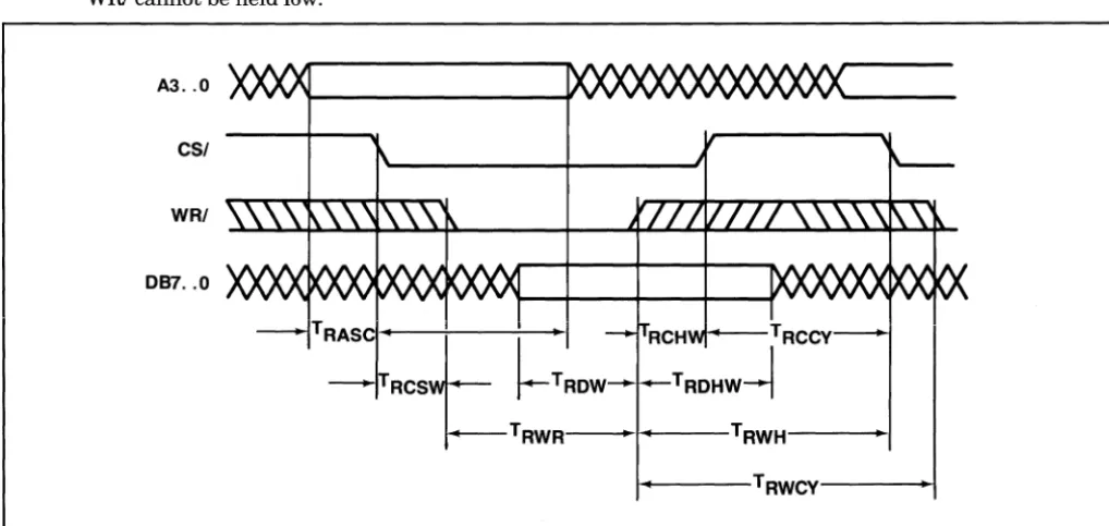
REGISTER INTERFACE Register Write (in ns)
For the following register write operations, note that ACKI must be inactive during all register I/O, and CS/ must make a high to low transition to capture a new register address. Reserved registers should not be ac-cessed.
Symbol Description Minimum Maximum
TRASC Address Setup to CS/ 0
TRCSWI CS/ Setup to WRI 0
TRWR WRI Pulse Width 40
TRDW Data Setup to WRI 11
TRAHC Address Hold from CS/ 50
TRDHW Data Hold from WRI 0
TRCHWl,2 WRI High to CS/ High 0/50
TRWCY WRI High to WRI Low 60
TRWH WRI High to CS/ Low 60
TRCCyl CS/ High to CS/ Low 40
Notes:
1. WRI edges may precede or follow CS/ edges. Recommended values are TRCSW ;:::: 0 and TRCHW ;:::: 0, unless Note 2. below applies. IfWRI is held low, the data setup to CS/ high is 25ns minimum, the data hold from CS/ high is 60ns minimum, and TRCCY is 60ns minimum.
2. ESP200 only: TRCHW must be;:::: 50ns if writing to the FIFO register and the DMA Parity Enable bit does not equal the Register Parity Enable bit (Configuration #2 Register bits 0,1). Under this condition, WRI cannot be held low.
A3 .. 0
CSI
WRI
087 .. 0
---~~----TRWH----~~I
[image:5.618.57.566.470.711.2]~---TRWCY---~
Figure 6. Register Write
9E
EMULEX ESP200/ 100A
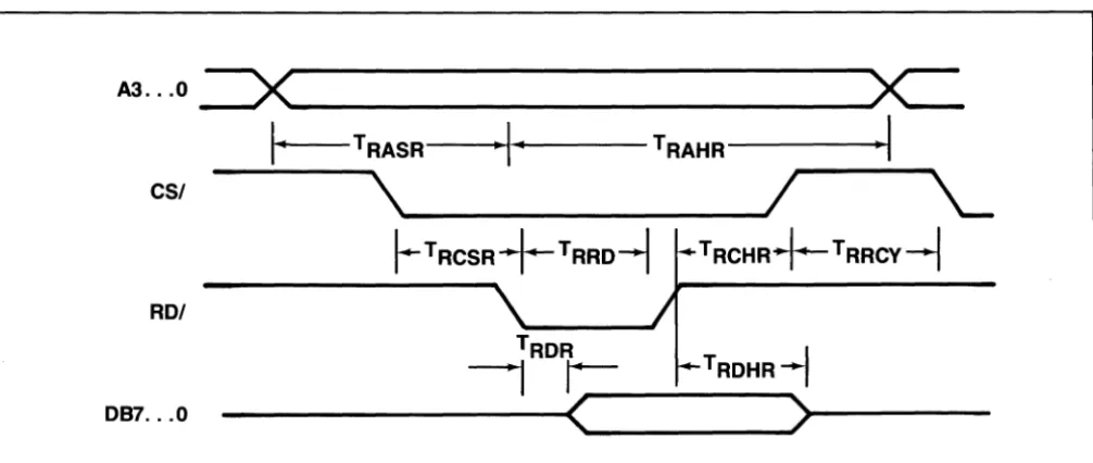
Register Read (in ns)
For the following register read operations, note that ACKI must be inactive during all register 110, and CSI must make a high to low transition to capture a new register address. Reserved registers should not be accessed.
Symbol Description Minimum Maximum
TRASC Address Setup to CSI 0
TRCSR 1 CSI Setup to RDI 20
TRRD RDI Pulse Width 50
TRDR2 RD/toData 50
TRDC2 CS/to Data 70
TRAHC Address Hold from CSI 50
TRDHR Data Release Time 2 40
TRCHRI RDI High to CSI High 2
TRRCY CSI High to CSI Low 40
Notes:
1. RDI edges may precede or follow CSI edges. Recommended values are TRCSR > TRDC - TRDR, and TRCHR:> TRDHR. IfRDI is held low, the time from CSI low to stable data is TRDC, and the data release time from CSI high is TRDHR.
2. TRDC and TRDR must both be satisfied.
A3 ... 0
==>< _____________
>C.
~TRASR____1~.---TRAHR---~·1
CSI \ ' - - -_ _ _ _ _ _ _ _ _ _
1
ROI
_ _ _
J
TROR
I
I
r=
f+-TROHR~
[image:6.618.57.560.378.591.2]---~<---)~---087 ... 0
Figure 7. Register Read
ESP200/ lOOA
9E
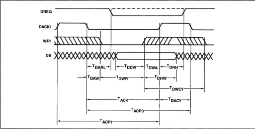
EMULEXDMA INTERFACE DMA Write (in ns)
For the following DMA write operations, note that CS/ must be inactive during all DMA accesses, and DACKI
must toggle once for each write access. DREQ remains active as long as the FIFO is not full and the Transfer Counter is not zero.
Symbol Description Minimum Maximum
TDARL DACKI Low to DREQ Low (negation pending) 0 38
TDAWI DACKI Low to WRI Low 0
TDWR WRI Pulse Width 40
TDDW Data Setup to WRI 11
TDWAI WRI High to DACKI High 0
TDHW Data Hold from WRI 0
TDACyl DACKI High to DACKI Low 12
TDRH DACKI High to DREQ High (assertion pending) 50
TDWCY WRI High to WRI Low 40
TACK DACKI Pulse Width 50
TACPO DACKI Period (Low to High)(sync SCSI transfer) 83.33 TACP1 DACKI Period (High to High) TCS + 35ns
-TDACYand 2TCP Notes:
1. WRI edges may precede or follow DACKI edges. Recommended values are TDA W ;::: 0 and TDWA ;:::
o.
If WRI is held low, the data setup to DACKI high is 15ns minimum, the data hold from DACKI high is 15ns minimum, and TDACY is 40ns minimum.DREQ
DACKI
DB
---
...- - -
-
- - - -
-
-
--,,---TOWA _ TORH
--~-TDHW-l
~-~I-_TDWCY~~~
~---TACK---~'~TDACV
t - - - -T ACPO,---7---~
[image:7.615.58.566.449.705.2]I - - - T ACP1---.1
9E
EMULEX ESP200/100ADMA Read (in ns)
For the following DMA read operations, note that CSI must be inactive during all DMA accesses, and DACKI
must toggle once for each read access. DREQ remains active as long as the FIFO has data to be read and the Transfer Counter is not zero.
Symbol Description Minimum Maximum
TDARL DACKI Low to DREQ Low (negation pending) 38
TDARI DACKI Low to RDI Low 0
TDRD RDI Pul~ Width TDDR
TDDR2 RD/toData 41
TDRAI RDI High to DACKI High 0
TDHR Data Release Time 2 40
TDACY DACKI High to DACKI Low 12
TDRH DACKI High to DREQ High (assertion pending) 50
TDDALI DACKI Low to Data 41
TDDAH Previous DACKI High to Data 60
TACK DACKI Pulse Width 50
TACPO DACKI Period (Low to Low) 83.33
TACP1 DACKI Period (High to High)(sync SCSI transfer) TCS + 35ns -TDACYand
2TCP Notes:
1. RDI edges may precede or follow DACKI edges. Recommended values are TDAR ;::: 0, and TDRA ;::: O. If
RDI is held low, the time from DACKllow to stable data is TDDAL, and the data release time is TDHR. 2. TDDR, TDDAL, and TDDAH must all be satisfied.
DREQ
DACKI
RDI
DB
PageS
---
...---
"..---t - - _T
DDAL--"-t----~TDDAH----~~I
t---TACK---~--TDACY-1 4 - - - T ACPO'---... - - - . . - j
[image:8.613.50.556.387.704.2]~
___________ T A C P 1 - - - . 1 Figure 9. DMA ReadESP200/ 100A
3.e
EMULEXSCSI INTERFACE
Target Asynchronous Data In Phase (in ns)
Symbol Description Minimum Maximum
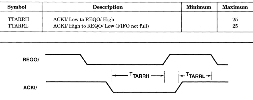
TTAXDR Data to REQOI 55
TTAXRH ACKII Low to REQOI High 25
TTAXAD ACKII Low to Data (FIFO bottom full) 40
TTAXRL ACKII High to REQOI Low (data already set up) 25
SOOt
~~
__~
______________________)(~
______ _---.IT TAXOR'-- b
I
-I
1-
~---TTAXAO---~~~-REQOt
ACKII
TTAXRH~ r:TTAXRL~
[image:9.618.55.565.139.392.2]\ ______
1
Figure 10. Target Asynchronous Data In Phase
Target Asynchronous Data Out Phase (in ns)
Symbol Description Minimum Maximum
TTARRH ACKII Low to REQOI High 25
TTARRL ACKII High to REQOI Low (FIFO not full) 25
REQO/
\'-_ _ _
----J/
I-
T TARRH-I
I:
T TARRL--l\ _ _ _
---11
ACKI/
[image:9.618.58.564.473.673.2]9E
EMULEX ESP200/100AInitiator Asynchronous Data In Phase (in ns)
Symbol Description Minimum Maximum
TIARAH REQII High to ACKO/ High
25
TIARAL REQII Low to ACKO/ Low (FIFO not full)
25
ACKOI
\~
_ _ _
---JI
I -
TIARAH--jI-
TIARAL-jREQII
____
._1
\'---Figure 12. Initiator Asynchronous Data In Phase
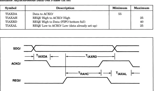
Initiator Asynchronous Data Out Phase (in ns)
Symbol Description Minimum Maximum
TIAXDA Data to ACKO/
55
TIAXAH REQII High to ACKO/ High
25
TIAXRD REQII High to Data (FIFO bottom full) 40
TIAXAL REQII Low to ACKO/ Low (data already set up)
25
SOOI
=x
X
-I
TIAXOAr-
TIAXRO~
I
ACKOI
TRAHC
~1--1
TIAXAL~
[image:10.617.50.558.102.304.2]REQII
/
\
Figure 13. Initiator Asynchronous Data Out Phase
[image:10.617.48.562.361.666.2]ESP200/ 100A
9E
EMULEX Synchronous Transfer (in ns)Symbol Description Minimum Maximum
TSXD Data from CK High 40
TSXDR Data to REQO/ Low 55
TSXDA Data to ACKO/ Low 55
TSXRL REQO/ Low from CK High 35
TSXRH REQO/ High from CK Low 35
TSXAL ACKO/ Low from CK High 35
TSXAH ACKO/ High from CK Low 35
TSAST Assertion Period 90
TSNEG Negation Period 90
CK
I--
TSX0-1 SOOITSXRL--j ~TSXRH1 _TSXRL-j REQOI
- - TSXOR --'\
ACKOI
~
TSXAL-j TSXAH-1
TSXALjTSXOA
-!--
T S A S T - t - [image:11.615.55.565.94.494.2]3E
EMULEX ESP200 / lOOA
Emulex is a registered trademark of Emulex Corporation
Emulex Corporation, 3545 Harbor Blvd., Costa Mesa, CA 92626, (800) EMULEX-3 or (714) 662-5600 in California North America Offices: Anaheim, CA (714) 385-1685; San Jose, CA (408) 452-4777;
Rosewell, GA (404) 587-3610; Burlington, MA (617) 229-8880; Saddle Brook, NJ (201) 368-9400; Houston, TX (713) 981-6824; Reston, VA (703) 264-0670; Schaumburg, IL (708) 605-0888
International Offices: Workingham (44) 71-4772929; Munich (49) 89-3608020;
Sydney (02) 417-8585; Paris (33) 134-65-9191; Milan (39) 39-639261; Toronto (416) 673-1211; Hong Kong (852) 529-2705
Emulex Micro Devices Sales Representatives: Montgomery Marketing (919) 467-6319 - Alabama, Georgia, Florida Pan Handle, No. Carolina, South Carolina, Tennessee; ProMerge, Sales (408) 453-5544 - No. California, No. Nevada;
Sales Engineering Concepts (305) 426-4601 - Florida, Puerto Rico; West Associates (214) 680-2800 - Mississippi, Oklahoma, Texas; Advanced Tech Sales, Inc. (508) 664-0888 - Massachusetts, Connecticut, Vermont,
New Hampshire, Maine, Rhode Island; Oasis Sales Corporation (708) 680-2800 - No. Illinois, Wisconsin, Iowa, North Dakota, South Dakota, Minnesota