http://www.sciencepublishinggroup.com/j/ajcst doi: 10.11648/j.ajcst.20180103.11
ISSN: 2640-0111 (Print); ISSN: 2640-012X (Online)
Computer Aided Design-Based Band Diagram Development
for High Performance Solar Cells
Hnin Lai Lai Aye
Department of Electronic Engineering, Yangon Technological University, Yangon, Republic of the Union of Myanmar
Email address:
To cite this article:
Hnin Lai Lai Aye. Computer Aided Design-Based Band Diagram Development for High Performance Solar Cells. American Journal of Computer Science and Technology. Vol. 1, No. 3, 2018, pp. 55-62. doi: 10.11648/j.ajcst.20180103.11
Received: November 3, 2018; Accepted: November 15, 2018; Published: December 26, 2018
Abstract:
There are essentially different forms of solar cell panels that are used in either for domestic uses or industrial purposes depending on the semiconductor materials. Actually, there are enormous amount of semiconductor and these various types can be combined or adjust the composition of the material can form the new compound of semiconductor. In this paper, the basic concepts of semiconductors that are used for in all aspects of material science and optical devices are firstly described with both theoretical and mathematical approaches. The main objective of this research is to design and analyse the band diagram design of semiconductor materials which are used for high performance solar cells. This paper describes the fundamental theory of semiconductors, the properties analysis and band gap design of materials for solar cells. Firstly, as the physical properties play a vital role in semiconductor measurements, the properties such as effective mass of majority and minority carriers, the dielectric constants and energy band gaps are calculated. Depending on the specified semiconductor material, the required parameters and the mathematical calculation are performed based on the existing equations. Secondly, the optical properties and the characteristics curves of semiconductor materials are discussed. Numerical values of each parameter which are included in analysis are defined in order to achieve the current-voltage characteristic for specific solar cell and then these resultant values are predicted for the performance of solar cells. Finally, the energy band diagram and efficiency of semiconductor solar cells are presented. Therefore, this research is focused in analyzing the useful properties of semiconductor materials for solar cells. The computerized analyses have also mentioned in this paper.Keywords:
Computer Aided Design, Semiconductor Materials, Solar Cells, MATLAB, Computer Technology1. Introduction
This research focuses on energy band diagram design and other important properties of semiconductor materials which can be useful for solar cells especially aiming for obtaining high performance. Basically, semiconductors are applied in the fabrication of electronic devices so they play an important role in our daily life. Semiconductor materials are the foundation of modern day electronics such as radio, computers and mobile phones. They are used in the manufacturing of electrical components and used in electronic devices such as transistors and diodes. Moreover, semiconductors are the most essential and demanding items in current energy resources. They are performed as different roles in various applications such as solar cells, light emitting diodes (LEDs), laser diodes, regulators, switching systems and so on.
Semiconductors are a group of materials possessing electrical conductivity value between that of conductors, like copper, gold, etc. and insulators such as glass and rubber. Semiconductors have special property which behavior is opposite to that of metals. This means that the resistance of semiconductors decreases as the temperature increases. Semiconductor devices can display some ranges of essential properties such as passing current more easily in one direction rather than the other materials, showing variable resistance, and sensitivity to light or heat. Among various elements and compounds, some of them have semiconductive properties, including:
and germanium are used effectively because they have 4 valence electrons in their outermost shell which gives them the ability to gain or lose electrons equally at the same time,
2. binary compounds, particularly between elements in group 13 and 15, such as gallium arsenide, elements from group 12 and 16, group 14 and 16, and between different group 14 elements,
3. certain ternary compounds, oxides and alloys and 4. organic semiconductors that are made of organic
compounds.
Most of the recent researches have been based on two general classifications of semiconductors. The first one is elemental semiconductor materials, found in group 14 of the periodic table, which are the most abundant and easiest to fabricate. Another one is compound semiconductor materials, most of which are formed from special combinations of group 13 and group 15 elements and also a few of the semiconductor materials that can be formed from combinations of group 12 and group 16 elements.
Typically, semiconductor materials can be classified into mainly two categories known as intrinsic semiconductors and extrinsic semiconductors. An intrinsic semiconductor material is very pure and possesses poor conductivity. It is a single element not mixed with anything else. On the other hand, extrinsic is a semiconductor material to which small amounts of impurities are added in a process called doping which cause changes in the conductivity of the material. The doping process produces two groups of semiconductors which include the negative charge conductor known as n-type and the positive charge conductor known as p-n-type. The materials selected to be added to an intrinsic depend on the atomic properties of both the material being added and the material to be doped [1].
As the subtle increase in world’s population per year, the enormous amount of energy consumption cannot cover up for all people in every region of the world. Not only the natural resources but also the artificial energy resources, especially, renewable energy are needed to manufacture and utilize for long-term use. Solar cells are also one of the renewable energy resources and nowadays, they are widely used in most countries. Moreover, the biggest industry like farming which needs manpower and energy resources such as coal and fossil fuel generators therefore, the greater environmental benefits will give in having solar panels to supply electric power.
Although a great number of semiconductor materials are used in solar cells, the material which can conduct the greater efficiency of solar cells are still investigated and analyzed. The low-cost, the high performance and the simple way of fabrication and usefulness are mostly demanded in industry. In addition, semiconductor materials that match the properties of solar cells are required to analyze. This research emphasizes on the calculation of the band diagram, the voltage-current characteristics and the efficiency over the material composition using the theoretical concepts and mathematical equations.
The main process of this entire paper is to analyse on band
structure design of semiconductor materials for high performance solar cells using theoretical and mathematical approaches. First and foremost, the fundamental properties and some important parameters that will perform for all related equations will be described in details. The theories of p-n junction and the related equations to draw the band diagram of semiconductor material will be presented. In addition, this paper includes the mathematical calculation that is required to obtain the characteristics of the individual semiconductor material. Secondly, the voltage current characteristics and efficiencies for different mole fractions of semiconductor is calculated and analysed. Finally, other optical properties that are associated with the basic concepts of semiconductors will be included in this paper. Therefore, the fundamental needs for high performance solar cells and some essential properties are presented for this paper development [2-7].
2. Energy Bands
In this section, energy band diagram of AlGaInP heterojunction material and its properties are expressed. Mathematical descriptions are briefly explained and test results of the material are shown. The equilibrium condition of p-n junction diagram, the voltage-current characteristics of material, and calculation results of the high efficiency solar cells are described in this section [8-13].
2.1. GaAs Material
Before the results of AlGaInP heterojunction material are presented, the main reason of analyzing the GaAs material is that the AlGaInP material which will be focused for this thesis is similar in lattice structure and the properties of GaAs material are almost the same with that of AlGaInP material. Gallium Arsenide (GaAs) is an important semiconductor material for high-cost, high efficiency solar cells and is used for single-crystalline thin film solar cells and for multi-junction solar cells. Currently, GaAs based devices hold the world record for the highest-efficiency single-junction solar cell at 28.8%. The compound AlGaAs is also used for not only in solar cells but also other various researches like quantum wells and in the detection of X-rays.
2.2. Energy Band Diagram of GaAs Heterojunction Material
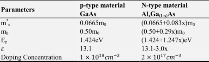
In GaAs heterojunction material, p-type material is assumed to use GaAs material and AlxGa(1-x)As compound
Table 1. Parameters For Calculating Energy Band Diagram of GaAs Heterojunction.
Parameters p-type material GaAs
N-type material AlxGa(1-x)As
m*e 0.0665m0 (0.0665+0.083x)m0
mh 0.50m0 (0.50+0.29x)m0
Eg 1.424eV (1.424+1.247x)eV
13.1 13.1-3.0x
Doping Concentration 1 10 2 10
As the mole fraction of N-type material can be changed from x=0 to 1. In this study, assume x=0.3 and because of Al0.3Ga0.7As heterojunction is applied to increase Voc, and
lead to higher fill factor (FF) and thereby higher power conversion efficiency. As the Al composition (x) of AlxGa (1-x)As exceeds 0.45, the band gap changes from direct to
indirect, unsuitable as the absorbing layer. Moreover, for x=0.35–0.45, the carriers in the indirect band (X-valley) are more dominant than those in the direct band. Therefore, Al0.3Ga0.7As is chosen for the heterojunction in this
calculation. By substituting x=0.3, the parameters of N-type material can be obtained.
For the band edge discontinuities, the change of energy in conduction band, valance band and energy band gap can be derived. In GaAs- Al0.3Ga0.7As system,
∆Eg = EgN – Egp (1)
∆Ec = 0.67 ∆Eg (2)
∆Ev = 0.33 ∆Eg (3)
In addition, the acceptor and donor concentrations for both p and N sides can be processed and also the differences between the Fermi level and the two energy bands have been described in Section 3. After that, the carrier concentrations of the conduction band and the valance band are calculated. The p side and N side parameters are presented individually.
For p-GaAs region,
* = 0.0665m0, * = 0.50m0
Egp = 1.424eV, = 13.1
= 2 ∗ = 2.51 10 ( . ""# $
$
= 4.30 10
% = 2 & ∗
= 2.51 10 ( .# $
$ =
8.87 10
p = '= Nv exp (()* +*) = 1 10
, - .% ≅ -012 ln 5) = ≅ -012 ln 565) = 56.4 meV
For N- Al0.3Ga0.7As region,
* = (0.0665 + 0.083x)m0 = 0.0914 m0
* =(0.50+0.29x) m0 = 0.587 m0
EgN = (1.424+1.247x)eV = 1.798 eV, 7 = (13.1-3.0x) =
12.2
= 2 ∗ = 2.51 10 ( . 8 $
$
= 6.94 10
% = 2 & ∗
= 2.51 10 ( .# $
$
= 1.13 10
N = 9= Nc exp (
+: (;:
) = 2 10
.5- ,5≅ -012 ln 5)5 = ≅ -012 ln 55)< = 32.2 meV
The band edge discontinuities are
∆Eg = ∆EgN - ∆Egp = 0.374 eV
∆Ec = 0.67 ∆Eg = 250.6 meV , ∆Ev = 0.33 ∆Eg = 123.4
meV
The contact potential and depletion width of p-N junction need to be calculated in order to plot the energy band diagram. For these two parameters, the fundamentals and the related equations are described.
V0 = Egp+∆Ec-(Fp-Evp)-(EcN -FN)/q = (1424 + 250.6 - 56.4 -
32.2) mV V0 = 1586 mV
The depletion widths from p-side and N-side are
x?@ AEFGFHBCD$FHIJC JKFG
L ND
= [ . . #8 MNO .# "
." MNP NQ NR NRINS.N
N . NQL 2 10
= 0.019Um
Figure 1. Energy Band Diagram of p-GaAs/N- Al0:3Ga0:7 As
Heterojunction.
V5@5W*< ' = 0.095 Um
The total depletion width of p-n junction at equilibrium condition is
VX@ V + V5 = 0.114 Um
2.3. Efficiency
The efficiency of GaAs heterojunction material has to be computed in order to analyze how much percentage of the photon energy are absorbed by the solar cell. The doping concentrations of the electrons and holes of the heterojunction material are designed as the same with the calculation of that of the energy band diagram.
For p-GaAs region,
Un = 8500 cm2/V.s, Up = 400 cm2/V.s
Dn = Y Un = 0.0259 8500 = 220 cm2/s
Dp = Y Up = 0.0259 400 = 10 cm2/s
@ 4.30 10 , % = 8.87 10
For N- Al0.3Ga0.7As region,
Un = 2300 cm2/V.s, Up = 145 cm2/V.s
Dn = Y Un = 0.0259 2300 = 60 cm2/s
Dp = Y Up = 0.0259 145 = 4 cm 2
/s
@6.94 10 , % = 1.13 10
The intrinsic carrier concentrations for both materials are
ni (For p-type) = Nc Nv exp ( - (Z )
=4.30 1017 8.87 1018 exp ( ." .8 8M[ ) ni (For p-type) = 2.1 106cm-3
ni (For N-type) = Nc Nv exp ( - (Z )
=6.94 1017 1.13 1018 exp ( ." . M[ ) ni (For N-type) = 2.2 103cm-3
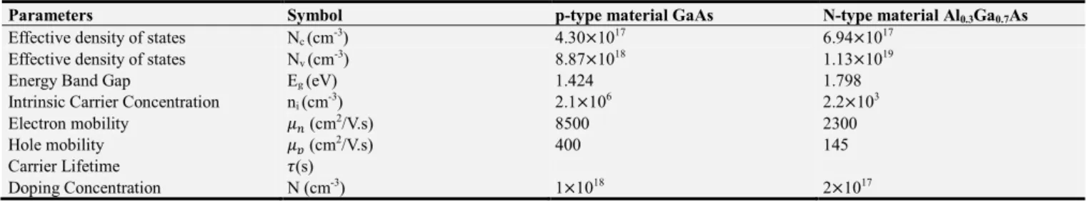
After calculating the required parameters, the efficiency needs to be obtained from this summarized parameters in Table 2.
Table 2. Parameters Used in Analysis of GaAs Heterojunction Efficiency.
Parameters Symbol p-type material GaAs N-type material Al0.3Ga0.7As
Effective density of states Nc (cm-3) 4.30 1017 6.94 1017
Effective density of states Nv (cm-3) 8.87 1018 1.13 1019
Energy Band Gap Eg (eV) 1.424 1.798
Intrinsic Carrier Concentration ni (cm-3) 2.1 106 2.2 103
Electron mobility U7 (cm2/V.s) 8500 2300
Hole mobility U (cm2/V.s) 400 145
Carrier Lifetime \(s)
Doping Concentration N (cm-3) 1 1018 2 1017
The diffusion lengths of the carriers can be described using carrier lifetime and diffusion lengths.
Lp = ]^ \ = 5.5 10-3cm
Ln = ]^7\7 = 1 10-3cm
For the light intensity, we will assume the standard intensity for solar cell, 85 mW/cm2. The cross-sectional area is supposed to be 0.15cm2. The absorption coefficients of p and N type are 2 103cm-1 and 4 104cm-1 respectively.
G = _`a*bYc = 7.08 1021cm-3/s
G = _`Yca*b = 1.42 1023cm-3/s
The built-in potential in a semiconductor equals the potential across the depletion region in thermal equilibrium.
Vbi = Y ln (
565<
7d ) = 1.586 V
The open-circuit voltage, Voc, is the maximum voltage available from a solar cell, and this occurs at zero current.
Voc = Y ln (
ef e$g 1
h =e$c = Y977ij56d + Y9 7i*5<d = 2.904 10-7 A/cm2
JL =
ek
c =qG ( Ln + Lp + xw) = 77.52 A/cm2
From the above two calculated results, the open-circuit voltage, Voc is 1.707 V.
The “fill factor”, more commonly known by its abbreviation ”FF”, is a parameter which, in conjunction with
Voc and Isc. The FF can be defined as the ratio of the maximum power from the actual solar cell to maximum power from the ideal solar cell. It can be calculated as:
FF = FF @%a; lm %a;I .%
a;I = 0.92
The efficiency is the most commonly used parameter to compare the performance of one solar cell to another. Efficiency is defined as the ratio of energy output from the solar cell to input energy from the sun.
η @ na;`djeop++ = 25.8 %
Plotting voltage-current characteristics of p-N junction.
3. AlGaInP Material
For AlGaInP heterojunction material, (AlxGa1-x)0.5In0.5P is
supposed to be used as ptype material and Al0.5In0.5P is used
as n-type material. For p-type material, its energy band gap can change from direct to indirect energy band gap according to the value of x which is the mole fraction, in other words, the composition of aluminium. For solar cells that perform high performance, the narrow energy band gap is needed and also indirect energy band gap is more prefer than direct energy band gap.
3.1. Energy Band Diagram of AlGaInP Heterojunction Material
To begin with energy band diagram, the respective energy band gap and its important parameters must be defined. For the mole fraction of (AlxGa1-x)0.5In0.5P , x = 0.5 wiil be
supposed because at that x value, the energy band gap is the narrowest and according to theoretical results, the energy band becomes indirect energy band gap when x > 0.48.
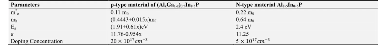
Table 3. Parameters For Calculating Energy Band Diagram of AlGaInP Heterojunction.
Parameters p-type material of (AlxGa1-x)0.5In0.5P N-type material Al0.5In0.5P
m*
e 0.11 m0 0.22 m0
mh (0.4443+0.015x)m0 0.64 m0
Eg (1.91+0.61x)eV 2.4 eV
11.76-0.954x 11.25
Doping Concentration 20 10 5 × 10
As the mole fraction of p-type material can be changed from x = 0 to 1, assume x= 0.5 and because of (AlxGa 1-x)0.5In0.5P heterojunction is applied to increase Voc, and lead
to higher fill factor (FF) and thereby higher power conversion efficiency. As the Al composition, x (AlxGa 1-x)0.5In0.5P exceeds 0.48, the band gap changes from direct to
indirect. By substituting x = 0.5, the parameters of p-type material can be obtained.
For the band edge discontinuities, the change of energy in conduction band, valance band and energy band gap can be obtained from Eq (3.3). Similarly, as calculated in previous section GaAs heterojunction, (AlxGa1-x)0.5In0.5P / Al0.5In0.5P
system.
For p-(AlxGa1-x)0.5In0.5P region,
* = 0.11 m0, * = 0.4518m0
Egp = 2.215eV, = 11.28
= 2( ∗ ) = 2.51× 10 ( . $×
$× ) =
9.16 × 10
% = 2( &
∗
) = 2.51× 10 ( .8# $×
$× )
= 7.62 × 10 p = '= Nv exp (
()* +*
) = 20 × 10
, − .% ≅ −012 ln(5)) = ≅ −012 ln(556)) = 34.59 meV
For N- Al0.5In0.5P region,
* = 0.22 m0, * = 0.64 m0
Egp = 2.4 eV, = 11.25
= 2( ∗ ) = 2.51× 10 ( . $×
$× ) =
2.59 × 10
% = 2( &
∗
) = 2.51× 10 ( ."8 $×
$× ) =
1.28 × 10
N = 9= Nc exp (
+: (;:
) = 5 × 10
.5− ,5≅ −012 ln(55)) = ≅ −012 ln(55<)) = 42.53 meV
The band edge discontinuities are
∆Eg = ∆EgN - ∆Egp = 0.185 eV
∆Ec = χ (n-type)- χ (p-type) = 4.2 - 3.709 = 491 meV,
∆Ev = ∆Ec + ∆Eg = 676 meV
Similar to GaAs heterojunction, the contact potential and depletion width of p-n junction need to be calculated in order to plot the energy band diagram. For these two parameters, the fundamentals and the related equations are described in Section 3, from Eq (3.13) to Eq (3.16).
V0 = Egp+∆Ec-(Fp-Evp)-(EcN -FN)/q (2215 + 491 - 34.59 -
42.53) mV V0 = 2628 mV
The depletion widths from p-side and N-side are
x?= [
BCD$
EFGFH(FHIJKJCFG)]
ND
= [ × . × . #8× MNO× .# "
."× MNP× × NR×#× NR×( × NRINN. Q
NN. [× × NR
] ×
5 × 10
= 1.81μm
xF=FsC
HNu = 7.24 μm
The total depletion width of p-n junction at equilibrium condition is
xv= x?+ xF = 9.05 μm
3.2. Efficiency
The efficiency of (AlxGa1-x)0.5In0.5P / Al0.5In0.5P
heterojunction material has to be computed in order to analyze how much percentage of the photon energy are absorbed by the solar cell as same with the calculation steps of GaAs heterojunction. The doping concentrations of the electrons and holes of the heterojunction material are designed as the same with the calculation of that of the energy band diagram.
For p-(AlxGa1-x)0.5In0.5P region,
μn = 475 cm2/V.s, μp = 7 cm2/V.s
Dn =
wx
E μn = 0.0259 × 475= 12.3 cm
2
/s
Dp =
wx
E μp = 0.0259 × 7 = 0.18 cm
2
Ny @ 9.16 10 cm , N| = 7.62 10 cm
For n- Al0.5In0.5P region,
μn = 100 cm2/V.s, μp = 10 cm2/V.s
Dn =
wx
E μn = 0.0259 100 = 2.6 cm 2
/s
Dp = Y Up = 0.0259 10 = 0.26 cm2/s
@2.59 10 , % = 1.28 10
The intrinsic carrier concentrations for both materials are
ni (For p-type) = Nc Nv exp (- (Z) = 3 106cm-3
ni (For N-type) = Nc Nv exp (- (Z) = 2 103cm-3
The diffusion lengths of the carriers can be described using carrier lifetime and diffusion lengths.
Lp = ]^ \ = 3.5 10-3cm
Ln = ]^7\7 = 1. 01 10-3cm
Table 4. Parameters For Analysis p-(Al0.5Ga0.5)0.5In0.5P / Al0.5In0.5P Heterojunction Efficiency.
Effective density of states Nv (cm-3) 7.62 1018 1.28 1019
Energy Band Gap Eg (eV) 2.215 2.4
Intrinsic Carrier Concentration ni (cm-3) 3 106 .2 103
Electron mobility U7(cm2/V.s) 475 100
Hole mobility U(cm2/V.s) 7 10
Doping Concentration N (cm-3) 20 1017 5 1017
For the light intensity, we will assume the standard intensity for solar cell, 85 mW/cm2. The cross-sectional area is supposed to be 0.15cm2. The absorption coefficients of p and N type are 1 106cm-1 and 4 105cm-1 respectively.
G = _`a*bYc = 3.54 1024cm-3/s
G = _`a*bYc = 1.42 1024 cm-3/s
The built-in potential in a semiconductor equals the potential across the depletion region in thermal equilibrium.
Vbi = Y ln (
565<
7d ) = 1.374 V
The open-circuit voltage, Voc, is the maximum voltage available from a solar cell, and this occurs at zero current.
Voc = Y ln (
ef e$g 1
h =ec$ = Y977ij56d + Y9 7i*5<d = 1.01 10-20 A/cm2
JL =
ek
c =qG ( Ln + Lp + xw) = 2468 A/cm2
From the above two calculated results, the open-circuit voltage, Voc is 1.39 V.
The “fill factor”, more commonly known by its abbreviation ”FF”, is a parameter which, in conjunction with Voc and Isc. The FF can be defined as the ratio of the
maximum power from the actual solar cell to maximum power from the ideal solar cell
FF @%a; lm %a;I .%a;I = 0.91
The efficiency is the most commonly used parameter to compare the performance of one solar cell to another. Efficiency is defined as the ratio of energy output from the solar cell to input energy from the sun.
η @ na;`eop++
dj = 14.88 %
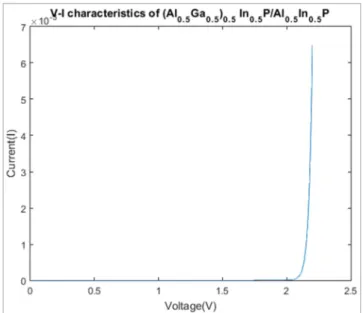
Plotting voltage-current characteristics of p-N junction,
Figure 3. Voltage-Current Characteristic of (Al0.5Ga0.5)0.5In0.5P / Al0.5In0.5P
Heterojunction Material.
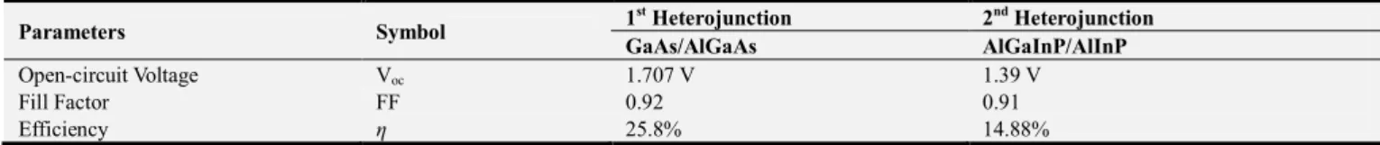
4. Comparison
Moreover, the fill factors of both materials are almost the same. In addition, the generation rate of AlGaInP heterojunction material is better than that of GaAs heterojunction material which means in the case of photon absorption, AlGaInP heterojunction can absorb well rather than GaAs heterojunction. However, for open-circuit voltage
of heterojunction materials, compared to each other, Voc of GaAs heterojunction is greater than Voc of AlGaInP heterojunction and therefore, the efficiency in which opencircuit voltage is partially included are totally different. The efficiency of GaAs is abou two times greater than that of AlGaInP heterojuction.
Table 5. Comparison between GaAs heterojunction and AlGaInP heterojunction.
Parameters Symbol 1
st Heterojunction 2nd Heterojunction GaAs/AlGaAs AlGaInP/AlInP
Open-circuit Voltage Voc 1.707 V 1.39 V
Fill Factor FF 0.92 0.91
Efficiency η 25.8% 14.88%
5. Discussions
First and foremost, the types of elements that are classified
as semiconductor materials and the most useful
semiconductors are presented in details. As the world energy consumption increases with time, the renewable energy resources are made to meet the shortage of natural energy resources. Solar cells are one of the solutions among the renewable energy resources. The research papers that are made experiments about the properties of semiconductor materials for solar cells have been presented with figures and calculation results. Secondly, the fundamental properties and some important parameters that will perform for all related equations have been described in details. The theories of p-n junction and the related equations to plot the band diagram of semiconductor material have been presented. This research work also includes the mathematical calculations that are required to obtain the characteristics of GaAs heterojunction and AlGaInP heterojunction by comparing with [3-6]. Finally, the voltage current characteristics and efficiencies for different mole fractions of semiconductor have been calculated and analyzed. Even though the lattice structures of GaAs and AlGaInP are matched to each other, their properties and their efficiency for solar cells are quite different from the above calculation results. The fill factors of both materials are almost the same and the generation rate of AlGaInP heterojunction material is better than that of GaAs heterojunction material. However, for open-circuit voltage of heterojunction materials, compared to each other, Voc of GaAs heterojunction is greater than Voc of AlGaInP heterojunction and therefore, the efficiency in which open-circuit voltage is partially included are totally different. The efficiency of GaAs is about two times greater than that of AlGaInP heterojuction. The computerized system is more effective than the manual analysis.
6. Conclusion
As a conclusion, materials having electrical conductivity value between that of conductors, like copper, gold, etc. and insulators such as glass can be defined as semiconductors and there are different kinds of semiconductor according to their belonging group in the periodic table. For the entire thesis, it can be said that there are various options in obtaining the
high performance solar cells and one of the option is choosing the narrow energy band gap for both p-type and n-type semiconductor materials. The purpose of applying the narrow energy band gaps rather than wide energy bands is that solar cells prefer narrow energy band gap to pursue the high efficiency and performance. The two semiconductor materials used in this research have narrow energy band gaps and The main process of this entire thesis is to analyze on band structure design of semiconductor materials for high performance solar cells using theoretical and mathematical approaches. First and foremost, the fundamental properties and some important parameters that will perform for all related equations have been described in details. The energy band gaps of p-n junction materials, the differences between fermi level energy and two energy band levels (conduction and valance) and dielectric constants have been calculated with mathematical equations. All of the parameters are derived at room temperature. The theories of p-n junction and the related equations to draw the band diagram of semiconductor material are presented. The depletion widths between p-n junction which depends on the contact potential and temperature are calculated and the temperature used in this case is assumed as room temperature. In addition, this thesis includes the steps of mathematical calculation that are required to obtain the characteristics of the individual semiconductor material. Secondly, the voltage current characteristics and efficiencies for different mole fractions of semiconductor is calculated and analyzed. Finally, other physical properties that are associated with the basic concepts of semiconductors have been included in this thesis. The electron and hole mobility and diffusion lengths for specific mole fraction of GaAs heterojunction and AlGaInP heterojunction have been obtained from using the existing parameters. Therefore, the fundamental needs for high performance solar cells and some essential properties are presented for this thesis development.
Acknowledgements
The author would like to thank many colleagues from the
Semiconductor Electronics Research Group of the
Department of Electronic Engineering of Yangon
References
[1] Mishra, U. and Singh, J. (2007). Semiconductor device physics and design. Springer Science & Business Media. [2] William J. Potscavage, J. Physics and Engineering of Organic
Solar Cells. PhD paper, Georgia Institute of Technology. [3] Cho, P. E. E. (2007). Analysis of V-I characteristics and
bandgap design for homojunction and heterojunction solar cells.
[4] Knechtli, R., Loo, R. Y., and Kamath, G. S. (1984). Highefficiency GaAs solar cells. IEEE Transactions on electron devices, 31(5): 577–588.
[5] Hwang, S.-T., Kim, S., Cheun, H., Lee, H., Lee, B., Hwang, T., Lee, S., Yoon, W., Lee, H.-M., and Park, B. Bandgap grading and Al 0.3 Ga 0.7 As heterojunction emitter for highly efficient GaAs-based solar cells. 155: 264–272.
[6] Cheong, J. S., Baharuddin, A. N. A. P., Ng, J. S., Krysa, A. B., and David, J. P. R. Absorption coefficients in AlGaInP lattice-matched to GaAs. 164: 28 – 31.
[7] Cheong, J. S., Ng, J. S., Krysa, A. B., Ong, J. S. L., and David, J. P. R. Determination of absorption coefficients in AlInP lattice matched to GaAs. 48(40): 405101.
[8] Neamen, D. A. Semiconductor Physics and Devices: Basic Principles. McGraw-Hill Education. Google-Books-ID: 2LwQPwAACAAJ.
[9] NSM archive - physical properties of semiconductors. [10] Neudeck, G. W. MODULAR SERIES ON SOLID STATE
DEVICES. page 229.
[11] C. C. Katsidis, A. O. Ajagunna, and A. Georgakilas, “Optical characterization of free electron concentration in heteroepitaxial InN layers using Fourier transform infrared spectroscopy and a 2×2 transfer-matrix algebra”, JOURNAL OF APPLIED PHYSICS 113, 073502, 2013.
[12] Yoshihiro Ishitani, “Theoretical and experimental study of the optical absorption at longitudinal phonon or phonon-plasmon coupling mode energy: An example of GaN”, Journal Of Applied Physics 112, 063531 (2012).