K.I. Udofia, D.N.Okoli IJSRE Volume 05 Issue 04 April 2017 Page 6357 Volume||5||Issue||04||April-2017||Pages-6357-6363||ISSN(e):2321-7545 Website: http://ijsae.in Index Copernicus Value- 56.65 DOI: http://dx.doi.org/10.18535/ijsre/v5i04.08
Investiagtion of The Optical, Structural And Surface Morphology Properties of Copper
Selenide Thin Films.
Authors
K.I. Udofia1, D.N.Okoli2
Department of Physics and Industrial Physics, Nnamdi Azikiwe University, Awka, Anambra State, Nigeria. Email:[email protected],
ABSTRACT:
Copper Selenide (CuSe) thin films were successfully electrodeposited onto a well cleaned glass substrate (ITO) at different deposition voltage, time and pH. The optical, structural and surface morphology properties of the films were studied by optical absorption analysis, x-ray diffraction and scanning electron microscopy (SEM) analysis respectively. The X-ray studied revealed that CuSe thin films show a hexagonal structure with lattice constant of a=5.852Å and possess polycrystalline nature. The grain size (D) increases as the deposition time increase, while the dislocation density decreases with increase in film thickness. The SEM micrographs revealed that the grains are small with varying size and evenly distributed throughout the smooth substrate surface. Optical absorption analysis revealed that CuSe thin films have band gap energy (Eg) values of 1.9eV-2.0eV. The high absorbance in UV region, high transmittance in VIS, NIR region and low reflectance, possesses by the films makes the materials applicable in P-N junction solar cells, solar energy collection and antireflective coating.
Keywords: Electro-deposition, Thin Film,CuSe, ITO, Optical, Characterization.
1. INTRODUCTION
Technological progress of modern society depends on the material science and engineering community’s ability to conceive the novel materials with extra-ordinary combination of physical and mechanical properties [1]. Most materials used in high technology applications are composites, i.e, they have a near-surface region with properties differing from those of the bulk materials. Most modern technologies require thin films for different applications. Thin film materials are key elements of continued technological advances made in the fields of optoelectronic, solar photovoltaic technologies, photonic, magnetic devices, microelectronic devices, magnetic thin films in recording devices, magnetic sensors, gas sensor, photoconductors, IR detectors, Super conductivity films, anticorrosive and decorative coating [2].
Thin film technologies make use of the fact that the properties such as optical, electrical, magnetic and structural properties are practically controlled by thickness parameter. These properties also depend on the methods of deposition, which are either physical or chemical methods.
K.I. Udofia, D.N.Okoli IJSRE Volume 05 Issue 04 April 2017 Page 6358 disadvantages. CuSe thin films have been prepared using various techniques, like chemical bath deposition [8], vacuum evaporation [9], and solution growth technique [10] etc has been prepared by many researchers. In this work, electrodeposition technique was used to grow copper selenide (CuSe) thin films onto an indium doped tin oxide (ITO) coated glass substrates, because of its unique advantages, such as low temperature growth, control of film thickness and morphology, high purity, rapidity, free from porosity, higher deposition rates, no post deposition treatment, large area deposition and cost effectiveness [11]. The investigation of the optical and structural properties of the thin films was done by subjecting the deposited CuSe thin films to optical absorption analysis, X-ray diffraction and scanning electron microscopy (SEM) analysis.
2. EXPERIMENTAL DETAILS
Copper Selenide (CuSe) thin Films were deposited by electro-deposition technique using the Copper II sulphate (CuSO4), Selenium dioxide (SeO2), Potassium Sulphate (K2SO4) and sulphuric acid (H2SO4).
Transparent medium doped tin oxide (ITO) coated glass was used as substrates. Aqueous electrolyte baths was prepared for the electrodeposition of Copper selenide (CuSe) thin Films. The baths was composed of 10cm3 of 0.09M of Selenium dioxide (SeO2), 10cm3 of 0.15m of Copper II sulphate (CuSO4), as source
selenium and copper ions respectively, mixed with 5cm3 of 0.14M of Pottasium Sulphate ((K2SO4), which
serve as the inert electrolyte that help to dissociate the selenium and copper to form the required CuSe thin film on the substrate. The solution was acidified with 3cm3 of 0.1M of Sulphuric acid (H2SO4), which adjust
the
pH-0.9. The entire mixture was stirred gently using a glass rod to achieve uniformity. The ITO Substrates were first washed with Acetone to remove any Impurity and then with methanol to remove residue as a result of the Acetone solvent, then finally rinsed with distilled water and dried before used. The conductivity side of the substrate were detected and dropped vertically into the electrolyte for the deposition process using hand gloves. The substrate (ITO glass) was connected to the negative terminal of the power source, while the carbon electrode was connected to the positive terminal for the deposition. Copper selenide thin film were deposited with variation of deposition voltage from (2.00V–10.00V), deposition time from (70.00s – 110.00s) and pH of the reaction bath from (1 – 1.2), while keeping the constant and temperature at 300K throughout the experiment. The substrates were removed at the end of the various voltage, time and pH intervals dried in clean air. M501 UV–VIS Spectrophotometer was used to obtain the absorbance values from the optical spectral analysis, the absorbance values and other optical and solid state properties were deducted. GBC eMMA x-ray mini-diffractometer using cukα (λ=1.5406Å) scanning from 17.26 to 25.15 degree was used for the X-ray diffraction characterization of the deposited CuSe thin Films, while the surface morphology of the films were carried out using scanning electron microscopy (SEM) machine. The Reaction Mechanism equation for the formation of the thin film are shown below
Cu2+ + 2e- Cu
The copper ion (Cu2+), is generated by the dissociation of CuSo4in water as
CuSo4 Cu2++ SO4
2-SeO2 +H2O H2SeO3
H2SeO3+ 4H+ + 4e- Se + 3H2O
Cu2++ Se + 2e- CuSe
3. RESULTS AND DISCUSSION
K.I. Udofia, D.N.Okoli IJSRE Volume 05 Issue 04 April 2017 Page 6359 voltage, time and pH values respectively. The figures revealed that the absorbance of the films increases with increase in wavelength deposition time and pH.
It shows generally that CuSe thin film has a high spectral absorbance in the UV region and moderate spectral absorbance in the IR region of the spectrum.
The high absorbance in UV region makes CuSe thin films material applicable in the formation of p-n junction solar cells and other suitable materials for photovoltaic application. Figures 3.4, 3.5 and 3.6 shows the optical transmittance spectra of CuSe thin films.
Figure 3.4 shows that the transmittance spectra of the films increase with the wavelength from UV region through Vis region to NIR region, with highest value of 0.94% in NIR region for film deposited at 60s, 8V. Figure 3.5 revealed highest value of transmittance of 0.82% in NIR region for film deposited at 2V, 110s with an evident that transmission increases with deposition time.
Generally the figures revealed that the deposited CuSe thin films has high transmittance in the VIS and NIR region of the spectrum, which makes the materials desirable for solar energy collection and a good material in the production of blue and green light emitting device.
Fig.3.1: Plot of absorbance against wavelength for CuSe thin films at different voltages
K.I. Udofia, D.N.Okoli IJSRE Volume 05 Issue 04 April 2017 Page 6360 Fig.3.3: Plot of absorbance against wavelength for CuSe thin films at different pH
Fig.3.4: Plot of transmittance against wavelength for CuSe thin films at different voltages
Fig.3.5: Plot of transmittance against wavelength for CuSe thin films at different time intervals
K.I. Udofia, D.N.Okoli IJSRE Volume 05 Issue 04 April 2017 Page 6361 Figures 3.7, 3.8 and 3.9 show the reflectance spectra of the deposited CuSe thin films at different deposition voltage, time and pH.
The figures revealed that the films reflect in UV region, VIS and IR region of electromagnetic spectrum, with the highest reflectance value in the UV region.
Generally, the reflectance is low and this low reflectance makes the material useful in antireflective coasting and also close to properties desired for solar control coating. It was clear from the figures 3.10, 3.11 and 3.12 that there refractive index of CuSe thin films increases with increase in photon energy, with values ranging from 1.4 – 2.4 within photon energy of 1.4 – 4.2eV for the variation of deposition voltage, time and pH. This value of refraction index makes the material suitable for use in optoelectronic devices.
Fig.3.7: Plot of reflectance against wavelength for CuSe thin films at different voltages
Fig.3.8: Plot of reflectance against wavelength for CuSe thin films at different time intervals
K.I. Udofia, D.N.Okoli IJSRE Volume 05 Issue 04 April 2017 Page 6362 Fig.3.10: Plot of refractive Index against photon energy For CuSe thin films
Fig.3.11: Plot of refractive index against photon energy for CuSe thin films.
K.I. Udofia, D.N.Okoli IJSRE Volume 05 Issue 04 April 2017 Page 6363 The band gap and nature of transition of the deposited CuSe thin films was determined by using the
following relation [12].
α = (hf – Eg)n/2
[1 ]
When hf is the photon energy and Eg is the band gap, with n having the value of 1 or 4 for direct transition and indirect transition respectively.
Extrapolating the straight part of the graph of absorption coefficient square against the photon energy axis, give the band gap energy,(Eg) of the deposited CuSe thin film. Figure 3.13, 3.14 and 3.15 revealed that the band gap values ranges from 1.9ev – 2ev and the straight nature of the plot revealed a direct transition
Fig.3.13: Plot of absorption coefficient square against photon energy for CuSe thin film (CuSeA)
K.I. Udofia, D.N.Okoli IJSRE Volume 05 Issue 04 April 2017 Page 6364 Fig.3.15: Plot of absorption coefficient square against photon energy for CuSe thin film (CuSe K)
3.2 Structural Properties of CuSe thin Films.
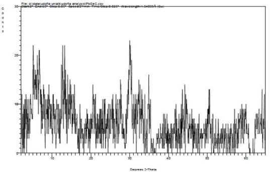
The X-ray Diffractograms of CuSe J, and CuSe A, thin films obtained at deposition time and voltage of 110s, 2v and 70s, 2v respectively are shown in figures 3.16 and 3.17
Figure 3.16 for CuSe J revealed that the diffraction peaks occurs at 21.53°, 22.44°, 23.23°, and 24.24° with the spacing 3.122A, 3.132A, 3.139A and 3.146A corresponding to lattice plane (111), (220), (311) and (4000) respectively.
Figure 3.17 shows that the diffraction peaks and found at 20.12°, 22.32°, 24.99°, and 25.38° with the spacing of 3.101A, 3.122A, 3.137A and 3.144A respectively, the corresponding lattice plane are (111), (220), (311) and (400)
The XRD pattern for the CuSe thin film generally show a polycrystalline in nature with hexagonal structure and lattice constant a=5.852. This result is in close agreement with the result reported by Bari et al; [2008]. Ramesh et al,. [2013].
Table 4.1 and 4.2 shows the grain size (D), Dislocation density (δ) of the film determined by using Scherer equation [13].
D= 0.9λ cos
Where λ is the wavelength of Cukα (λ=1.5406Å), is the full width at half maximum of the peaks position in radians and is the bragg diffraction angle.
The dislocation density (δ) and micro strain (ɛ) were calculated using the following equation.[14,15] Dislocation density:
δ= 1 [3] 4tan
Micro strain:
K.I. Udofia, D.N.Okoli IJSRE Volume 05 Issue 04 April 2017 Page 6365 Table 3.1 and 3.2 revealed that the grain size (D) for the deposited films increases with increase in film thickness, with an average grain size(D) of 7.27nm and 13.138nm for CuSe J, and CuSe A of thickness 135nm and 172nm respectively.
It also revealed that the grain size also increases as the deposition time increase. While the dislocation density decreases with increase in film thickness, micro strain increases with film thickness.
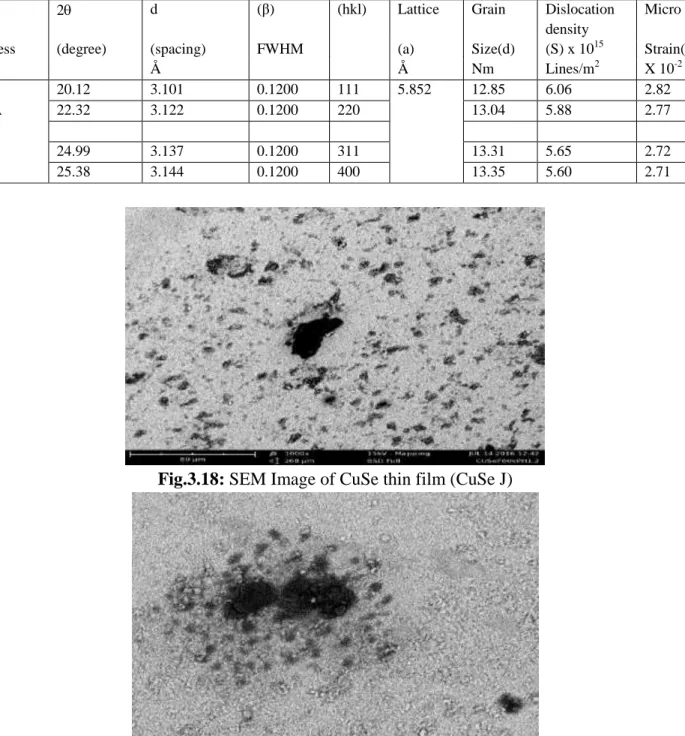
Figure 3.18 and 3.19 show the SEM micrographs of 4000X magnification for copper selenide thin film sample, CuSe J, and CuSe A.
The Micrographs revealed that the grains are small with varying sizes and evenly distributed throughout the smooth substrate surface, and are almost spherical in shape. This suggests that the materials are polycrystalline in nature, which is in good agreement with the XRD results.
Fig.3.16: X-ray Diffraction Pattern of CuSe thin film (CuSe J)
K.I. Udofia, D.N.Okoli IJSRE Volume 05 Issue 04 April 2017 Page 6366 Fig.3.18: SEM Image of CuSe thin film (CuSe J)
Fig. 3.19: SEM Image ofCuSethin film (CuSe A)
Sample 2 d (β) (hkl) Lattice Grain Dislocatio
n density
Micro Strain(Ɛ)
Thickness (degree) (spacing) FWHM (a) Size(D) () x 1016
Å Å Nm Lines/m2 X 10-2
21.53 3.122 0.2160 111 5.852 7.206 1.93 5.02
CuSe J 22.44 3.132 0.2160 220 7.253 1.90 4.99
135nm
23.23 3.139 0.2160 311 7.296 1.88 4.96
24.24 3.146 0.2160 400 7.350 1.85 4.92
Sample 2 d (β) (hkl) Lattice Grain Dislocation
density
Micro
Thickness (degree) (spacing) FWHM (a) Size(d) (S) x 1015 Strain(Ɛ)
Å Å Nm Lines/m2 X 10-2
20.12 3.101 0.1200 111 5.852 12.85 6.06 2.82
CuSe A 22.32 3.122 0.1200 220 13.04 5.88 2.77
172nm
24.99 3.137 0.1200 311 13.31 5.65 2.72
25.38 3.144 0.1200 400 13.35 5.60 2.71
Table 3.1: Structural parameters of CuSe thin film (CuSe J)
K.I. Udofia, D.N.Okoli IJSRE Volume 05 Issue 04 April 2017 Page 6367 CONCLUSION
Electro-deposition technique was used to deposit CuSe thin Films on ITO substrate at different deposition voltage, time and PH. The optical absorption analysis revealed that CuSe thin films have high spectral absorbance in the UV region and moderate absorbance in the IR region. The transmittance was high in the VIS and NIR region of the Spectrum. The films also show a low reflectance in the UV and Vis regions. A direct transition band gap value of ranges from 1.9ev – 2ev was determined for the thin film. These optical properties make the materials desirable for p-n junction, solar cell, solar energy collection and antireflective coasting.
REFERENCES
1. Glocker, and I. Shah (2002): “Handbook of thin film process Technologies Institute of Physics vol. 1 and 2
2. Bunshad, Rodtan F (1994): “Handbook of deposition Technologies for films and coatings” Second Edition”
3. Chen H, Shi D, Wang J. B. (2009):“The stability and electronic properties of Wurtzife and Fine – blende FnS namowire physics” physics letters, A Vol. 373. PP 371 – 375.
4. Hankare P. P, Khomane .A. S, Chate .P. A, Rathid .K. C, Garadkar K. M. (2008):“Preparation of Copper sclenide thin films by simple chemical route preempt at low temperature and their characterization.
5. Okereke N. A., Ekpunobi A. J. (2010): “Structural and optical studies of chemical bath deposited lead selenide (PbSe) thin films.
6. Sadekar H. K.(2011) “Optical and structural properties of PbSe thin film deposited by chemical bath deposition”.
7. Ramesh K. Bharathi B, Thanidkaidarasam S, Mahalongam T, Sebastian P.J (2013):“Growth and characterization of electroplated Copper Selenide thin films.
8. Bari R. H, Ganesan V, Potadar S. and Patil L.A. (2009):. Mater Sci., 32,37.
9. Chen. W. S., Stewart J.M. and Mickelso, R.A.(1985): Appl, phys. Let.,46, 1095-2000
10.Gosavi S.R, Deshpande N.G, Gudage Y.G., Ramphal Sharma.(2000): “Physical, optical and electrical properties of copper selenide (CuSe) thin films deposited by solution growth technique at room temperature”.
11.Sethuramechandram, Thanikaikarasan thaiyan mahalingam. V. Phanasekaran (2012):“Growth and characterization of lead selenide thin films.
12.Ashour A.(2003): Turk. J. Phys. 27,551.
13.Cullity B.D (1967): “Elements of X-ray diffraction,’’ 3rd printing.
14.Thanikadkarasan S., .mahalingam T. (2012): Alloy. And Compd. 511, 155