DC Treasure Box
ELECTRICAL ENGINEERING DEPARTMENT
California Polytechnic State University
Senior Project 2020
Advisor DavidBraun
Author
Contents
List of Figures iv
List of Tables v
1 Intro 2
2 Customer Needs Assessment 3
3 Planning 9
4 Progress 17
4.1 Project Timeline . . . 17
4.2 Project Cost . . . 20
5 Design 23 5.1 Power Supply Design . . . 24
5.1.1 Component Selection . . . 28
5.2 Source Measure Unit Design . . . 29
5.2.1 Revision A . . . 30
5.2.2 Revision B . . . 33
5.2.2.1 Voltage Limiting . . . 34
5.2.2.2 Current Limiting . . . 36
5.2.3 Revision C . . . 38
5.3 Analog Input Output . . . 41
5.3.1 Analog Input . . . 41
5.3.2 Analog Output . . . 43
5.4 Digital Input Output . . . 45
5.4.1 Digital Input . . . 45
5.4.2 Digital Output . . . 46
6 Testing 47 6.1 Power Supply . . . 47
6.1.1 Line Regulation . . . 48
6.1.2 Load Regulation . . . 50
6.1.3 Current Limiting . . . 51
6.1.4 Transients . . . 55
6.2 SMU . . . 57
6.2.1 Early Prototype . . . 57
6.2.2 Voltage Mode . . . 59
6.2.3 Current Mode . . . 62
6.3 AIO . . . 63
6.3.1 Analog Output . . . 63
6.3.2 Analog Input . . . 66
6.4 DIO . . . 68
6.4.1 Digital Output . . . 68
7 Conclusion 72
8 Errata 74
8.1 Power Supply . . . 74
8.2 SMU . . . 76
8.3 AIO . . . 79
8.4 DIO . . . 81
8.5 µC Board . . . 82
9 Appendices 83 9.1 Schematics . . . 83
9.1.1 Power Supply Revision A . . . 84
9.1.2 Power Supply Revision B . . . 85
9.1.3 SMU Revision C . . . 86
9.1.4 SMU Revision D . . . 91
9.1.5 Analog/Digital Input/Output Revision A . . . 96
9.1.6 Analog/Digital Input/Output Revision B . . . 101
9.1.7 µC Revision A . . . 106
9.1.8 µC Revision B . . . 109
9.2 Layouts . . . 112
9.2.1 Power Supply Revision A . . . 112
9.2.2 SMU Revision C . . . 113
9.2.3 Analog/Digital Input/Output Revision A . . . 114
9.2.4 µC Revision A . . . 115
9.3 Fabricated Boards . . . 116
9.3.1 Power Supply Board . . . 116
9.3.2 SMU Board . . . 117
9.3.3 Analog/Digital Input/Output Board . . . 118
9.3.4 µC Board . . . 119
9.4 Survey . . . 120
9.5 Survey Optimization and Analysis . . . 125
9.6 Code . . . 130
9.7 Demo Video . . . 130
9.8 Experiments . . . 131
9.8.1 BJT Thermometer Viability . . . 131
9.8.2 Output Voltage Limitations Sweep . . . 134
9.8.3 Diff-Pair Voltage Sweep . . . 136
9.8.4 Common Emitter Sweep . . . 138
9.8.5 Current Mirror Sweep . . . 140
9.9 ABET Analysis . . . 142
9.9.1 Summary of Functional Requirements . . . 142
9.9.2 Primary Constraints . . . 142
9.9.3 Economic . . . 142
9.9.4 If manufactured on a commercial basis . . . 143
9.9.5 Environmental . . . 145
9.9.6 Manufacturability . . . 145
9.9.7 Sustainability . . . 145
9.9.9 Health and Safety . . . 146
9.9.10 Social and Political . . . 146
9.9.11 Development . . . 147
9.10 Special Thanks . . . 150
9.10.1 Component Graveyard . . . 150
List of Figures
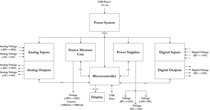
3.1 Full System Black Box Diagram . . . 10
3.2 Full System Subsystem Diagram . . . 11
3.3 DC Power Supplies Black Box Diagram . . . 12
3.4 Source Measure Unit Black Box Diagram . . . 13
3.5 Analog Input/Output Black Box Diagram . . . 14
3.6 Digital Input/Output Black Box Diagram . . . 15
3.7 Microcontroller Black Box Diagram . . . 16
4.1 Fall Quarter Gantt Chart . . . 17
4.2 Winter Quarter Gantt Chart . . . 18
4.3 Spring Quarter Gantt Chart . . . 19
4.4 Total Project Costs, Including Board Fab and Shipping . . . 20
5.1 Functional Block Diagram of the LM317 in Adjustable Voltage Regulator Configuration . . 24
5.2 Simplified Block Diagram of the LM317 . . . 25
5.3 Positive Power Supply Design with Characterized Load . . . 26
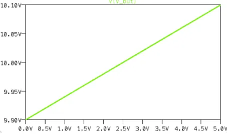
5.4 Output Voltage VS DAC Voltage . . . 26
5.5 Output Transients for Selected Load Characterizations . . . 27
5.6 Result of an ESR of 1Ω . . . 27
5.7 Result of Testing a Diode with a Current Limit of 0.1A . . . 29
5.8 Bidirectional Current Source/Sink using the INA105 [6] . . . 30
5.9 Current Source/Sink Implemented (Red Highlight Shows Active Circuitry) . . . 30
5.10 Precision ±10V Voltage Source using the INA105 [7] . . . 31
5.11 Precision ±10V Voltage Source Implemented (Green Highlights Active Circuitry) . . . 31
5.12 Reduction in Output Impedance of the SMU . . . 32
5.13 SMU Voltage Limiting Circuit . . . 34
5.14 SMU Voltage Limiting Transient Simulation (Sourcing Current) . . . 35
5.15 SMU Voltage Limiting Transient Simulation (Sinking Current) . . . 35
5.16 SMU Current Limiting Circuit . . . 36
5.17 SMU Voltage Limiting Circuit (Positive Voltage Output) . . . 37
5.18 SMU Voltage Limiting Circuit (Negative Voltage Output) . . . 37
5.19 Fine and Coarse Control Hardware Realization . . . 39
5.20 Fine and Coarse Control Hardware Realization With One Less Op-Amp . . . 39
5.21 Output of Fine/Coarse Control for Voltage Mode . . . 40
5.22 Output of Fine/Coarse Control for Current Mode . . . 40
5.23 Input Circuity to the Analog to Digital Converter . . . 41
5.24 Output Circuity for the Digital to Analog Converter . . . 43
5.25 INA145 Adjustable Gain Difference Amplifier Design Recommendations 20 . . . 44
5.26 Graph Showing Threshold Voltage Set From Average of TTL Voltage Levels . . . 45
5.27 Digital Input Structure with ESD/Overvoltage Protection . . . 45
5.28 Digital Output Structure . . . 46
6.1 Power Supply Output vs Input Voltage . . . 48
6.2 Voltage % Error at Selected Set Voltages . . . 48
6.3 Measured % Error plotted on same axis of Error Specifications . . . 49
6.4 Variation in Output Voltage for Different Loads . . . 50
6.5 Current Demand of Different Loads . . . 50
6.8 Alert Voltage Triggering on Overcurrent Event . . . 52
6.9 100Ω Load with a 0–10V Step and 50mA Current Limit Load Voltage (Orange) and Alert (Green) . . . 53
6.10 Step Response of Positive Power Supply Under Various Loading conditions . . . 55
6.11 Power Supply Terminals Directly Shorted Transient . . . 56
6.12 SMU Early Prototype on Breadboard . . . 57
6.13 Voltage and Current Transfer Characteristics of Proto-SMU . . . 58
6.14 SMU Voltage Transfer Characteristic . . . 59
6.15 Measured Output Error with Original and Updated Specifications . . . 59
6.16 Load Regulations for Selected Output Voltages . . . 60
6.17 % Error of Load Voltages . . . 60
6.18 Resistors in Output Signal Path . . . 61
6.19 SMU Current Transfer Characteristic . . . 62
6.20 Measured Output Error with Original and Updated Specifications . . . 62
6.21 % Error of Current Mode (Zoomed Out View) . . . 63
6.22 % Error Before and After Calibration (Output Channel 3) . . . 64
6.23 % Error Before and After Calibration (Output Channel 0) . . . 64
6.24 % Error with Zero, One, and Two Calibration Passes (Input Channel 3) . . . 66
6.25 % Error One and Two Calibration Passes (Input Channel 3) . . . 66
6.26 % Error After Two Calibrations with Error Bounds (Input Channel 3) . . . 67
6.27 Output Voltage Transfer Characteristics of Digital Outputs . . . 68
6.28 % Error of Digital Outputs . . . 68
6.29 Fall time of Digital Output with a load of 2kΩ || 1000pF . . . 69
6.30 Input (Orange) and Output (Green) of Digital Input withVtrip set to 2.5V . . . 70
6.31 Input (Orange) and Output (Green) of Digital Input Filter . . . 70
6.32 Clamped Input . . . 71
7.1 How is this even possible . . . 72
7.2 Lest anyone want to attempt to tame the Hell Circuit . . . 73
8.1 Schematic of Power Supply Showing Error and Correction . . . 74
8.2 Roman Numeral Realization in Hardware . . . 75
8.3 Corrected Pinout with Bent Leads . . . 75
8.4 Modified Fine/Coarse Control and Voltage Conditioning Circuits . . . 76
8.5 A Fun Game of Spot the Difference . . . 77
8.6 Switcharoo Attended To . . . 77
8.7 Gain as a Function of 2 Resistor Tolerance Ranges . . . 79
8.8 The Results of Two Hours of Soldering . . . 82
9.1 Test Setup for Generating I-V Curve . . . 131
9.2 I-V Curve (Zoomed Out) . . . 131
9.3 I-V Curve (Zoomed In) . . . 132
9.4 Test Setup for Measuring Output Voltage Swing . . . 134
9.5 Op Amp Sweeps . . . 135
9.6 Test Setup for Measuring Differential Pair Transfer Characteristics . . . 136
9.7 ECL Voltage Transfer Characteristic . . . 137
9.8 Test Setup for Measuring Common Emitter Characteristics with Different Base Currents . . 138
9.9 Test Setup for Measuring Common Emitter Characteristics with Different Base Currents . . 139
9.10 Using Effective-Base-Width Modulation to Extrapolate Early Voltage . . . 139
9.11 Test Setup for Measuring Current Mirror Characteristics . . . 140
List of Tables
2.1 Selected Survey Responses . . . 4
2.2 Power Supply Specifications . . . 5
2.3 Source Measure Unit Specifications . . . 6
2.4 Analog Input Output Specifications . . . 7
2.5 Digital Input Output Specifications . . . 8
3.1 Total System Description . . . 10
3.2 DC Power Supplies Description . . . 12
3.3 Source Measure Unit Description . . . 13
3.4 Analog Input/Output Description . . . 14
3.5 Digital Input/Output Description . . . 15
3.6 Microcontroller Description . . . 16
4.1 Power Supply BOM . . . 21
4.2 SMU BOM . . . 21
4.3 AIO/DIO BOM . . . 22
4.4 Misc. BOM . . . 22
6.1 Output Voltage of Each Supply From a Given Hexadecimal Code . . . 47
8.1 Resistor Changes Made to SMU Rev C . . . 76
9.1 R.I.P. . . 150
9.2 Beloved Wife and Mother . . . 151
9.3 F . . . 151
9.4 Gone but not Forgotten . . . 152
9.5 RIP in Peace . . . 152
9.6 Wounded in Battle, in Stable Condition . . . 153
Abstract
1 Intro
Either write something worth reading or do something worth writing.
Benjamin Franklin
2 Customer Needs Assessment
It is always great when people take interest in your work.
Margaret H. Hamilton
When building circuits, either as a electronics hobbyist, student, or professional, it is important to own an adjustable power supply that provides the proper voltages and currents needed. Additionally, multimeters are crucial to take various measurements to verify that a circuit is biased correctly and operating as expected. This equipment, alongside oscilloscopes and function generators, can be expensive and bulky
1-2. This senior project aims to satisfy the need for an adjustable power supply and multimeter whilst staying relatively cheap and compact.
To ensure that this product is desirable to the target markets, a survey given to 30 upper division EE/CPE students attending Cal Poly San Luis Obispo drove the requirements and functionality of the project 30. Questions included indicating desired power supply voltage and current range, multimeter resolution, additional functionalities, and price.
The survey showed a high importance placed on ohmmeter functionality and power supplies with adjustable current limits, with at least 85% of surveyed students stating both having an ohmmeter is important and they use current limits with lab equipment.
Additional customer needs are drawn from the electronics lab series given during the course of un-dergraduate studies at Cal Poly. The capabilities of the project allow it to characterize components and achieve proper DC-biasing for any circuit given during the electronics lab series. Miscellaneous features such as a continuity checker provide quality of life.
Other customer needs come from analyzing the capabilities of existing benchtop and portable DC resources such as the Agilent E3631A power supply, Keithley 2400 Sourcemeter, and the Analog Discovery 2. The DC Treasure Box is expected to provide performance mimicking some of the capabilities and features of these devices. The product directly competes with Analog Discovery 2, commercial multimeters, and commercial power supplies. It is seen as an alternative to these products, abet somewhat more limited in some aspects.
Market research done for this project came from a survey given out to Cal Poly students. Section9.4in the Appendices shows the survey and complete dataset. Table 2.1 shows selected results at a glance. As part of a project for IME 305 (Operations Research II), the author used a linear programming optimization model to determine the best specifications to focus on given limited time and budget. However, this model was made during Spring Quarter and had no role in determining the specifications. Section 9.5 shows the results of the model.
Table 2.1. Selected Survey Responses
Specification: Highest Response % of Response
Power Supply Voltage Range -12 – 12V 56.7%
Power Supply Current Range >1 A 50%
Multimeter Resolution 50µV 43.3%
Current Limiting Yes 83.3%
3 Planning
Above all, don’t fear difficult moments. The best comes from them.
Rita Levi-Montalcini
Due to the project’s somewhat ambitious nature careful thought is put into the total system design. These considerations include power, communication, and design flexibility.
Tradeoffs are made, ensuring the project is feasible for a single undergraduate student to make over the course of less than a year with a budget of a few hundred dollars. Typical power supplies can deliver large amounts of power. The power supplies for this project are far weaker than those on the market. Each power supply can only deliver about 2 watts of power. As the project’s purpose is providing a cheap, portable lab environment capable of completing undergraduate laboratory experiments.
Market SMUs and multimeters can of measure (or in the SMU’s case, output) kV level signals. The SMU built in this project can only measure/supply voltages from 10V — 10V, and currents of 500µA -100mA. The upside is that the SMU in this project is built for less than $100, and by a single person.
Figure 3.1. Full System Black Box Diagram
Table 3.2. DC Power Supplies Description
Table 3.3. Source Measure Unit Description
Table 3.4. Analog Input/Output Description
Table 3.5. Digital Input/Output Description
Table 3.6. Microcontroller Description
4 Progress
4.1 Project Timeline
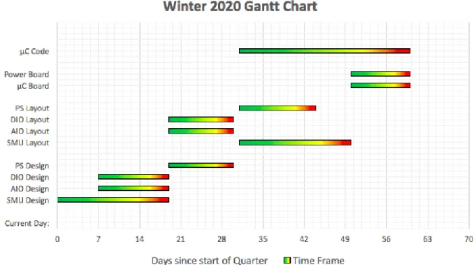
Each Gantt Chart corresponds a different quarter during the academic years of 2019 to 2020.
Figure4.1shows the Fall 2019 Quarter Gantt chart. The chart starts on September 1st, 2019, and counts the days passed since then. Each major event is given an estimated start and end date, which the graph plots. The Specifications and Literature Search are given the most time to complete. The specifications are crucial to get correct, if they are impossible to achieve or not desirable to potential customers the project would be set back significantly. The Literature Search spans the entire quarter as it pertains to every aspect of the project. Sources include design documents, market research, competition analysis, and application notes.
Figure 4.2 shows the Winter 2020 Quarter Gantt chart. This chart is primarily focused on subsystem design and layout. The SMU design is by far the most complicated, so it is allocated the most time. The AIO/DIO layout was simplified as they share the same board. This reduces the amount of µC/power supply connections. The µC code involved setting up communcations with the various DACs/ADCs. The project uses 6 different DACs/ADCs chips, meaning this was a lengthy process. The Power Board task is not completed during the Winter Quarter, and is pushed back to Spring Quarter. However, due to time constraints, the author ops to buy a pre-made switch-mode power supply board.
Figure 4.2shows the Spring 2020 Quarter Gantt chart. The quarter is focused on testing, integration, and final report writing. Design and Testing report sections are written as each subsystem completes verification. The µC board acts as a motherboard for the MSP432P401R Launchpad. The Launchpad slots in and has relevant pins mapped to various connectors. The Automation task is the final endeavor; it entails the synchronization of all the subsystems to provide with an automated test/measurement suite.
4.2 Project Cost
To provide an affordable price to students, the target project price is roughly $200. Figure4.4shows the cost breakdown by subsystem. All component costs are calculated assuming a 100 unit purchase quantity. The SMU subsystem was the most expensive. It costs about as much as the power supply and AIO/DIO combined. The bulk of the SMU cost came from the OPA633 ($15.06), INA105 ($9.38), and 4 relays ($2.33 each). These three part types account for more than a third of the total board cost.
Table 4.1. Power Supply BOM
Table 4.3. AIO/DIO BOM
5 Design
If analog people can do stupid things, can stupid people do analog things?
Bob Pease
5.1 Power Supply Design
Informally, the power supply requirements are straightforward. The crux of the design is finding a suitable configuration that can vary the voltage at the lower range. A brief look at various linear regulators suggests that this a ‘weak point’ in their use, as a typical LDO output has a lower limit of roughly 1 – 2V. A look under the hood shows us why this is the case.
Figure 5.1. Functional Block Diagram of the LM317 in Adjustable Voltage Regulator Configuration [16]
Figure 5.2. Simplified Block Diagram of the LM317
Figure 5.2 shows the simplified LM317 voltage control system. The op-amp U1 is a voltage follower; the voltage at the inverting and non-inverting terminals is approximately the same. This forces a constant 1.25V across R1. As the op-amp terminals ideally draw no current, all the current through R1 passes
through R2. Equation 1 shows the output voltage as a function of the reference voltage Vz and resistor ratio.
Vout =Vz∗(1 +
R2
R1) (1)
Most notably shown above is that the output voltage can only reach a minimum ofVz. For the LM317,
Vzis 1.25V, and is a reference voltage that manifested either through a Zener diode or a bandgap reference. This voltage is designed to be sturdy under temperature and not vary under normal operating conditions. Another takeaway is the ratio of R2 toR1 sets the ratio of output voltage to reference voltage. IfR1/R2
is adjustable, the output voltage varies in a predictable fashion.
Figure 5.3. Positive Power Supply Design with Characterized Load
The voltage VDAC is referenced to ground, meaning that whatever the DAC voltage appears across R2
instead ofR1. Equation2 shows the output voltage as a function ofVDAC.
Vout =Vz∗(1 +
R2
R1
) (2)
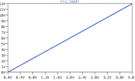
As typical DACs typically output 0 – 5V, and the power supply output is 0 – 12V, a 2:1 resistor ratio sets the overall gain to 3V/V. A DAC voltage of 4V results in an output voltage of 12V. Figure5.4shows the DC transfer characteristic.
One concern of the design shown in figure 5.3 is stability for large capacitive loads. As this module is used as a power supply, the user may attach large value bypass capacitors to the output. The overall system stability is tested using a DAC output 4V step at t = 1ms for a variety of load conditions.
(a) Load = 100Ω || (10nF + 0Ω) (b) Load = 100Ω || (1µF + 0Ω)
(c) Load = 100Ω || (2µF + 0Ω) (d) Load = 100Ω || (2µF + 1Ω)
Figure 5.5. Output Transients for Selected Load Characterizations
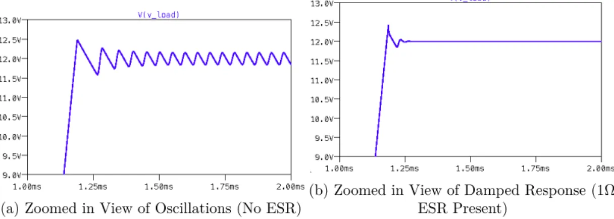
Figure 5.5show the effect of different load capacitors on the power supply stability. Figures 5.5a and
5.5b show how small capacitance values and no capacitor equivalent series resistance (ESR) results in a stable output. However, once the load capacitance passes a certain point, the output begins to oscillate. Figure 5.5c shows the output oscillation for a load of 100Ω in parallel with a 2µF capacitor with 0 ESR. Figure 5.6a shows the zoomed in oscillation. These oscillations vanish when the capacitor has roughly a few ohms of ESR. Figures5.5d and 5.6bshow the now damped response.
(a) Zoomed in View of Oscillations (No ESR)
(b) Zoomed in View of Damped Response (1Ω ESR Present)
Potential instability is a common problem when working with linear regulators15. Based on figure 5.6, the power supply topology presented is stable.
5.1.1 Component Selection
The DAC chosen is the BU2507FV. This particular DAC has 6 outputs, fulfilling the demand of the 3 voltage control channels and 3 current limit channels. The BU2507FV is 10-bit, which allows a 14.65mV resolution in the power supply output.
The REF5050 is a 0.01% 5V reference capable of sourcing 10mA of current [21]. Because the output current is greater than the BU2507FV maximum current demand, the REF5050 can power the DAC. This saves the board from needing a separate 5V power and 5V reference voltage.
The series pass transistors used are chosen based on of power dissipation, maximum DC collector current, and maximum collector-emitter voltage. BJTs in TO-220-3 packages are desirable for the ability for the addition of a heat sink. The TIP32BG and BD239C are chosen. Both devices have power dissipation (at
5.2 Source Measure Unit Design
The Source Measure Unit (SMU, or also affectionately known to me as the Hell Circuit) proved to be the most difficult module to design. The base functionally of force current, measure voltage and force voltage, measure current was achievable with some research and luck. At low voltages and currents there is no need for range switching, removing a potentially complicated block of a normal SMU. The currents and voltages measured are also in a goldilocks zone; not too small that special considerations are needed for acceptable measurement accuracy and not too large that power dissipation and voltage/current ratings need to be closely examined. The difficult part of designing the SMU was the current and voltage limiting sub-circuits. The project’s author for reasons unbeknownst to anyone, decided that in the event of an overvoltage/overcurrent situation, the SMU goes into either constant current or constant voltage mode, rather than turn off. Figure5.7shows an example of this behavior.
Figure 5.7. Result of Testing a Diode with a Current Limit of 0.1A
5.2.1 Revision A
The first attempt at the SMU resulted in a viable circuit in terms of voltage/current output specs. Voltage/current limiting features were not present, and had a 50Ω output impedance in voltage source mode which needed correction. Despite these problems, REV A formed the foundation for subsequent revisions. The SMU REV A design is primarily based on two separate application notes. The first is a 1990 Burr Brown paper concerning implementation and uses of current sources and receivers. The second is a 2000 TI application note on a precision ±10V voltage source. By a stroke of luck, both app notes reference the INA105, a precision unity gain amplifier. Relevant images from both app notes and the corresponding implementation are shown in figures5.8and 5.10.
Figure 5.8. Bidirectional Current Source/Sink using the INA105 [6]
Figure 5.9. Current Source/Sink Implemented (Red Highlight Shows Active Circuitry)
According to the application note, the differential voltage as well as the resistor R set the current delivered to the load [6]. When R is 50Ω, a ±5V differential voltage results in a ±100mA current. In figure
5.9, the input toU1, is 0-10V. When using a 5V reference voltage, a ±5V differential voltage occurs. With
Figure 5.10. Precision ±10V Voltage Source using the INA105 [7]
Figure 5.11. Precision ±10V Voltage Source Implemented (Green Highlights Active Circuitry)
In figure 5.11, the input voltage into U1 varies between 0 – 10V. The non-inverting input to INA105 U1 is a 10V reference, as per the app note. With this configuration the output voltage of U1 is -10 to 10V. However, the voltage source has an output impedance of 50Ω minimum in this configuration, due to the current setting resistor in the output path. As the 50Ω resistor has a difference amplifier across it for current measurement, the shunt voltage feeds back to the start of the loop to compensates for the drop, drastically reducing the output impedance. Figure 5.12 shows the simulated output impedance with and without the feedback. A relay controls this feedback path, active only when in voltage output mode.
5.2.2 Revision B
5.2.2.1 Voltage Limiting
Figure 5.13. SMU Voltage Limiting Circuit
Figure5.13shows the control circuitry of the adjustable overvoltage protection. This protection circuit is active when the SMU is in current forcing mode. RL is the load resistance. M5 and M7 are two FETs in parallel to the load. The concept behind the overvoltage protection is that if the load voltage passes a threshold (Vlim), one of the two FETs turns on and takes some of the current that would otherwise flow though the load. The FETs act as voltage controlled resisters in this configuration.
For example, if the output current is set to 10mA, the voltage limit is 5V, and the load resistance is 1kΩ, the FET turns on and siphons 5mA away from the load. The remaining 5mA that pass though the load results in the target 5V maximum. In this instance the FET is acting as a 1kΩ resistor. The FET drain to source resistance varies based on the load resistance and voltage/current set points.
U6 is an error amplifier that has two main states. In the normal state, when no overvoltage event is happening, U6 saturates at one of the supply rails. This turns either M5 or M7 completely off. If an overvoltage event occurs, U6 starts to slew its output. This voltage starts to turn on M5 or M7. As the
FET turns on, the load voltage starts to drop until it is less than the voltage limit. U6 amplifies this error and starts to slew its output in the other direction. This causes the FET to raise its resistance, allowing the load voltage to rise again. When the total system is stable, the load voltage converges to the programmed voltage limit. Stability of this system is an unwieldy task. U6 has a large differential gain, and theISD vs
VSD ofM5 (IDS vs VDS ofM7) also exhibits a large gain factor. Without some way of slowing the circuits response, oscillations occur. C2 and R16turnU6 into an integrator. U6 is a decompensated op-amp chosen
at the recommendation of Vladimir Prodinov, an electronics professor at Cal Poly. His reasoning behind a decompensated op-amp is that stacking an integrator on top of a regular op-amp (which already acts as an integrator) is redundant. With a decompensated op-amp, fine control of the unity gain frequency is possible.
U9 is present to prevent the integrator from drawing any current. D1 and D2 are clamping diodes that
Figure 5.14. SMU Voltage Limiting Transient Simulation (Sourcing Current)
Figure5.14shows two waveforms. The red waveform is the load voltage without any voltage limiting, and the blue is with voltage limiting. This simulation is done with a load resistance of 50Ω, current output of 100mA, and voltage limit of 2.5V. The blue waveform shows a plateau-like shape from the diode clamping. After about 70µs, the control system activates and the load voltage decreases. The decrease is damped, exhibiting no oscillations or overshoot.
Figure5.15shows a similar scenario, with a load resistance of 50Ω, current output of -50mA, and voltage limit of -0.5V. Again, the blue waveform is load voltage with the limiting circuit, and red is without. The voltage limiting works for both positive and negative set points.
5.2.2.2 Current Limiting
Figure 5.16. SMU Current Limiting Circuit
Figure 5.16shows the control circuitry of the adjustable overcurrent protection. This protection circuit is active when the SMU is in voltage forcing mode. RLis the load resistance, the protection circuit is seen in series between the load and normal voltage output. The difference amp (modeled as E) in figure 5.16, measures the voltage across Rshunt. This voltage signal carries the information about how much current the voltage supply is sourcing/sinking. M1 andM2 are series pass transistors that during normal operation are completely on. When either FET is on, it acts as a short. U5 is the error amp that saturates at a rail
during normal operation. When the measured output current is greater than the current limit threshold (Clim), U5 starts to slew its voltage. This begins to turn off M1/M2, increasing their on resistance. The
M1/M2 drain to source resistance is seen in series with the load. A larger combination resistance of RL and M1/M2 rDS draws less current when a constant voltage is applied. Like the voltage limiting circuit, when the system is stable the op-amp terminals have equal voltage and converge the output current to that of the current limit.
Figure 5.17. SMU Voltage Limiting Circuit (Positive Voltage Output)
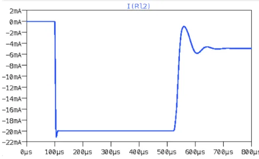
Figure5.17shows the load current transient waveform with a load of 500Ω, voltage output of 10V, and current limit of 2mA. Initially the load draws 20mA, as expected. A painfully long 400µs later, the current limiting circuit activates. After some minor overshoot ( 10%) it limits the currents to the specified 2mA. Even though this system is about 10 times slower than the voltage limiting system, it shows potential stability concerns.
Figure5.18below shows an even more frightening scenario. With a load of 500Ω, voltage output of -10V, and current limit of -5mA, the output current noticeably oscillates about 3 times before settling. The 25% overshoot is quite the scary sight, as is the 550µs response time. Nevertheless, the show must go on. In the SMU PCB layout unpopulated pads are left in case additional stabilizing components are needed.
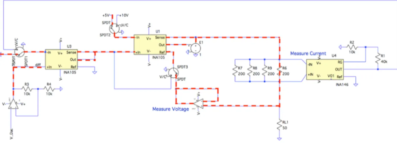
5.2.3 Revision C
The (hopefully)1 final revision of the SMU made a few changes to the output of the voltage source mode. In REV A, there is a 50Ω shunt resistance in series with the load. This resistance sets the current output when in current mode, but is useless in voltage mode. This resistance forms a voltage divider with the load leading to a decrease in the load voltage. Additionally, the 50Ω resistance burns 5W of power when the load draws a current of 100mA. The voltage drop nulling feedback loop discussed in REV A fixes the voltage drop problem, but is complicated and requires an additional relay. A solution for fixing both output impedance and power consumption problems is simply lowering the shunt resistance. A shunt resistance of 1Ω dissipate only 100mW at max current and alters the output voltage roughly 50 times less.
The problem with decreasing the shunt resistance is that it directly impacts the current output transfer function. The current output is given by equation3.
Iout=
V1−V2
Rshunt
(3)
With the new Rshunt of 1Ω and previous differential voltage of ±5V, the current output is now ±5A. The output buffer cannot supply this much current. The differential voltage must decrease to ±0.1V for a proper max output of ±100mA.
To reiterate, when in voltage mode,V1 varies from 0-10V,V2 is a constant 10V, which produces a -10V – 10V output. In current mode,V1 varies fromVref ± 0.1V,V2 is a constant VRef, which produces a -100mA – 100mA output when Rshunt is 1Ω.
The voltage at V2 is 10V when the SMU operates in voltage mode. If the differential voltage in current mode is 9.9V – 10.1V, the 10V reference doesn’t need adjustment. In REV A, a relay changed
V2 to 5V when in current mode. Revision C removes this relay, and uses fine and coarse control for the current/voltage adjustment. Two DACs have their voltages scaled and summed.
One DAC has its voltage (Vcoarse) produce an output of 0V – 10V, whilst the other produces DAC an output voltage (Vf ine) of -0.1V – 0.1V. These voltages sum and input to the voltage/current control input
V1. When in voltage mode Vf ine’s output contribution set to 0V and Vcoarse causes the output to vary between 0V – 10V, producing a total output of 0 – 10V. When in current modeVcoarse sets to the output to 10V and Vf ine contributes between -0.1V – 0.1V, producing a combined output of 9.9V – 10.1V.
Figure 5.19. Fine and Coarse Control Hardware Realization
Figure 5.19 shows the implementation of the functionality described above. The first block consisting of U1,R1-R4, and Vref scales and shifts theVf ine voltage. TheU2 and R5-R7 block sums the conditioned Vf ine and Vcoarse times 2. TheU3,R8,R9 inverts the voltage for an end result shown in equation 4.
V3 = 2∗Vcoarse+
Vf ine−2.5
25 (4)
When Vf ine andVcoarse vary from 0 – 5V, the appropriate voltages for control are produced.
An improvement to this design allows for the removal of an additional op-amp. Figure 5.20 shows a modified version with the same output voltage characteristics but with fewer components. This design was made after the SMU circuit board was ordered and is not on the Revision C schematic. The author recommends this improved design.
Figure 5.21. Output of Fine/Coarse Control for Voltage Mode
Figure 5.21 shows the output voltage when Vf ine is a constant 2.5V andVcoarse varies from 0-5V. The output varies from 0-10V.
Figure 5.22. Output of Fine/Coarse Control for Current Mode
Figure 5.22 shows the output voltage whenVcoarse is a constant 5V and Vf ine varies from 0-5V. The output varies from 9.9-10.1V.
5.3 Analog Input Output
5.3.1 Analog Input
The Analog Input and Outputs (AIO) are constrained mostly by the resolution specifications. The target voltage resolution is 100µV. A full scale range of ±10V calls for an 18-bit ADC/DAC. These ADC/DACs are typically slow; not a concern, but have an input/output range of 0 – 5V, which is. Bipolar to unipolar and unipolar to bipolar conversion techniques are needed to interface the systems to the outside world.
Figure 5.23. Input Circuity to the Analog to Digital Converter
The ADC chosen for the analog input is the ADS1220. This ADC is 24-bit, with up to 20 bits of effective resolution. This is more than the 18-bit needed for the target resolution. The ADS1220 has SPI communication and digital 50-60Hz rejection filters. For these reasons it is optimal for the analog input. The main drawback of the ADS1220 is that the input voltage range is 0 – 5V. The rest of the circuity shown in figure5.23 is signal conditioning and protection.
R1 and C1 form a low-pass filter. The purpose of this filter is to reduce the effects of aliasing on the output data. The cutoff frequency of this antialiasing filter is 1/RC, set at roughly the sampling rate (20Hz).
The bufferU1 (OPA4197) allows for a high impedance input. As a result, the analog input circuit does
not draw a significant current. The input bias current of the OPA4197 is 5pA typical and 20pA maximum (at TA = 25°C) 17.
The Differential-Impedance of the OPA4197 is 100MΩ. The voltage between the inputs is the output voltage divided by the DC gain (120dB). Equations5-7 the current drawn from the op-amp’s differential loading is at most 0.1pA. This current is negligible compared to input bias current.
Gain= 120dB= 1E6V /V (5)
V+−V−= 10V
Gain = 10µV (6)
The Common-Mode Impedance is 10E12Ω. This impedance is seen toward ground. Equation8shows the maximum current draw from the common mode loading is 1pA, occurring at the maximum input voltage of 10V. This current is comparable to the typical input bias current.
10V
10E12 = 1pA. (8)
Therefore, the total input current draw is roughly 21pA at worst, and is expected to be in the single digit picoamps during normal operation. This current draw is magnitudes lower than what is necessary to not load a typical undergraduate circuit.
The OPA4197 also has internal EMI protection which prevents ESD strikes and other overvoltage events from damaging the ADC. The anti-aliasing filter also protects the circuit from such events.
R2andR3 convert the bipolar signal (-10 – 10V) to a unipolar one (0 – 5V).2 The simple resistive divider
attenuates and DC offsets the oncoming signal. The resistor values are chosen to not load the buffer as well to not cause significant voltage error from the voltage divider with the ADC input. The ADC input is 100MΩ minimum18. The potential error caused by the loading of the ADC is 0.05%. This error is linear and is calibrated out. The R2,R3 resistor tolerance also contribute linear error; nothing to worry over.
5.3.2 Analog Output
Figure 5.24. Output Circuity for the Digital to Analog Converter
The Digital to Analog Converter (DAC) used is the MAX5134AGUE+. The output range is 0 – 5V, which needs to modified to meet the -5 – 5V and -10 – 10V output requirements. A INA145 difference amplifier converts the voltages to these ranges. Equation 9 shows the output voltage equation for a difference amplifier.
Vout= (Vin+−Vin−)∗Gain (9)
Figure 5.25. INA145 Adjustable Gain Difference Amplifier Design Recommendations 20
Figure 5.25 shows an excerpt from the The INA145 datasheet. The excerpt shows the gain equation and recommended resistor values. The datasheet also recommends that the parallel impedance of the gain setting resistors is equivalent to the R5 impedance (10kΩ). For a gain of 2, RG1 and RG2 values of 20kΩ
are used. For a gain of 5, RG2 is 40.2kΩ and RG1 is 13.3kΩ. This results in an equivalent resistance of
5.4 Digital Input Output
5.4.1 Digital Input
The Digital Input Output (DIO) specifications are fairly lax in comparison to the rest of the subsystems. To accommodate various logic families, adjustable VIL, VIH, VOL, VOH levels are needed. Despite the digital signal having an analog range of values, a full-fledged ADC is not necessary for the input. The digital inputs are built with a comparator and adjustable voltage threshold. The non-inverting terminal of the comparator is the input, and the inverting terminal is a variable threshold voltage. The threshold voltage would be the average of theVIL and VIH levels. Figure5.26 shows an example of this.
Figure 5.26. Graph Showing Threshold Voltage Set From Average of TTL Voltage Levels
Figure 5.27. Digital Input Structure with ESD/Overvoltage Protection
Figure 5.27shows the digital input circuit. D1 andD2 clamp the input voltage from roughly 0–5V. R1
limits the current flowing through the diodes. This prevents from any potential transient voltage spikes from reaching any internal circuity. R2 andC1 form a low-pass filter, reducing noise sensitivity and further protecting from voltage spikes. The LM339 (U1)is a cheap comparator.
5.4.2 Digital Output
Figure 5.28 shows the digital ouput circuit. The circuit is simply a voltage follower with an isolation resistor. The voltage follower boosts the maximum output current of the circuit. The resistor improves stability when driving capacitive loads. Again, DAC084S085 is used, for the same reasons as stated previously.
6 Testing
The proper method for inquiring after the properties of things is to deduce them from
experiments.
Isaac Newton
6.1 Power Supply
The Power Supply was the first subsystem tested, as such was approached with a very cautious optimism. It came as no surprise when the board didn’t work when first powered up. The current draw of the board was large, drawing over 500mA at 15V. A measurement of the REF5050 reference voltage showed a reading of 2V, indicating that the DAC was drawing substantial current. For testing purposes, a 5V power supply temporarily replaced the REF5050. When the DAC outputs are set to output 2.5V (mid-scale), pin 9 (AO6) remained at 5V. Coincidentally, pin 9 is next to the 5V power rail of the DAC. A continuity test confirmed that the two pins are shorted. After a quick solder cleanup, the DAC draws less than 10mA and has all outputs fully functioning.
The first test of a power supply is to characterize the voltage output under loading conditions. Each output is connected to a 330Ω resistive load, and had the output voltage monitored as a function of input code sent to the DAC. Table 6.1and figure6.1 show the relative error.
Figure 6.1. Power Supply Output vs Input Voltage
6.1.1 Line Regulation
Figure6.1shows the output voltages of each power supply vary linearly as a function of input code (set voltage). More interestingly, figure6.2shows the % voltage error at each output. After roughly 1V, the % error mainly resides in the ±0.5% range. This % error is a better specification than the original ±10mV spec. A ±10mV at a 12V output level is a relative % error of 0.083%, too stringent for the purpose of this project.
For reference, the Agilent E3631A has an output accuracy of ±(0.1% +5mV) on the 6V output 3. As this project likely has a much lower budget than that of Agilent’s, the power supply output accuracy specification is changed to ±(1.0% +5mV). The error bounds of the original and new specification are shown in figure6.3.
(a) New ±(1.0% +5mV) Accuracy Specification (b) Former ±10mV Accuracy Specification
Figure 6.3. Measured % Error plotted on same axis of Error Specifications
6.1.2 Load Regulation
The load regulation of the power supply is measured at an output voltage of 5V. The output voltage is monitored for a set of loads. Figure6.4shows the variation in load voltage for a range of resistive loads.
Figure 6.4. Variation in Output Voltage for Different Loads
Figure 6.5. Current Demand of Different Loads
The heaviest load draws 200mA, and the lightest drew 1mA. The open circuit voltage is 5.0088V, and the 200mA current draw load voltage is 4.9867V. Measurements are done with an Agilent 34401A Multimeter. Equations10 and 11 show the load regulation in percentage.
LoadRegulation(%) = Vmax−load−Vmin−load
Vnom ∗
100 (10)
0.422% = 5.0088−4.9867
6.1.3 Current Limiting
To the dismay of the author, each current shunt monitor needed calibration to accurately reflect the actual current delivered to the load. Figure 6.6shows this calibration process test setup.
Figure 6.6. Current Limit Calibration Setup
R1 is a potentiometer used to obtain different load currents. The load current is measured with an ammeter
and the current monitor is measured with a voltmeter. The output of the current monitor is fit to the measured load current. Figure6.7 shows the curve fit is linear, suggesting a simple gain and offset error.
Figure 6.7. Current Shunt Amp Output 2 For Selected Load Currents
Figure 6.8. Alert Voltage Triggering on Overcurrent Event
Figure 6.9. 100Ω Load with a 0–10V Step and 50mA Current Limit Load Voltage (Orange) and Alert (Green)
Figure 6.9shows the current limit response time with a 100Ω load on the output. When a 0–10V step is applied, the load draws 100mA. A current limit of 50mA is at set. The response time is measured from the time that the load voltage is at 5V (load draws 50mA) to the time the load voltage decreases back to 5V. The response time in this case is 50.9µs. While no current limit time specification is defined, a fast response time is desirable to prevent damage to circuity.
Upon close inspection, two distinct noise pulses are seen on the alert waveform at t = 32 and 40µs. These pulses are caused by the EMI generated from the SPI communication from the microcontroller writing to the DAC to reset its output. The pulses are absent from the load voltage as the PCB power planes are well bypassed.
The pulses are of interest because they show the relative timings of the current limiting process. From the alert negative edge to the SPI communication initiation is 34µs. This 34µs is the time it takes for the microcontroller to interrupt on the falling edge of the alert, clear the interrupt flag, and call a SPI function. The SPI communication takes roughly 8µs, during which 16 bits are transmitted. After the SPI communication ends, the DAC takes another 8µs to change its output. The datasheet value for the BU2507FV output settling time (7µs typical) verifies this value 26.
6.1.4 Transients
(a) 100Ω Load with a 0–10V Step
(b) 100Ω || 1µF Load with a 0–10V Step
(c) 100Ω || 10µF Load with a 0–10V Step
The power supply is subjected to a 0–10V input step under a set of loading conditions. Figure 6.10
shows the transient responses. Different load voltage slew rate and overshoots are seen based on the load capacitances. The slew rate of the power supply varied from 4V/µs to 0.08V/µs based on the capacitance present. The overshoot present suggests a damped response and therefore no stability concerns. All capacitors used were electrolytic, which have ESR values ranging from 1 – 100Ω at the capacitances and voltages tested29.
Figure 6.11. Power Supply Terminals Directly Shorted Transient
6.2 SMU
6.2.1 Early Prototype
As the first revision of the SMU showed promise, an early prototype is made. The prototype does not contain any relays; all connections are made manually. Figure 6.12 shows the bread-boarded prototype. This is the first circuit constructed during the course of the project.
Figure 6.12. SMU Early Prototype on Breadboard
The circuit is crude: the reference voltages are generated from resistive dividers, and potentiometers mimic the DAC output voltages. Nevertheless, the circuit works as intended and proves its viability. Figure
(a) Voltage Output
(b) Current Output
Figure 6.13. Voltage and Current Transfer Characteristics of Proto-SMU
6.2.2 Voltage Mode
Figure 6.14. SMU Voltage Transfer Characteristic
Figure 6.14 shows the input vs no-load output voltage. Figure 6.15 shows the % error of the voltage output. The SMU voltage output meets the original specification of ±10mV. Nevertheless, an updated specification is preferred for some margin. Equation 12 shows the new specification. Figure 6.15a shows the original specification. Figure 6.15bshows the new error bounds.
% Error Bounds=±(0.5% + 5mV) (12)
(a) Original Error Specification (b) Updated Error Specification
(a) +10V Output Load Regulation (b) +5V Output Load Regulation
(c) -10V Output Load Regulation (d) -5V Output Load Regulation
Figure 6.16. Load Regulations for Selected Output Voltages
Figure 6.16 show the SMU’s load regulation for four output voltages. A load of 100Ω is the heaviest load tested. This load draws 100mA when attached to the ±10V outputs and 50mA for the ±5V outputs. Figure 6.17 show the % error of the outputs. Each of the four output voltages follow the same % error trend, indicating a constant output impedance. Equation 13 shows the formula used to calculate output impedance.
Output Impedance= Vopen−circuit∗Load Resistance
Vloaded −
Load Resistance (13)
From equation 13, the output impedance of the SMU averages to 1.36Ω. Figure 6.18 shows the main potential sources of output resistances.
Figure 6.18. Resistors in Output Signal Path
Because the shunt resistor is 1Ω, the rest of the resistances sum to 360mΩ. The trace resistance is estimated to be roughly 10mΩ. This estimate comes from the trace width (7.62mm), trace thickness (2.8 mil), and trace length ( 30mm). The output resistance of the OPA633 is 5Ω typical 27. However, the output resistance is seen in a feedback path and is nullified as a result. The relay resistance is 150mΩ max. This leaves 200mΩ likely present from the MOSFETS. The MOSFETs are chosen for their lowRDS−on24,
6.2.3 Current Mode
Figure 6.19. SMU Current Transfer Characteristic
Figure 6.19 shows the input vs output current. Figure 6.20 shows the % error of the voltage output. The SMU current output is close, but does not meet the original specification of ±0.1mA. Equation 14
shows an updated specification. Figure6.20ashows the original specification. Figure 6.20bshows the new error bounds.
% Error Bounds=±(0.5% + 25A) (14)
(a) Original Error Specification (b) Updated Error Specification
An astute reader may notice that the bottom left most datapoint in figure 6.19 doesn’t follow the trendline. This is because the calibrated code sent to the DAC is less than zero. The solution to this problem is to simply adjust the Vcoarse DAC output upward by a few codes. This shifts the current transfer characteristic downward, allowing for the utilization of the full range. Figure 6.21 shows the zoomed out % error plots containing the erroneous datapoint.
Figure 6.21. % Error of Current Mode (Zoomed Out View)
6.3 AIO
6.3.1 Analog Output
The analog output circuit has 4 different channels. Two channels output voltage from -10–10V, and the other two output -5–5V. Each channel needs calibration to account for various error sources in the system. Among these error sources are DAC offset and gain error, op-amp offset voltage, and gain setting resistor tolerance. Nullification of these errors is done with equations or look-up tables.
The main error sources affect either offset or gain of the output transfer function. These error terms are linear and are calibrated with a simple y = mx + b equation. A look-up table are used if more complicated errors are present (DAC integral non-linearity, for example).
Figure 6.22. % Error Before and After Calibration (Output Channel 3)
After calibration the average magnitude of the error improved by a factor of 22.79. Additionally, the calibrated error now fits within error bounds of ±(0.1% + 1mV). The author deems this percent error impressive for a system with no feedback or other control circuity. The advantage of reaching such low error without feedback is that there are no stability concerns. Additionally, control circuity increases cost and board complexity.
Not all calibrations resulted in such a drastic improvement. Figure6.23 shows the output error before and after calibration of analog output channel 0 as a function of full scale range percentage.
Figure 6.23. % Error Before and After Calibration (Output Channel 0)
6.3.2 Analog Input
The calibration process for the analog input is arduous. The ADC has 24 output bits, which correspond to a resolution of 1.192µV. Special measurement conditions are made when dealing with such a small voltage resolution. The Agilent 34401A 6½ digit multimeter has its terminals shorted for nulling out any offset. Multimeter measurements are averaged after given roughly 20 seconds to settle. The measurements the analog input takes are also averaged. The analog input takes the 8 most recent readings for its average. With these simple techniques, precise measurements are made.
The project’s analog output feed into the analog input and the multimeter probe. At some points in time, this project has the capability to test itself. The author of this project shed a single tear of pride at the mere thought of this.
Figure 6.24. % Error with Zero, One, and Two Calibration Passes (Input Channel 3)
The analog input requires about 2-3 linear calibrations passes before acceptable results are seen. Eventually no notable improvement results from repeated calibrations. Figures 6.24 and 6.25 show the improvement calibration made. For reference, equation 15 shows the gain/offset correction equation for analog input channel 3.
voltage=reading∗1.00368548 + 0.0285495; (15)
Each of the significant figures in equation15 is relevant. A change in the last figure of the offset term results in hundreds of nanovolts of error. A change in the last figure of the linear term results in microvolts of error when at the maximum input voltages. Figure 6.26 show the happy consequences of such a tight calibration.
Figure 6.26. % Error After Two Calibrations with Error Bounds (Input Channel 3)
Equation 16shows the error specification of the Analog input.
6.4 DIO
6.4.1 Digital Output
The digital outputs did not require strenuous testing. Calibration even is forgone in pursuit of testing other subsystems. Nevertheless, some data is collected.
Figure 6.27. Output Voltage Transfer Characteristics of Digital Outputs
Figure6.27 shows the output voltage transfer characteristic of three of the four digital outputs. Unfor-tunately digital output channel 0 burned out after it was shorted to 5V in a soldering mishap.
Figure 6.28. % Error of Digital Outputs
Figure 6.29 shows the 90%-10% fall time of digital output channel 1. Unfortunately, the specified fall time of 1µs isn’t met. Although this isn’t a primary concern, a potential fix is identified and detailed in the errata section of the report.
6.4.2 Digital Input
Testing the digital inputs is a simple task. A 10kHz 1Vpp sine wave with a 2.5V is input into a digital input channel. The VIL and VIH are configured to achieve a trip voltage of 2.5V. Figure 6.30 shows the sine wave input and square wave output. The square wave output has roughly 50% duty cycle as expected. Propagation delays of about 7-10µs are seen. These delays are from the filter on the input and the innate propagation delay of the comparator.
Figure 6.30. Input (Orange) and Output (Green) of Digital Input withVtrip set to 2.5V
Figure6.31 shows the effect of the RC input filter on the digital input. A 5kHz 0-5V square wave input results in a rounded output. The main purpose of the RC filter is to help protect the input from high frequency noise.
Figure 6.32shows the effect of the overvoltage protection circuit. A 500Hz 10Vpp sine wave with a 2.5V offset is fed into the digital input. The voltage measured at the comparator input is clamped at -0.8V and 5.8V.
7 Conclusion
I am somewhat exhausted; I wonder how a battery feels when it pours electricity into a
non-conductor?
Arthur Conan Doyle
The author (from here on out referred to in the first person) believes this project was a success. Initially I had no clue how I was going to get any of the subsystems working. Through a lot of research, I slowly started to get an idea for the analog inputs and outputs. I went though many revisions based on of the fact that most DACs and ADCs don’t interface with the voltages I wanted to allow. I was most afraid of the SMU. The SMU was broken down into different sections. First the current mode worked, and then the voltage mode worked. I built a prototype just to make sure my simulations were working correctly. Once that was verified, the voltage/current limiting was added. This took a painfully long time. I remember seeing a square wave, triangle wave, and sine wave at different nodes of the SMU circuit (after a step input was applied).
Figure 7.2. Lest anyone want to attempt to tame the Hell Circuit
Fortunately, the power supply was a pleasure to make after the SMU insanity. The board designs were fun to do, as was collecting quotes for the PCB/report. Testing the power supply was the most fun I had with circuits for a long time. Once it was working (which was not trivial in the slightest) I was burning resistors and LEDs just to see the magic smoke pop out without me freaking out for once. I tested the overcurrent protection by licking the leads.
The analog input and outputs were a massive pain to calibrate without automation, but once I did I couldn’t believe the accuracy. I remember my phone died so I asked a random person to take a picture of the bench multimeter and my input and output reporting the same voltage down to the 100s of microvolt and better. The AIO section of the AIO/DIO board is what I am most proud of.
8 Errata
Look, what do mistakes do but just extend the pleasure of building?
Adam Savage
8.1 Power Supply
The power supply has one (known) mistake. The pin-out of the NPN/PNP is incorrect. The library symbol had a pinout commonly used by the TO-92 package. The actual package used is the TO-220, chosen for better power dissipation. The TO-92 symbol used had a pinout of E-B-C (C-B-E for PNP), while the TO-220 part ordered has a pinout of B-C-E. Figure 8.1 shows the incorrect schematic in 8.1a
and 8.1cand the corrected version in 8.1b and8.1d.
(a) Incorrect Pinout for NPN Transistor (b) Correct Pinout for NPN Transistor
(c) Incorrect Pinout for PNP Transistor (d) Correct Pinout for PNP Transistor
Power Supply Revision B corrects the issue. The author opts to bend the transistor leads to the correct orientation over ordering a entirely new PCB. Figure 8.2shows the bent leads. The author refers to this shape as an aesthetically pleasing coalescence of the old (Romans) and the new (Transistors). The Museum of Modern Art has not returned the author’s calls.
Figure 8.2. Roman Numeral Realization in Hardware
8.2 SMU
The SMU revision C schematic contains (quite) a few errors. The DAC used for the voltage control is powered with a 5V reference voltage. However, the internal 2.5V reference is used as it’s reference. The author forgot that this would limit the DAC output to 2.5V. A simple fix is to double the gain/half the attenuation in the voltage conditioning circuits. Table ??shows resistors with changed values.
Another issue with the SMU is with the coarse fine control. As the maximum voltage produced from the coarse control is 10V, any resistor tolerances/DAC max output error may reduce the actual voltage. The SMU in current mode is relatively sensitive to voltage errors; with an offset of just 10mV results in a current error of 10mA. To remedy this, the resistors are modified slightly in order to allow for some slack. This slack means that the fine/coarse outputs produces larger voltage swings than needed. This, along with calibration, compensates for any tolerance/DAC errors. Table 8.1 shows resistors modifications made during testing. Figure 8.4shows the DAC voltage conditioning circuits in Revision D.
Table 8.1. Resistor Changes Made to SMU Rev C
Resistor Previous Value New Value
R9 10kΩ 5kΩ
R12 20kΩ 10kΩ
R13 20kΩ 15kΩ
R16 10kΩ 5kΩ
R20 50kΩ 10kΩ
The op-amp used for the voltage limit has it’s input terminals swapped. Figure8.5 show the incorrect and correct configurations.
(a) Incorrect Input Terminals (b) Correct Input Terminals
Figure 8.5. A Fun Game of Spot the Difference
There are a few silkscreen mistakes throughout the project. However, most of the mistakes are minor; only affecting the legibility of the designator. Figure8.6ashows the one instance of an incorrect designator. The R9 and R10 silkscreen locations are swapped. In figure 8.6bthe R9 designator correctly refers to the upper resistor.
(a) Incorrect Reference Designator (b) Correct Reference Designator
From the OPA633 datasheet:
”Pin 6 connects to the substrate of the integrated circuit and should be connected to ground. In principle it could also be connected to +VS or –VS, but ground is preferable.” 27
8.3 AIO
Due to resistor tolerance, the output voltage can not reach the full scale output endpoints. The gain of the analog output is too low. A fix to this problem is to use resistor values that give gain above 2. Another more involved fix is measuring the exact resistor values and placing them to ensure the gain is greater than 2. The probability of a gain less than 2 occurring is 50%. This would be devastating in a production environment and revisal is imperative. This problem is less likely to occur in the ±10V outputs as the resistors set the ideal gain to 4.02. When worst case tolerances are taken into account, the gain of the output is 3.96, less than 4. A MATLAB script finds the probability of the actual gain is less than 4 when 1% tolerance resistors are used.
Figure 8.7. Gain as a Function of 2 Resistor Tolerance Ranges
8.4 DIO
The digital output circuit did not meet the spec’d rise/fall time of 1µs (with load of 2000kΩ || 1000pF). While this doesn’t concern the author in the slightest, the problem is analyzed.
8.5 µC Board
The linear regulator ordered is incorrect. An adjustable output component was ordered instead of a 5V variant. feedback resistors set the output voltage to approximately 5V.
(a) Incorrect Orientation (b) Correct Orientation
Figure 8.8. The Results of Two Hours of Soldering
The relays on the µC board are flipped. Figure8.8 shows the schematic fix.
9 Appendices
People think that mathematics is complicated. Mathematics is the simple bit, it’s the stuff we CAN understand.
It’s cats that are complicated.
John Conway
9.1.4 SMU Revision D 1 2 3 4 5 6 1 2 3 4 5 6
A B C D
A B C D
Date:
KiCad E.D.A. kicad (5.1.4-0)
Rev: Size: A4 Id: 1/5 Title: File: SMU_Rev_D.sch Sheet: /
Sheet: relay_drivers File: relay_drivers.sch Sheet: ADC File: ADC.sch Sheet: voltage_references File: voltage_references.sch Sheet: DAC File: DAC.sch
0
1 2 3
J6 Screw_Terminal_01x03
1 2 3
J4 Screw_Terminal_01x03
0
0
0
1 2 3
J3 Screw_Terminal_01x03 0 C34 0.1u 0 C33 0.1u 0 0
1 2 3 4 5 6
J5 Conn_01x06
0
1 2 3 4 5 6
J2 Conn_01x06 + 11 4 OUT 1 -IN 2 +IN 3 U7A OPA4141 + 11 4 OUT 1 -IN 2 +IN 3 U4A OPA4197 2 6 +IN 3 -IN 4 OUT 5 U5B LT1126 + 2 6 +IN 1 OUT 7 -IN 8 U5A LT1126 +Vs 1 In 4 -Vs 5 Sub 6 Out 8 U2 OPA633 Ref 1 -IN 2 +IN 3 V- 4 Sense 5 Out 6 V+ 7 U1 INA105 Ref 1 -IN 2 +IN 3 V- 4 Sense 5 Out 6 V+ 7 U3 INA143 0 C3 1u 0 C6 1u R1 150 0 C11 DNP R3 10k C8 330p 0 0 C14 DNP 1 2 J1 Conn_01x02 R4 10 0 R2 1 0 C4 0.1u 0 C2 0.1u 0 C5 1u 0 D1 1N4148 D2 1N4148 C1 1u 0 C10 0.1u 0 C12 0.1u 0 C9 0.1u 0 C7 0.1u 0 S 1 2 3 G
4
D 5 6 7 8 Q4 DMT6010LSS-13
S 1 2 3 G
4
D 5 6 7 8
Q3
AO4447A
S 1 2 3 G
4
D 5 6 7 8 Q2 DMT6010LSS-13
R5 10k S
1 2 3 G
4
D 5 6 7 8
1 2 3 4 5 6 1 2 3 4 5 6
A B C D
A B C D
Date:
KiCad E.D.A. kicad (5.1.4-0)
Rev: Size: A4 Id: 2/5 Title: File: DAC.sch Sheet: /DAC/ OUT_A 1 SCLK 10 DIN 11 D_VDD 12 RST 13 RSTSEL 14 EN 15 LDAC 16 OUT_B 2 V_REF_H 3 A_VDD 4 V_REF_L 5 GND 6 OUT_C 7 OUT_D 8 SYNC 9 U6 DAC7565 R14 10k 11 4 +IN 5 -IN 6 OUT 7 U7B OPA4141 + 11 4 +IN 5 -IN 6 OUT 7 U4B OPA4197 C15 150n 0 C17 0.1u C16 1u + 11 4 +IN 10 OUT 8 -IN 9 U4C OPA4197 R15 10k R16 30.1k 0 R9 10k R11 75k R10 10k 0 R13 1k R8 1k
R7 100k R12 49.9k 0
1 2 3 4 5 6 1 2 3 4 5 6
A B C D
A B C D
Date:
KiCad E.D.A. kicad (5.1.4-0)
Rev: Size: A4 Id: 3/5 Title: File: voltage_references.sch Sheet: /voltage_references/ C35 4.7u C19 4.7u C18 4.7u 0 0 0 Vin 2 Temp 3 GND 4 Trim/NR 5 Vout 6 U9 REF5050AD 0 C27 4.7u 0 C20 1u
C23 4.7u 0
0
C28 1u
0
C24
4.7u
C21 4.7u 0
C22 4.7u Vin 2 Temp 3 GND 4 Trim/NR 5 Vout 6 U8 REF5010AD 0 C30 1u R22 1 C29 1u 0 C25 1u
R21 1 C26 1u
1 2 3 4 5 6 1 2 3 4 5 6
A B C D
A B C D
Date:
KiCad E.D.A. kicad (5.1.4-0)
1 2 3 4 5 6 1 2 3 4 5 6
A B C D
A B C D
Date:
KiCad E.D.A. kicad (5.1.4-0)
Rev: Size: A4 Id: 5/5 Title: File: relay_drivers.sch Sheet: /relay_drivers/ D6 1N4148 D5 1N4148 R34 10k D4 1N4148 0 1 13 14 2 6 7 8 9 K2 HE721C0500 1 13 14 2 6 7 8 9 K4 HE721C0500 R33 10k D3 1N4148 1 2
3 Q5 2N3904 1 13 14 2 6 7 8 9 K1 HE721C0500 1 2
3 Q6 2N3904 1
2
3 Q8 2N3904
0 R36 10k 1 13 14 2 6 7 8 9 K3 HE721C0500 1 2
3 Q7 2N3904
1 2 3 4 5 6 1 2 3 4 5 6
A B C D
A B C D
Date:
KiCad E.D.A. eeschema (5.1.4-0)
Rev: Size: A4 Id: 5/5 Title: File: Digital_Output.sch Sheet: /Digital_Output/ R21 5 0 0 C23 0.1u 0 C25 0.1u V- 11 V+ 4 U10E TLV3544 OUT 1 IN-2 IN+ 3 U10A TLV3544 IN+ 10 OUT 8 IN-9 U10C TLV3544 IN+ 12 IN-13 OUT 14 U10D TLV3544 0 VA 1 SCLK 10 VOUT_A 2 V_OUT_B 3 V_OUT_C 4 V_OUT_D 5 GND 6 V_REF 7 DIN 8 SYNC 9 U11 DAC084S085 R22 5 IN+ 5 IN-6 OUT 7 U10B TLV3544 R24 5 R23 5 DOUT2 DOUT3 DOUT1 DOUT0 +5V D_OUT_0 +5V DOUT0 DOUT3 DOUT2 D_OUT_2 DOUT1 D_OUT_1 +5V
CLK DAC_D_OUT_CS DATA

![Figure 5.1. Functional Block Diagram of the LM317 in Adjustable Voltage Regulator Configuration [16]](https://thumb-us.123doks.com/thumbv2/123dok_us/8221704.2179752/32.918.138.752.264.781/figure-functional-block-diagram-adjustable-voltage-regulator-configuration.webp)