DC-DC Energy Conversion with Novel loaded Resonant
Converter
Chiranjeevi Garapati1, Sk Gouse Basha2, Ravikumar Reddy P3
1*Pursuing M.Tech in the field of Power Electronics, NCET, Vijayawada, AP, India 2*Working as, Assistant professor in the EEE Dept, NCET, Vijayawada, AP, India 3*Pursuing M.Tech in the field of Power & Industrial Drives, NCET, Vijayawada, AP, India
ABSTRACT:
This paper presents the direct current (dc)-to-dc energy conversion with novel loaded-resonant converter. Energy shortages and increasing oil prices have created the demand for a high energy conversion efficiency and performance. The growing electronic product market has increased the demand for high energy conversion efficiency and high power density of dc-to-dc energy power converters. The soft switching scheme is the most attractive dc-to-dc energy conversion topology in recent years. The soft-switching method can reduce switching losses and EMI of the switch-mode converter. Among the many advantages that resonant power conversion has over conventionally adopted pulse-width modulation include a low electromagnetic interference, low switching losses, small volume, and light weight of components due to a high switching frequency, high efficiency, and low reverse recovery losses in diodes owing to a low di/dt at switching instant. The proposed topology comprises a half-bridge inductor-capacitor inductor (L-C-L) resonant inverter and a bridge rectifier. Output stage of the proposed loaded-resonant converter is filtered by a low-pass filter. A prototype dc-to-dc energy converter circuit with the novel loaded-resonant converter designed for a load is developed and tested to verify its analytical predictions. The measured energy conversion efficiency of the proposed novel loaded-resonant topology reaches up to 88.3%. Moreover, test results demonstrate a satisfactory performance of the proposed topology. Furthermore, the proposed topology is highly promising for applications of switching power supplies, battery chargers, uninterruptible power systems, renewable energy generation systems, and telecom power supplies. The experimental results are clearly verified by simulation results.
1. INTRODUCTION:
A DC-to-DC converter is an electronic circuit which converts a source of direct current (DC) from one voltage level to another. It is a class of power converter. Use of semiconductor power switches in power electronic technology has led to rapid development of this technology in recent years. The switching power converter plays a significant role in the power energy conversion applications. In particular, direct current (dc)-to-dc converters are extensively adopted in industrial,
commercial, and residential equipment. These converters are power electronics circuits that convert a dc voltage into a different level, often providing a component of power energy conversion systems. Pulse-width modulation (PWM) is the simplest way to control power semiconductor switches. The PWM approach controls power flow by interrupting current or voltage through means of switch action with control of duty cycles. In practice, a situation in which the voltage across or current through the semiconductor switch is abruptly interrupted is referred to as a hard-switched PWM. Because of its simplicity and ease in control, hard switched PWM schemes have been largely adopted in modern power energy conversion applications.
Several methods exist to achieve DC-DC voltage conversion. Each of these methods has its specific benefits and disadvantages, depending on a number of operating conditions and specifications. Examples of such specifications are the voltage conversion ratio range, the maximal output power, power conversion efficiency, number of components, power density, galvanic separation of in- and output, etc. When designing fully-integrated DC-DC converters these specifications generally remain relevant, nevertheless some of them will gain weight, as more restrictions emerge. For instance the used IC technology, the IC technology options and the available chip area will be dominant for the production cost, limiting the value and quality factor of the passive components. These limited values will in-turn have a significant impact upon the choice of the conversion method. Energy shortages and increasing oil prices have created the demand for a high energy conversion efficiency and performance. The growing electronic product market has increased the demand for high energy conversion efficiency and high power density of dc-to-dc energy power converters. The soft switching scheme is the most attractive dc-to-dc energy conversion topology in recent years.
II. PROPOSED SYSTEM DESCRIPTION
& ITS OPERATING PRINCIPLE:
1. Resonant Converters:
Description: Resonant power converters contain resonant L-C networks whose voltage and current waveforms vary sinusoidally during one or more subintervals of each switching period. These sinusoidal variations are large in magnitude, and the small ripple approximation does not apply.
Some types of resonant converters: 1. Dc-to-high-frequency-ac inverters 2. Resonant dc-dc converters
3. Resonant inverters or rectifiers producing line-frequency ac
Fig 1: Switching circuit of resonant converter Several resonant tank networks
Fig 2: Several resonant tank networks Advantages:
1. The chief advantage of resonant converters: reduced switching loss
a. Zero-current switching b. Zero-voltage switching
2. Turn-on or turn-off transitions of semiconductor devices can occur at zero crossings of tank voltage or current waveforms, thereby reducing or
eliminating some of the switching loss mechanisms. Hence resonant converters can operate at higher switching frequencies than comparable PWM converters
3. Zero-voltage switching also reduces converter-generated EMI
4. Zero-current switching can be used to commutate SCRs
5. In specialized applications, resonant networks may be unavoidable,
a. High voltage converters: significant transformer leakage
b. Inductance and winding capacitance leads to resonant network
Dis-advantages:
1. Can optimize performance at one operating point, but not with wide range of input voltage and load power variations
2. Significant currents may circulate through the tank elements, even when the load is disconnected, leading to poor efficiency at light load
3. Quasi-sinusoidal waveforms exhibit higher peak values than equivalent rectangular waveforms 4. These considerations lead to increased conduction
losses, which can offset the reduction in switching loss
5. Resonant converters are usually controlled by variation of switching frequency. In some schemes, the range of switching frequencies can be very large 6. Complexity of analysis
2. DC-DC Converter:
Introduction: A DC-to-DC converter is an electronic circuit which converts a source of direct current (DC) from one voltage level to another. It is a class of power converter. Use of semiconductor power switches in power electronic technology has led to rapid development of this technology in recent years. The switching power converter plays a significant role in the power energy conversion applications. In particular, direct current (dc)-to-dc converters are extensively adopted in industrial, commercial, and residential equipment. These converters are power electronics circuits that convert a dc voltage into a different level, often providing a component of power energy conversion systems. Pulse-width modulation (PWM) is the simplest way to control power semiconductor switches. The PWM approach controls power flow by interrupting current or voltage through means of switch action with control of duty cycles. In practice, a situation in which the voltage across or current through the semiconductor switch is abruptly interrupted is referred to as a hard-switched PWM. Because of its simplicity and ease in control, hard switched PWM schemes have been largely adopted in modern power energy conversion applications.
Fig 3: Typical switching trajectories of power switches A higher switching frequency implies smaller and lighter inductors, capacitors, as well as filter components of these converters. However, electromagnetic interference (EMI) and switching losses increase with an increasing switching frequency, ultimately decreasing the efficiency and performance of dc-to-dc power converters. To solve this problem, some soft switching approaches must operate under a high switching frequency. Zero voltage switched and zero current switched schemes are two commonly used soft switching methods, in which either the voltage or current is zero during switching transitions, which largely reduce the switching losses, EMI, and increase the reliability of the power converters. While attempting to devise dc-to-dc converters capable of operating at low switching losses, power electronics engineers started developing converter topologies that shape either a sinusoidal current or a sinusoidal voltage waveform, regulated output. Power semiconductor switches are the major significantly reducing switching losses. Such converters are called soft switching dc-to-dc converters. A soft switching dc-to-dc converter is constructed by cascading a resonant dc-to-alternating current (ac) inverter and a rectifier. DC input power is first converted into ac power by the resonant inverter; the ac power is then converted back into dc power by the rectifier. Among the existing soft switching converters, loaded-resonant converters are the most popular type owing to its simplicity of circuit configuration, easy realization of control scheme, low switching losses, and high flexibility for energy conversion applications.
Depending on how energy is extracted from a resonant tank, loaded-resonant converters can be classified into series resonant, parallel resonant and series-parallel resonant converters. The series resonant charger is normally formed by an inductor, capacitor, and bridge rectifier. The ac through the resonant tank is rectified at the output terminals, making it possible to obtain the output dc. In contrast to the series resonant converter, the parallel loaded- resonant converter can control the output voltage at no load by running at a frequency above resonance. The parallel loaded-resonant converter contains an inductive output filter, explaining why the output current through the capacitor is low and reducing the conduction losses and the ripple voltage of the converter. Furthermore, the parallel-loaded-resonant converter is inherently short circuit
protected. Hence, the parallel-loaded resonant converter is highly promising for dc-to-dc energy conversion applications. Notably, the output voltage at resonance is a function of load and can rise to very high values at no load if the operating frequency is not raised by the regulator. However, the series-parallel converter integrates the best characteristics of series resonant and parallel resonant converters. The resonant tank of this converter is equivalent to that of the parallel loaded-resonant inverter, except for an additional capacitor in series with the resonant inductor. The series-parallel converter output can run over a wider input voltage and load ranges from no load to full load. For the series-parallel converter with a capacitive output filter, analyzing converter operations and designing circuit parameters are complex tasks because the capacitive output stage is decoupled from the resonant stage for a significant period during the switching cycle. Additionally, the series-parallel converter cannot operate safely with a short circuit at a switching frequency close to the resonant frequency. Therefore, the energy conversion stage of the series-parallel converter has not been minimized and simplified, resulting in a bulky size and high cost in the applications of dc-to dc energy conversion. Comparing the above three different loaded-resonant converter topologies reveals that the parallel loaded- resonant converter is the optimum topology for dc-to dc energy conversion applications because of its many merits including low switching losses, low stresses, and low noise characteristics. Moreover, for dc-to-dc energy conversion applications, the parallel-loaded-resonant converter is generally recommended as the energy conversion stage due to its simple circuitry and typical input characteristics. However, a large filter inductor to the output side of the bridge rectifier in a traditional parallel-loaded-resonant converter might add significant weight, volume, and cost. Based on the parallel-loaded resonant converter, this work presents a novel loaded-resonant converter. The proposed novel loaded-resonant converter is superior to the conventional parallel resonant converter in terms of miniaturize size, light weight, simple topology, and easy control.
Circuit Diagram:
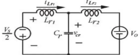
Circuit Description: Energy shortages and increasing oil prices have created the demand for a high energy conversion efficiency and performance. The growing electronic product market has increased the demand for high energy conversion efficiency and high power density of dc-to-dc energy power converters. The soft switching scheme is the most attractive dc-to-dc energy conversion topology in recent years. The soft-switching method can reduce switching losses and EMI of the switch-mode converter. Fig. 4 shows the proposed loaded-resonant converter for application of the dc-to-dc energy conversion system. The two capacitors, C1 and C2, on the input are large and split the voltage of the input dc source. The elementsLr1,Lr2, andCrform the resonant tank. The load resistanceRis connected across a bridge rectifier via a low-pass filter capacitorCo. For analysis, the power switching devices are assumed here to be represented by a pair of bidirectional switches operating at a 50% duty ratio over a switching periodT. For the half-bridge topology, each bidirectional power switch has an active power switch and an anti parallel diode. The active powers switches are driven by non overlapping rectangular-wave trigger signals vGS1 and vGS2 with dead time.
Thus, we may represent the effect of the power switches by means of an equivalent square wave voltage source with an amplitude equal to Vs/2. Resonant inductor currentiLr2 is rectified to obtain a dc bus. The dc bus voltage can be varied and closely regulated by controlling the switching frequency. Because of that, the ac-to-dc power conversion, in this case, is achieved by rectifying the current through resonant inductor Lr2, a large filtering capacitance Co is needed not only to minimize the loading effect of the output circuit, but also to ensure that the voltage across it is mostly constant. Consequently, the voltage across the bridge rectifier has constant amplitudes +Vo and −Vo, depending on whether the currentiLr2 (t) is positive or negative, respectively. The frequency of this voltage waveform is the same as that of the switching frequency. Based on the above observations, the novel loaded-resonant converter can be modeled as a series Lr1 − Cr − Lr2 circuit and a square-wave voltage source }Vo in series with the resonant inductor Lr2. Fig. 5 shows the simplified equivalent circuit for the proposed loaded-resonant converter.
Fig 5: Simplified equivalent circuit of the proposed loaded-resonant converter
Operating Principle: The following analysis assumes that the converter operates in the continuous conduction mode, in which the semiconductors have ideal
characteristics. Fig. 6 displays the idealized steady state voltage and current waveforms in the proposed novel loaded-resonant converter for a switching frequency fs that exceeds resonant frequency fo. Operating above resonance is preferred because the power switches turn on at zero current and zero voltage; thus, the freewheeling diodes do not need to have very fast reverse-recovery characteristics. During the positive half-cycle of the current through the resonant inductor Lr2, the power is supplied to the load resistor R through diodes DR1 and DR2. During the negative half-cycle of the current through the resonant inductor Lr2, the power is fed to the load resistor R through diodes DR3 and DR4.
Fig 6: Idealized voltage and current waveforms The novel loaded-resonant converter for the application of dc-to-dc energy conversion is analyzed based on the following assumptions.
1) Switching elements of the converter are ideal, such that the decline in forward voltage in the on-state resistance of the power switch is negligible;
2) Equivalent series resistance of the capacitance and stray capacitances is negligible;
3) Characteristics of passive components are assumed to be linear, time invariant, and frequency independent;
4) Filter capacitorCo at the output terminal of the full bridge rectifier is usually very large; the output voltage across capacitor Co can thus be treated as an ideal dc voltage in each switching cycle; and
Steady-state operations of the novel loaded-resonant converter in a switching period can be divided into four modes.
Mode I: (Between ωot0 and ωot1):
Periodic switching of the resonant energy tank voltage between +Vs/2 and −Vs/2 generates a square-wave voltage across the input terminal. Since the output voltage is assumed to be a constant voltageVo, the input voltage to the full-bridge rectifier isVowheniLr2 (t) is positive and is −Vo when iLr2 (t) is negative. Hence, below fig displays the equivalent circuit of the proposed novel loaded resonant converter for the application of dc-to-dc energy conversion in Fig 4. This time interval ends when iLr2 (t) reaches zero at ωot1. Before ωot0, active power switch S2 is excited and conducts a current that equals resonant tank current iLr1. The active power switch S1 is turned on at ωot0. However, resonant tank current iLr1 is negative and flows through freewheeling diode D1. At instant ωot1, resonant tank current iLr1 reverses and naturally commutates from freewheeling diode D1 to power switch S1. In this mode, the power switches are turned on naturally at zero voltage and at zero current. Therefore, the current through the active power switch is negative after turning on and positive before turning off. Although the current in the switches is turned on at zero voltage and zero current to eliminate turn-on losses, the switches are forced to turn off a finite current, thus allowing turn-off losses exit. Fortunately, small capacitors can be placed across the switches to function as snubbers in order to eliminate turnoff losses.
Mode II: (Between ωot1 and ωot2):
The cycle starts at ωot1 when the current iLr1 resonant tank resonates from negative values to zero. At ωot2, before the half-cycle of resonant current iLr1 oscillation ends, switch S1 is forced to turn off, forcing the positive current to flow through bottom freewheeling diode D2. Below fig. shows the equivalent circuit. The positive dc input voltage applied across the resonant tank causes the resonant current that flows through the power switch to go quickly to zero.
Mode III: (Between ωot3 and ωot4):
A turn-off trigger signal is applied to the gate of the active power switch S1. The inductor current then
naturally commutates from active power switch S1 to freewheeling diode D2. Mode III begins atωot3, when diode D2 is turned on, subsequently producing a resonant stage between inductorsLr1,Lr2 and capacitor Cr. InductorsLr1,Lr2, and capacitorCrresonate. Before ωot4, trigger signalvgs2 excites active power switchS2. This time interval ends when iLr1 (t) reaches zero at ωot4. Fig. 7 shows the equivalent circuit.
Mode IV: (Between ωot4 and ωot5):
When capacitor voltage iLr2 is positive, rectifier diodes DR1 and DR2 are turned on with zero-voltage condition at instant ωot4. Below figure shows the equivalent circuit. When inductor current iLr2 changes direction, rectifier diodes DR1 and DR2 are turned off at instant ωot5, and Mode IV ends. When driving signalVgs1 again excites active power switchS1, this mode ends and the operation returns to mode I in the subsequent cycle. During the positive half-cycle of the inductor currentiLr2, the power is supplied to the load through bridge rectifier diodesDR1 andDR2. During the negative half-cycle of the inductor current, the power is supplied to the load through bridge rectifier diodesDR3 andDR4.
Operating Characteristics:
the power of the fundamental component is transferred from the input source to the resonant circuit. Hence, it is sufficient to consider only the fundamental component of this converter. The novel loaded-resonant converter with a bridge rectifier stage for dc-to-dc energy conversion system is analyzed by considering the fundamental frequency of the Fourier series for the voltages and currents. The error due to this approximation is rather small when the switching frequency is higher than the resonant frequency. The fundamental mode equivalent circuit is shown in Fig. 7. Next, the output voltageVbof the bridge rectifier can be described by a Fourier series as,
The fundamental component of voltageVbis,
The current at the output of the bridge rectifier is the full wave rectified form of inductor current iLr2. Therefore, the average of the rectified inductor current |iLr2| equals output load current Io. If inductor current iLr2 is approximated as a sine wave of amplitude ILM1, the average value of output current Io is,
The fundamental component of input current is,
The value of output resistance in this equivalent circuit is based on the ratio of voltage to current at the input terminal of bridge rectifier. The resistance can then be defined as,
The relationship between input and output is approximated from ac circuit analysis using the fundamental frequencies of the voltage and current equations. Figure in Mode-I shows the equivalent ac circuit. The proposed novel load-resonant converter can be simplified as shown in Fig. 8. Then, the equivalent resonant capacitor Ceq and equivalent resistor Req can be evaluated, respectively,
Fig 7: Equivalent ac circuit of the novel loaded-resonant converter for the application of dc-to-dc energy
conversion.
Fig 8: Simplified circuit for the novel load-resonant converter
Table 1: Circuit Parameters
The proposed novel load-resonant converter can be simplified as shown in Fig. 10. Then, the equivalent resonant capacitor Ceq and equivalent resistor Req can be evaluated, respectively,
The loaded quality factor of the novel loaded-resonant circuit is defined as,
IV. SIMULATION RESULTS:
Fig 10: Input voltage signal and current signal waveforms of the resonant tank
Fig 11: Measured voltage and current waveforms of the resonant tank
Fig 12: DC-link voltage measurement of the resonant tank
Fig 13: Output voltage and current waveforms of the resonant tank
V. CONCLUSION:
This project developed a direct current (dc)-to-dc energy converter with novel loaded-resonant converter. In this, the converter structure is simpler and less expensive than other control mechanisms, which require many components. The developed topology is characterized by zero voltage switching, reduced switching losses, and increased energy conversion efficiency. The output voltage/current can be determined from the characteristic impedance of the resonant tank by the adjustable switching frequency of the converter, where as the proposed loaded-resonant converter is applied to a load in order to yield the required output conditions. The energy conversion efficiency is 88.3%, which is quite satisfactory when the proposed loaded-resonant circuit operating above resonance is applied to a dc-to-dc converter. In contrast with the conventional parallel-loaded-resonant converter, energy conversion efficiency can be improved using the novel loaded-resonant converter with a full-bridge rectifier topology. An excellent performance is achieved at a lower cost and with fewer circuit components than with the conventional converter. Experimental results demonstrate the effectiveness of the proposed converter.
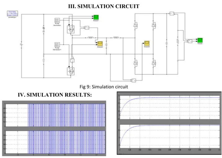
III. SIMULATION CIRCUIT
VI. REFERENCES:
[1] W. Wongsaichua, W. J. Lee, S. Oraintara, C. Kwan, and F. Zhang, “Integrated high-speed intelligent utility tie unit for disbursed/renewable generation facilities,” IEEE Trans. Ind. Appl., vol. 41, no. 2, pp. 507–513, Mar./Apr. 2005.
[2] Z. Liang, R. Guo, J. Li, and A. Q. Huang, “A high-efficiency PV module integrated DC/DC converter for PV energy harvest in FREEDM systems,”IEEE Trans. Power Electron., vol. 26, no. 3, pp. 897–909, Mar. 2011. [3] A. M. Rahimi and A. Emadi, “Discontinuous-conduction mode DC/DC converters feeding constant-power loads,” IEEE Trans. Ind. Electron., vol. 57, no. 4, pp. 1318–1329, Apr. 2010.
[4] R. Morrison and M. G. Egan, “A new power-factor-corrected single transformer UPS design,” IEEE Trans. Ind. Appl., vol. 36, no. 1, pp. 171– 179, Jan./Feb. 2000. [5] Y. M. Lai, S.-C. Tan, and Y. M. Tsang, “Wireless control of load current sharing information for parallel-connected DC/DC power converters,” IET Power Electron., vol. 2, no. 1, pp. 14–21, Jan. 2009.
[6] S. M. Lukic, J. Cao, R. C. Bansal, F. Rodriguez, and A. Emadi, “Energy storage systems for automotive applications,” IEEE Trans. Ind. Electron., vol. 55, no. 6, pp. 2258–2267, Jun. 2008.
[7] F. Liu, J. Yan, and X. Ruan, “Zero-voltage and zero-current-switching PWM combined three-level DC/DC converter,” IEEE Trans. Ind. Electron., vol. 57, no. 5, pp. 1644–1654, May 2010.
[8] Y. M. Chen, Y. C. Liu, and S. H. Lin, “Double-input PWM DC/DC converter for high-/low-voltage sources,” IEEE Trans. Ind. Electron., vol. 53, no. 5, pp. 1538– 1545, Oct. 2006.
[9] C. Liu, A. Johnson, and J. S. Lai, “DC/DC converter for low-voltage fuel cell applications,” IEEE Trans. Ind. Appl., vol. 41, no. 6, pp. 1691–1697, Nov./Dec. 2005. [10] R. M. Cuzner, D. J. Nowak, A. Bendre, G. Oriti, and A. L. Julian, “Mitigating circulating common-mode currents between parallel soft-switched drive systems,” IEEE Trans. Ind. Appl., vol. 43, no. 5, pp. 1284–1294, Sep./Oct. 2007.
[11] M. Ilic and D. Maksimovic, “Interleaved zero-current-transition buck converter,” IEEE Trans. Ind. Appl., vol. 43, no. 6, pp. 1619–1627, Nov./Dec. 2007. [12] M. L. da Silva Martins, J. L. Russi, and H. L. Hey, “Novel design methodology and comparative analysis for ZVT PWM converters with resonant auxiliary circuit,” IEEE Trans. Ind. Appl., vol. 42, no. 3, pp. 779– 796, May/Jun. 2006.
[13] Y. C. Chuang, Y. L. Ke, H. S. Chuang, and H. K. Chen, “Implementation and analysis of an improved series-loaded resonant DC-DC converter operating above resonance for battery chargers,” IEEE Trans. Ind. Appl., vol. 46, no. 3, pp. 1052–1059, May/Jun. 2009.
AUTHOR PROFILE:
1*CHIRANJEEVI GARAPATI is pursuing M.Tech in Nimra College of Engineering and Technology, Vijayawada, JNTU Kakinada. His specialization is Power Electronics. He graduated in Electrical and Electronics Engineering from PEC, JNTU Kakinada. His research interest includes Power Electronics and Applications.
2*SK GOUSE BASHA is currently working as a Assistant Professor in Electrical and Electronics Engineering Department, Nimra College of Engineering and Technology (NCET), Vijayawada. He obtained his M.Tech Degree & B.Tech degree in Electrical and Electronics Engineering from NCET, Vijayawada, JNTU Kakinada. His research interest includes Power Electronic Converters and applications.
3*RAVIKUMAR REDDY P is pursuing M.Tech in Nimra College of Engineering and Technology, Vijayawada, JNTU Kakinada. His specialization is Power & Industrial Drives. He graduated in Electrical and Electronics Engineering from Madina Engineering College, JNTU Anantapur in 2009. His research interest includes Power Electronics, Industrial Drives and Applications.