WP-01099-1.1 White Paper
Copyright © 2010 Altera Corporation. All rights reserved. Altera, The Programmable Solutions Company, the stylized Altera logo, and specific device designations are trademarks and/or service marks of Altera Corporation in the U.S. and other countries. All other words and logos identified as trademarks and/or service marks are the property of Altera Corporation or their respective owners. Altera products are protected under numerous U.S. and foreign patents and pending applications, maskwork rights, and copyrights. Altera warrants performance of its semiconductor products to current specifications in accordance with Altera's standard warranty, but reserves the right to make changes to any products and services at any time without notice. Altera assumes no responsibility or liability arising out of the application or use of any information, product, or service described herein except as expressly agreed to in writing by Altera. Altera customers are advised to obtain the latest version of device specifications before relying on any published information and before placing orders for products or services. 101 Innovation Drive
San Jose, CA 95134 www.altera.com
Implementing a Multirate Uncompressed
Video Interface for Broadcast
Applications
As high definition is established as the de facto standard for video broadcast around the world, new production equipment not only must cope with the 1080p video interface, but also must be able to handle the legacy of standard-definition and 1080i interfaces.
Introduction
The emergence of the high-definition (HD) 1080p video standard has presented some formidable design challenges for broadcast system engineers. While HD broadcasting now is established as the de facto standard for video broadcast around the world, new production equipment still must be able to handle the legacy of standard-definition (SD) and 1080i interfaces. This puts equipment manufacturers under pressure to build a cost-effective video interface solution that can handle multi-rate video. High-speed FPGA ICs, design tools, and off-the-shelf video IP cores help the designer create a wide variety of broadcast solutions, such as video switcher/routers, video servers, and video encoders, in time for market demand.
Video Background
Video interface standards have evolved a long way from the early days of NTSC and PAL composite analog video. The Society of Motion Picture and Television Engineers (SMPTE) has defined various video serial digital interface (SDI) standards from SD to HD. These standards are used for transmission of uncompressed digital video signals with embedded audio or control data within studio and broadcast facilities. They are designed for operation over short distances as they are inappropriate for long-distance transmission due to their high bitrates. Currently, SDI video is only available in professional video equipment such as switchers (the gateways that handle all the incoming video contents’ traffic from sources to destinations), servers (that store the video contents for later retrieval), and encoders (which compress the raw SDI video before distribution to consumers).
Both SD and HD SDI video use coaxial cable with a nominal impedance of 75. The specified signal amplitude at the source is 800 mV (±10 percent) peak to peak. Using the proper cable equalizer and driver can extend the maximum distance to 300 meters. HD bitrates have a shorter maximum run length, typically up to 200 meters. The uncompressed digital video signals are transmitted within the broadcast studio by encoding them in non-return-to-zero inverted (NRZI) format, and linear shift registers scramble the data to reduce the likelihood of long strings of zeroes or ones on the interface. The interface is self-synchronizing and self-clocking, with framing managed by detecting a special package bit pattern that is not legal anywhere else within the data payload.
Page 2 Video Background
Serial video transmission is now the industry standard, beginning with the original 270-Mbps SD video to the latest 2.97 Gbps or 3G-SDI for 1080p video resolution. These changes make it challenging for broadcast design engineers to achieve
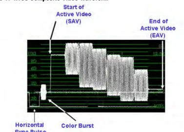
optimum performance at this high data rate with available silicon. In addition, video technology has evolved a long way since analog NTSC or PAL video signals. The analog video waveform has timing information on the horizontal blanking interval, reference timing, active picture, and color reference. Figure 1 shows a NTSC analog signal that contains all the timing information to be translated or mapped into the digital domain.
Figure 1. NTSC Composite Video Waveform
Component video, or YPbPr (Figure 2), quickly evolved from composite video. The original analog video was converted into “luma” and “chroma” components, allowing a method called chroma sub-sampling to reduce the amount video data for transport or storage. The digitized version of YPbPr is YCbCr, where Y is the luma component and Cb and Cr are the blue-difference and red-difference chroma
components. The digitized component video is multiplexed and serialized to become a SDI video stream.
Figure 2. Analog Component Video
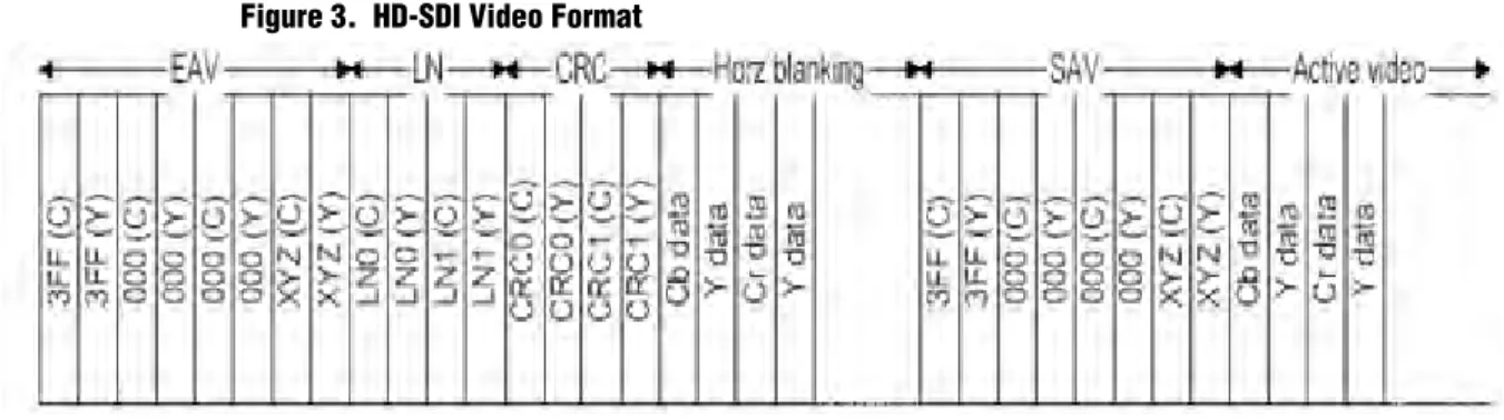
The SDI data video packets operate under the YCbCr domain in serial format
(Figure 3) for a HD-SDI video stream. The luma and chroma are interlaced with Cb as the first data bit. The SDI data rate is 270 Mbps for SD, 1.485 or (1.485/1.001) Gbps for 1080i HD, and 2.97 or (2.97/1.001) Gbps for 1080p 3G-SDI. The majority of broadcast equipment, such as studio switcher/routers, video servers, and encoders, must be upgraded to the triple-rate SDI mode to meet current and future requirements, especially for 1080p video resolution.
40-nm Technology in Broadcast Applications Page 3
Figure 3. HD-SDI Video Format
40-nm Technology in Broadcast Applications
Altera® Arria® II GX and Arria II GZ FPGAs are a cost-effective transceiver-based
FPGA family that provides a sweet spot for handling all SDI data-rate traffic in a low-channel-count environment. Arria II GX and Arria II GZ FPGAs offer high-speed serial connectivity with transceivers that deliver best-in-class signal integrity and jitter performance. The transceivers include both a physical coding sublayer (PCS) and a physical media attachment sublayer (PMA), deliver excellent jitter
performance, and minimize power, cost, and simultaneous switching noise (SSN) for broadcast applications.
Arria II GX and Arria II GZ transceivers are structured into full-duplex 4-channel transceiver blocks. Each block or quad has four input and four output channels. The smallest device has one block of transceivers, while the largest device has four blocks to handle up to sixteen SDI channels. The native transceiver’s data rate is between 600 Mbps to 6.375 Gbps, so an oversampling scheme is used for SD-SDI, which is 270 Mbps. Within each transceiver block, there are two clock multiplier units that provide the serial and parallel clocks to the transceiver channels.
Receive Path
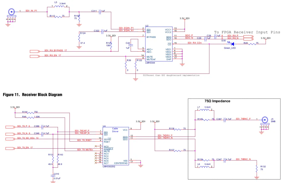
The receive data path contains a PMA block and a PCS block. The PMA’s input buffer connects to the external SDI cable equalizer. The serial clock is recovered by the clock data recovery (CDR) unit, which then is followed by the deserializer to produce a 10-/20-/40-bits parallel video data packet (depending on the video resolution). The PCS block contains the word aligner and FIFO buffers. The receive buffer supports a wide variety of standard SDI cable equalizer interface voltages. Table 1 shows the electrical specification for the input interfaces, and Figure 10 (see Appendix) shows the actual circuit interface to an external cable equalizer. The SDI input impedance to the equalizer is 75 and AC coupled. Proper layout according to the manufacturer’s guidelines is important for the best jitter performance.
Table 1. Input Electrical Features
I/O Standard Differential On-Chip Termination With Calibration () Common Mode Voltage (V) Coupling
1.4V PCML 85, 100, 120, 150 0.82 AC, DC
1.5V PCML 85, 100, 120, 150 0.82 AC, DC
2.5V PCML 85, 100, 120, 150 0.82 AC
LVPECL 85, 100, 120, 150 0.82 AC
Page 4 Transmit Path
Each receiver has an independent CDR unit to recover the embedded incoming high-speed serial clock and to produce a slow-high-speed parallel clock. Both recovered clocks are used to time the receiver PMA and PCS blocks. The reference clock input for the CDR unit can be derived either from a fixed clock source or from a voltage-controlled crystal oscillator (VCXO)-generated clock. A VCXO-generated clock is recommended if the transmitter needs to use the recovered clock as a transmit reference clock. In addition to the hard-wired receiver functions, Altera’s SDI MegaCore® function
provides a user-friendly implementation of the SDI receiver design. Arria II GX and Arria II GZ FPGAs can be selected among other transceiver families. The SDI MegaCore function includes:
■ NRZI decoding and descrambling for SDI data
■ Word alignment: End of active video (EAV) and start of active video (SAV)
sequences are used to determine the correct word alignment
■ Video timing flags extraction: The timing reference signal (TRS) module extracts F, V, and H video timing
■ RP168 switching: Allows video switching with a defined order using known
packets
■ HD line number (LN) extraction and cyclic redundancy check (CRC)
The SDI receive section is arranged into a protocol block and a receiver block. The protocol block is implemented by the Arria II GX or Arria II GZ logic core, while the receiver block uses the hard-wired receiver function, shown in Figure 4.
Figure 4. SDI Receiver MegaCore Block Diagram
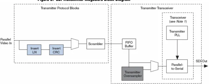
Transmit Path
The transmit path includes a transmit phase-compensation FIFO buffer, a serializer, and a transmitter output buffer. The transmit phase-compensation FIFO buffer joins the transmitter channel PCS and the FPGA fabric interface. It compensates for the phase difference between the low-speed parallel clock and the FPGA fabric interface clock. The output buffer connects to an external cable driver that drives a 75 video cable to 200 meters. As illustrated in Figure 11 (see Appendix), the actual external driver circuit has all AC-coupled signals, similar to the receiver interface circuit.
Performance Measurement Page 5
The SDI MegaCore function also provides a MegaWizard™ Plug-In to:
■ Configure the transmit interface functions
■ Perform HD LN insertion
■ Perform HD CRC generation and insertion
■ Perform scrambling and NRZI coding
The SDI transmitter (Figure 5) accepts 20-bit parallel video data for HD and 10-bit parallel data for SD.
Figure 5. SDI Transmitter MegaCore Block Diagram
f For further information on all of the functional blocks, refer to the SDI MegaCore
Function User Guide.
Arria II GX and Arria II GZ FPGAs offer broadcast engineers a powerful hardware device, design tools, and soft content to jump-start the design cycle. The transceivers accommodate all SDI data rates from SD to 3G with a single reference clock and without reconfiguration. The SDI MegaCore function, Quartus® design tools, and a
reference design allow a systematic approach to creating a triple-rate SDI broadcast system.
Performance Measurement
The challenges in transmitting a 1080p 3G-SDI video are amplified in the broadcast studio when using 75 coaxial cables originally designed for 270 Mbps. A copper coaxial cable has a fixed amount of bandwidth to carry high-speed data, before attenuation and noise (in the form of jitter) are added to the signal. Signal attenuation along a long cable also effects frequency domain. Therefore, every SDI receive input has a cable equalizer to increase the amplitude and “open up the eye” so the CDR unit inside the FPGA can recover the clock and data. When the equalizer has to increase the gain to compensate for lost amplitude, this can introduce noise and therefore produce jitter into the FPGA receiver.
Page 6 Performance Measurement
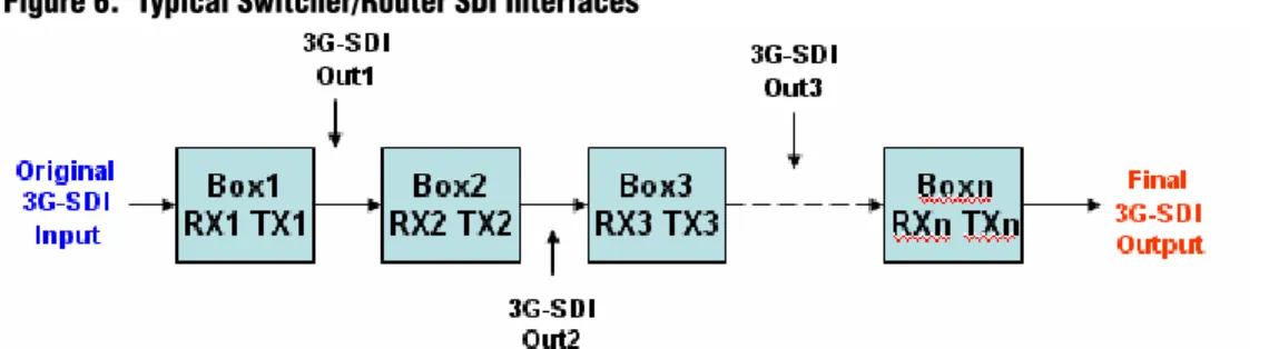
Some reclocker circuits can regenerate a SDI signal when connecting a few pieces of equipment, but can add unwanted time delay to the video path when a large system such as a video switcher/router is used. Therefore, it is critical that a FPGA SDI transmitter generates a very clean and extremely low jitter SDI source so there is enough margin budget left at the receiving end. The receiver of the FPGA then must tolerate a huge amount of jitter and still able to recover the data and recreate a clean clock for the next stage of transmission. This process repeats as necessary for a large broadcast switcher/router, as shown in Figure 6.
Figure 6. Typical Switcher/Router SDI Interfaces
40-nm Arria II GX and Arria II GZ FPGAs simplify the challenges of designing for signal integrity by providing transceivers with best-in-class jitter characteristics well beyond the SMPTE jitter specification. Advanced features in these transceivers simplify PCB design and compensate for inevitable board losses through multi-tap pre-emphasis, programmable VOD and on-chip termination. The phase-locked loops (PLLs) within the Arria II GX and Arria II GZ transceiver block provide the needed frequency and timing stability to create a serial data stream from the parallel domain inside the FPGA.
The jitter amplitude is important for overall SDI transmission, but is useless without knowing the frequencies of the jitter noise. Therefore, a broadcast engineer must measure both the amplitude and frequency of the jitter’s characteristics to know the performance of the equipment. SDI-specific test equipment is used to measure the overall jitter of the transceiver.
Two types of jitter measurements, timing jitter and alignment jitter, are defined by SMPTE. Timing jitter is short-term variations of significant instants of a digital signal from their ideal positions in time. Excessive timing jitter causes pixel dropouts or synchronizing errors in the receiver. Alignment jitter is deviation in time of significant instants of the SDI signal relative to a hypothetical clock recovered from the SDI signal itself. Excessive alignment jitter introduces decoding errors of the received SDI signal, so is related to how much tolerance a receiver’s clock recovery can handle before errors occur.
SMPTE defined the jitter specification to provide a reference for broadcast equipment manufacturers. As Table 2 shows, the 1080p 3G-SDI interface’s specification is the most drastic since the data rate is so high. The amount of jitter depends on the frequency of the signals as expressed in unit intervals (UIs), which are the inverse of the frequency.
Table 2. SMPTE Jitter Specifications
Specification Frequency 1 UI
SD-SDI 270 Mbps 3.7 ns
HD-SDI 1.4835 Gbps 0.67 ns
Reference Design Page 7
For the SMPTE standards, timing jitter has a lower frequency limit of 10 Hz. SMPTE specifies the timing jitter for the 3G-SDI to be 2 UIs. Any jitter frequency components below 10 Hz are called “wander,” which is not addressed in the SMPTE standards. Most equipment’s SDI receivers can track this slow moving jitter. The frequency bandpass starts from 10 Hz for measuring timing jitter (Figure 7) and from 100 KHz for alignment jitter (Figure 8).
Figure 7. Timing Jitter Bandwidth
Figure 8. Alignment Jitter Bandwidth
Reference Design
A triple-rate 1080p SDI loop-through reference design demonstrates the autodetection capability of the Arria II GX or Arria II GZ FPGA, so the receiver can detect whether the incoming video stream is SD, HD, or 3G for 1080p. The Arria II GX or Arria II GZ FPGA’s dynamic partially reconfigurable I/Os (DPRIOs) are used to perform the data-rate detection and lock to the SDI rates. Once the CDR unit in the receiver block locks to the incoming data, the core decodes the serial bits for the parallel domain. The parallel data is re-encoded and re-routed back to serial format at the transmitter. For the triple-rate transmitter demonstration or jitter-generation test, the design outputs a 2.970-Gbps 1080p, 1.485-Gbps 1080i, or 270-Mbps data stream. It takes its input from the internal pattern generator, using 100 percent colorbar pattern, a 75 percent amplitude colorbar pattern, or an SDI pathological checkfield frame pattern. For the triple-rate duplex, the MegaCore function provides a full duplex 3-Gbps SDI, HD-SDI, and SD-SDI, and demonstrates receiver-to-transmitter loopback. A phase-frequency detector takes in the CDR clock and the transmitter reference clock and compares their phase and frequency. The phase-frequency detector then adjusts the external-transmitter reference-clock source, so the signals match in phase and frequency. The phase-frequency detector allows the designer to lock a low-jitter transmit reference clock to the recovered clock from the SDI input. The received data
Page 8 Conclusion
is decoded, buffered, and recoded, then transmitted. The decoded receiver data is connected to the transmitter input through a FIFO buffer. When the receiver is locked, the receiver data is written to the FIFO buffer. When the FIFO buffer is half-full, the transmitter starts reading, encoding, and transmitting the data. The VCXO provides a clean source of reference clock for the transceivers.
This reference design, illustrated in Figure 9, is part of Quartus II design software version 9.0. It can be used to measure system performance such as jitter tolerance and generation, and can be modified and recompiled from the restored SDI Quartus archive file.
Figure 9. Reference Design Example Block Diagram
f The reference design can be downloaded from Altera’s Broadcast Reference Designs
webpage.
Conclusion
Arria II GX and Arria II GZ FPGAs, along with the industry proven SDI MegaCore function, provide a cost-effective way to implement 1080p 3G-SDI video interface for the broadcast industry. The programmable fabric and multi-rate transceivers help designers implement their designs quickly. The superior jitter performance of Arria II GX and Arria II GZ FPGA’s transceivers allows equipment to interface with various broadcast products from SD to 3G-SDI.
Ap pe nd ix Page 9 July 2010 Alter a Corporatio n Implementing a Multira te U n compr essed Vi deo Int erface for Br oa dca st Applications
Appendix
Figure 10. SDI Cable Equalizer Interface
Figure 11. Receiver Block Diagram 1 2 3 4 5 R39 0 R124 37.4
To FPGA Receiver Input Pins SDI_IN_P1 SDI_EQIN_N1 SDI_EQIN_P1 SDI_RX_CDn VEE1 1 VEE2 4 SDI 2 SDI 3 AEC+ 5 AEC-6 BYPASS 7 MUTEref 8 VEE3 9 SDO 11 SDO 10 VEE4 12 MUTE 14 CD 15 VCC1 13 VCC2 16 DAP 17 U2 LMH0344 C322 1uF R108 75 D30 Green_LED C311 1uF R122 0 R113 75 C42 1uF R123 10K R45 75 3.3V_SDI 3.3V_SDI 3.3V_SDI SDI_RX_N 8 SDI_RX_P 8 SDO_N C28 1uF SDO_P C29 1uF SDI_RX_BYPASS 17 1 L5 3.9nH2
DIfferent than SDI daughtercard implementation
SDI_RX_EN 17 1L7 5.6nH2 SDI_TX_MUTEn SDI_TXBNC_P SDI_TXBNC_N SDI_TX_RSET R139 75 SDI 1 SDI 2 VEE 3 RSET 4 VCC 9 SD/HD 10 SDOSDO 1211 CENTERPAD 17 NC0 5 DISABLE 6 MUTE 7 NC3 8 NC4 13 NC5 14 NC6 15 NC7 16 Cable Driv er U4 LMH0302SQ C346 4.7uF C387 4.7uF 1 2 3 4 5 J5 SMB R46 1.00K C347 4.7uF R131 49.9 C386 4.7uF R138 75 SDI_TX_N 8 R137 75 C416 0.01uF R144 750 R143 49.9 R145 75 R132 75 3.3V_SDI 3.3V_SDI 3.3V_SDI 75Ω Impedance SDI_TXDRV_P 1L6 5.6nH2 SDI_TX_EN 17 SDI_TX_SD_HDn 10 SDI_TXCAP_P SDI_TXCAP_N SDI_TX_P 8 SDI_TXDRV_N
Page 10 Further Information
Further Information
■ Arria II GX FPGAs: Cost-Optimized, Lowest Power 6G Transceiver FPGAs:
www.altera.com/products/devices/arria-fpgas/arria-ii-gx/aiigx-index.jsp
■ SDI MegaCore Function User Guide:
www.altera.com/literature/ug/ug_sdi.pdf
■ Broadcast Reference Designs:
www.altera.com/support/refdesigns/sys-sol/broadcast/broad-index.jsp
Acknowledgements
■ Tam Do, Senior Technical Marketing Manager, Broadcast Business Unit, Altera
Corporation
Document Revision History
Table 3 shows the revision history for this document. Table 3. Document Revision History
Date Version Changes
July 2010 1.1 ■ Updated Further Information.
■ Minor text edits. March 2009 1.0 Initial release.