– Datasheet Describes Mode 0 Operation • Low-voltage and Standard-voltage Operation
– 2.7 (VCC= 2.7V to 5.5V) – 1.8 (VCC= 1.8V to 5.5V) • 20 MHz Clock Rate (5V) • 32-byte Page Mode • Block Write Protection
– Protect 1/4, 1/2, or Entire Array
• Write Protect (WP) Pin and Write Disable Instructions for Both Hardware and Software Data Protection
• Self-timed Write Cycle (5 ms max) • High Reliability
– Endurance: One Million Write Cycles – Data Retention: 100 Years
• Available in Automotive
• 8-lead JEDEC PDIP, 8-lead JEDEC SOIC, 8-lead TSSOP, 8-lead MAP, 8-lead Ultra Thin Mini-MAP (MLP 2x3) and 8-lead TSSOP Packages
• Die Sales: Wafer Form, Tape and Reel, and Bumped Wafers
Description
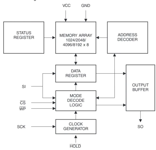
The AT25080A/160A/320A/640A provides 8192/16384/32768/65536 bits of serial electrically-erasable programmable read-only memory (EEPROM) organized as 1024/2048/4096/8192 words of 8 bits each. The device is optimized for use in many industrial and commercial applications where low-power and low-voltage operation are essential. The AT25080A/160A/320A/640A is available in space-saving 8-lead PDIP, lead JEDEC SOIC, lead MAP, lead Ultra Thin Mini-MAP (MLP 2x3), 8-lead TSSOP and 8-Lead Ultra Leadframe Land Grid Array (ULLGA) packages. The AT25080A/160A/320A/640A is enabled through the Chip Select pin (CS) and accessed via a three-wire interface consisting of Serial Data Input (SI), Serial Data Output (SO), and Serial Clock (SCK). All programming cycles are completely self-timed, and no separate erase cycle is required before write.
SPI Serial
EEPROMs
8K (1024 x 8)
16K (2048 x 8)
32K (4096 x 8)
64K (8192 x 8)
AT25080A
AT25160A
AT25320A
AT25640A
Not
Recommended
for New Design
Block write protection is enabled by programming the status register with one of four blocks of write protection. Separate program enable and program disable instructions are provided for additional data protection. Hardware data protection is provided via the WP pin to protect against inadvertent write attempts to the status register. The HOLD pin may be used to suspend any serial communication without resetting the serial sequence.
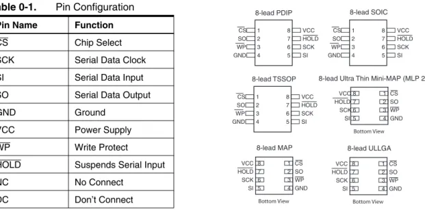
Table 0-1. Pin Configuration Pin Name Function
CS Chip Select
SCK Serial Data Clock
SI Serial Data Input
SO Serial Data Output
GND Ground
VCC Power Supply
WP Write Protect
HOLD Suspends Serial Input
NC No Connect
DC Don’t Connect
1.
Absolute Maximum Ratings*
Operating Temperature ... –55C to +125C *NOTICE: Stresses beyond those listed under “Absolute Maximum Ratings” may cause permanent dam-age to the device. This is a stress rating only and functional operation of the device at these or any other conditions beyond those indicated in the operational sections of this specification is not implied. Exposure to absolute maximum rating conditions for extended periods may affect device reliability.
Storage Temperature... –65C to +150C Voltage on Any Pin
with Respect to Ground ...–1.0V to +7.0V Maximum Operating Voltage ... 6.25V DC Output Current... 5.0 mA 1 2 3 4 8 7 6 5 CS SO WP GND VCC HOLD SCK SI 8-lead PDIP 1 2 3 4 8 7 6 5 CS SO WP GND VCC HOLD SCK SI 8-lead SOIC 1 2 3 4 8 7 6 5 CS SO WP GND VCC HOLD SCK SI 8-lead TSSOP 1 2 3 4 8 7 6 5 VCC HOLD SCK SI CS SO WP GND
8-lead Ultra Thin Mini-MAP (MLP 2x
Bottom View 1 2 3 4 8 7 6 5 VCC HOLD SCK SI CS SO WP GND 8-lead ULLGA Bottom View 1 2 3 4 8 7 6 5 VCC HOLD SCK SI CS SO WP GND 8-lead MAP Bottom View
Figure 1-1. Block Diagram
Note: 1. This parameter is characterized and is not 100% tested. Table 1-1. Pin Capacitance(1)
Applicable over recommended operating range from TA= 25C, f = 1.0 MHz, VCC= +5.0V (unless otherwise noted)
Symbol Test Conditions Max Units Conditions
COUT Output Capacitance (SO) 8 pF VOUT= 0V
Notes: 1. VILmin and VIHmax are reference only and are not tested. 2. Worst case measured at 85C
Table 1-2. DC Characteristics
Applicable over recommended operating range from: TAI=–40C to +85C, VCC= +1.8V to +5.5V (unless otherwise noted)
Symbol Parameter Test Condition Min Typ Max Units
VCC1 Supply Voltage 1.8 5.5 V
VCC2 Supply Voltage 2.7 5.5 V
VCC3 Supply Voltage 4.5 5.5 V
ICC1 Supply Current VCC= 5.0V at 20 MHz, SO = Open, Read 7.5 10.0 mA
ICC2 Supply Current VCC= 5.0V at 20 MHz, SO = Open, Read,
Write 4.0 10.0 mA
ICC3 Supply Current VCC= 5.0V at 5 MHz, SO = Open,
Read, Write 4.0 6.0 mA
ISB1 Standby Current VCC= 1.8V, CS = VCC < 0.1 6.0(2) µA
ISB2 Standby Current VCC= 2.7V, CS = VCC 0.3 7.0(2) µA
ISB3 Standby Current VCC= 5.0V, CS = VCC 2.0 10.0(2) µA
IIL Input Leakage VIN= 0V to VCC –3.0 3.0 µA
IOL Output Leakage VIN= 0V to VCC, TAC= 0°C to 70°C –3.0 3.0 µA
VIL(1) Input Low-voltage –0.6 VCCx 0.3 V
VIH(1) Input High-voltage VCCx 0.7 VCC+ 0.5 V
VOL1 Output Low-voltage
4.5VVCC5.5V
IOL= 3.0 mA 0.4 V
VOH1 Output High-voltage IOH=1.6 mA VCC- 0.8 V
VOL2 Output Low-voltage
1.8VVCC3.6V
IOL= 0.15 mA 0.2 V
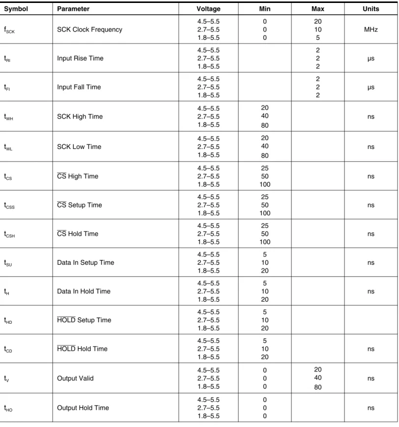
Table 1-3. AC Characteristics
Applicable over recommended operating range from TAI=–40C to +85C, VCC= As Specified, CL = 1 TTL Gate and 30 pF (unless otherwise noted)
Symbol Parameter Voltage Min Max Units
fSCK SCK Clock Frequency 4.5–5.5 2.7–5.5 1.8–5.5 0 0 0 20 10 5 MHz
tRI Input Rise Time
4.5–5.5 2.7–5.5 1.8–5.5 2 2 2 µs
tFI Input Fall Time
4.5–5.5 2.7–5.5 1.8–5.5 2 2 2 µs tWH SCK High Time 4.5–5.5 2.7–5.5 1.8–5.5 20 40 80 ns tWL SCK Low Time 4.5–5.5 2.7–5.5 1.8–5.5 20 40 80 ns tCS CS High Time 4.5–5.5 2.7–5.5 1.8–5.5 25 50 100 ns tCSS CS Setup Time 4.5–5.5 2.7–5.5 1.8–5.5 25 50 100 ns tCSH CS Hold Time 4.5–5.5 2.7–5.5 1.8–5.5 25 50 100 ns
tSU Data In Setup Time
4.5–5.5 2.7–5.5 1.8–5.5 5 10 20 ns
tH Data In Hold Time
4.5–5.5 2.7–5.5 1.8–5.5 5 10 20 ns
tHD HOLD Setup Time
4.5–5.5 2.7–5.5 1.8–5.5 5 10 20
tCD HOLD Hold Time
4.5–5.5 2.7–5.5 1.8–5.5 5 10 20 ns tV Output Valid 4.5–5.5 2.7–5.5 1.8–5.5 0 0 0 20 40 80 ns
tHO Output Hold Time
4.5–5.5 2.7–5.5 1.8–5.5 0 0 0 ns
Note: 1. This parameter is characterized and is not 100% tested.
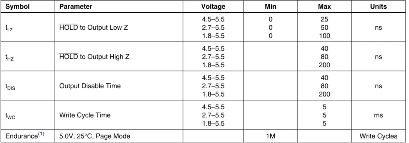
tLZ HOLD to Output Low Z
4.5–5.5 2.7–5.5 1.8–5.5 0 0 0 25 50 100 ns
tHZ HOLD to Output High Z
4.5–5.5 2.7–5.5 1.8–5.5 40 80 200 ns
tDIS Output Disable Time
4.5–5.5 2.7–5.5 1.8–5.5 40 80 200 ns
tWC Write Cycle Time
4.5–5.5 2.7–5.5 1.8–5.5 5 5 5 ms
Endurance(1) 5.0V, 25°C, Page Mode 1M Write Cycles
Table 1-3. AC Characteristics (Continued)
Applicable over recommended operating range from TAI=–40C to +85C, VCC= As Specified, CL = 1 TTL Gate and 30 pF (unless otherwise noted)
2.
Serial Interface Description
MASTER:The device that generates the serial clock.
SLAVE:Because the Serial Clock pin (SCK) is always an input, the AT25080A/160A/320A/640A always operates as a slave.
TRANSMITTER/RECEIVER: The AT25080A/160A/320A/640A has separate pins designated for data transmission (SO) and reception (SI).
MSB:The Most Significant Bit (MSB) is the first bit transmitted and received.
SERIAL OP-CODE:After the device is selected with CS going low, the first byte will be received. This byte contains the op-code that defines the operations to be performed.
INVALID OP-CODE: If an invalid op-code is received, no data will be shifted into the AT25080A/160A/320A/640A, and the serial output pin (SO) will remain in a high impedance state until the falling edge of CS is detected again. This will reinitialize the serial communication. CHIP SELECT:The AT25080A/160A/320A/640A is selected when the CS pin is low. When the device is not selected, data will not be accepted via the SI pin, and the serial output pin (SO) will remain in a high impedance state.
H O L D : T h e H O L D p i n i s u s e d i n c o n j u n c t i o n w i t h t h e C S p i n t o s e l e c t t h e AT25080A/160A/320A/640A. When the device is selected and a serial sequence is underway, HOLD can be used to pause the serial communication with the master device without resetting the serial sequence. To pause, the HOLD pin must be brought low while the SCK pin is low. To resume serial communication, the HOLD pin is brought high while the SCK pin is low (SCK may still toggle during HOLD). Inputs to the SI pin will be ignored while the SO pin is in the high impedance state.
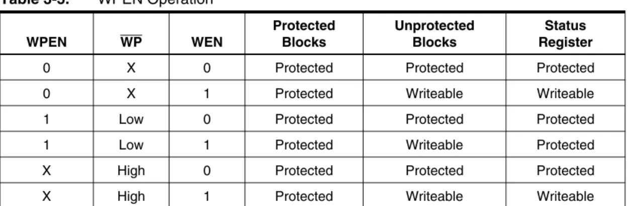
WRITE PROTECT:The write protect pin (WP) will allow normal read/write operations when held high. When the WP pin is brought low and WPEN bit is “1”, all write operations to the status reg-ister are inhibited. WP going low while CS is still low will interrupt a write to the status regreg-ister. If the internal write cycle has already been initiated, WP going low will have no effect on any write operation to the status register. The WP pin function is blocked when the WPEN bit in the status register is “0”. This will allow the user to install the AT25080A/160A/320A/640A in a system with the WP pin tied to ground and still be able to write to the status register. All WP pin functions are enabled when the WPEN bit is set to “1”.
Figure 2-1. SPI Serial Interface
3.
Functional Description
The AT25080A/160A/320A/640A is designed to interface directly with the synchronous serial peripheral interface (SPI) of the 6805 and 68HC11 series of microcontrollers.
The AT25080A/160A/320A/640A utilizes an 8-bit instruction register. The list of instructions and their operation codes are contained inTable 3-1. All instructions, addresses, and data are trans-ferred with the MSB first and start with a high-to-low CS transition.
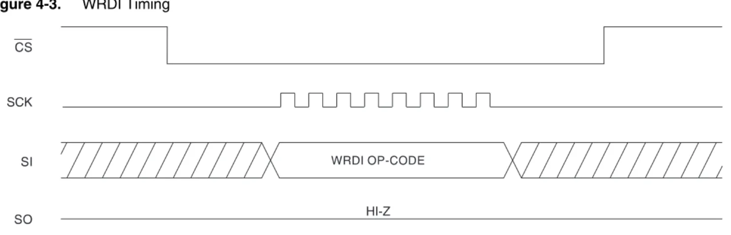
WRITE ENABLE (WREN): The device will power up in the write disable state when VCCis applied. All programming instructions must therefore be preceded by a Write Enable instruction. WRITE DISABLE (WRDI):To protect the device against inadvertent writes, the Write Disable instruction disables all programming modes. The WRDI instruction is independent of the status of the WP pin.
READ STATUS REGISTER (RDSR):The Read Status Register instruction provides access to the status register. The READY/BUSY and Write Enable status of the device can be determined by the RDSR instruction. Similarly, the Block Write Protection Bits indicate the extent of protec-tion employed. These bits are set by using the WRSR instrucprotec-tion.
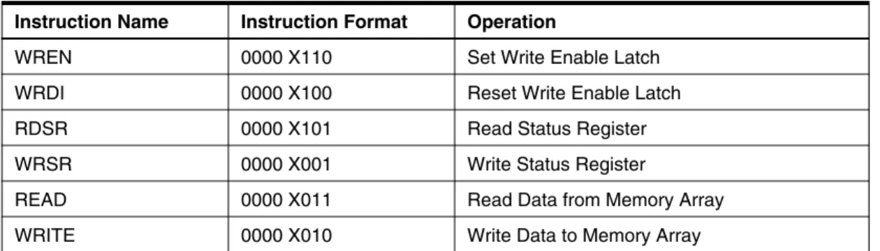
Table 3-1. Instruction Set for the AT25080A/160A/320A/640A Instruction Name Instruction Format Operation
WREN 0000 X110 Set Write Enable Latch
WRDI 0000 X100 Reset Write Enable Latch
RDSR 0000 X101 Read Status Register
WRSR 0000 X001 Write Status Register
READ 0000 X011 Read Data from Memory Array
WRITE 0000 X010 Write Data to Memory Array
Table 3-2. Status Register Format
Bit 7 Bit 6 Bit 5 Bit 4 Bit 3 Bit 2 Bit 1 Bit 0
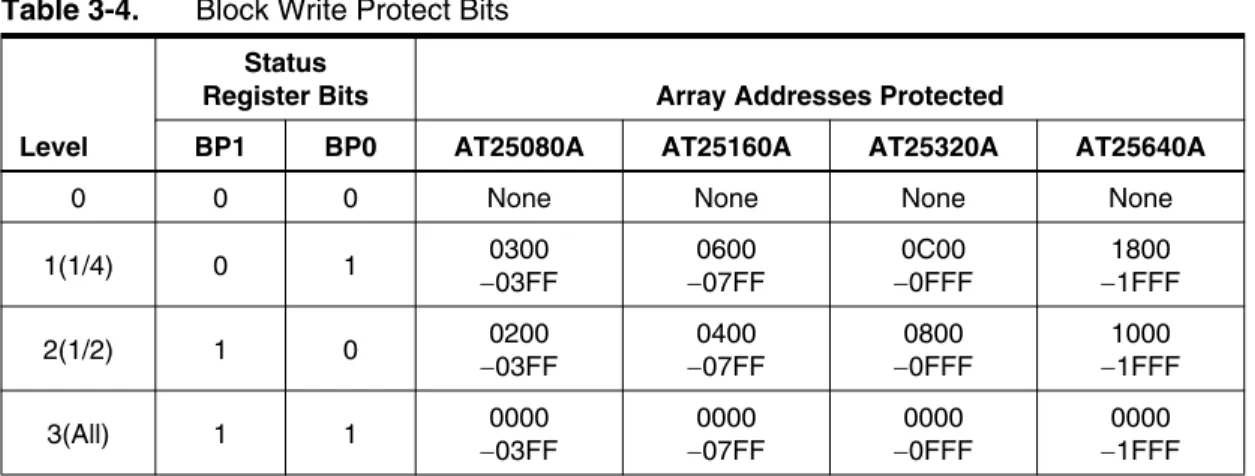
WRITE STATUS REGISTER (WRSR):The WRSR instruction allows the user to select one of four levels of protection. The AT25080A/160A/320A/640A is divided into four array segments. One-quarter, one-half, or all of the memory segments can be protected. Any of the data within any selected segment will therefore be read only. The block write protection levels and corre-sponding status register control bits are shown inTable 3-4.
The three bits BP0, BP1, and WPEN are nonvolatile cells that have the same properties and functions as the regular memory cells (e.g., WREN, tWC, RDSR).
The WRSR instruction also allows the user to enable or disable the write protect (WP) pin through the use of the Write Protect Enable (WPEN) bit. Hardware write protection is enabled when the WP pin is low and the WPEN bit is “1”. Hardware write protection is disabled when either the WP pin is high or the WPEN bit is “0”. When the device is hardware write protected, writes to the status register, including the block protect bits and the WPEN bit, and the block-pro-tected sections in the memory array are disabled. Writes are only allowed to sections of the memory that are not block-protected.
NOTE:When the WPEN bit is hardware write protected, it cannot be changed back to “0” as long as the WP pin is held low.
Table 3-3. Read Status Register Bit Definition
Bit Definition
Bit 0 (RDY) Bit 0 = “0” (RDY) indicates the device is READY. Bit 0 = “1” indicates the write cycle is in progress.
Bit 1 (WEN) Bit 1= “0” indicates the device is not WRITE ENABLED. Bit 1 = “1” indicates the device is write enabled.
Bit 2 (BP0) SeeTable 3-4 on page 10. Bit 3 (BP1) SeeTable 3-4 on page 10.
Bits 4–6 are “0”s when device is not in an internal write cycle. Bit 7 (WPEN) SeeTable 3-5 on page 11.
Bits 0–7 are “1”s during an internal write cycle.
Table 3-4. Block Write Protect Bits
Level
Status
Register Bits Array Addresses Protected
BP1 BP0 AT25080A AT25160A AT25320A AT25640A
0 0 0 None None None None
1(1/4) 0 1 0300 03FF 0600 07FF 0C00 0FFF 1800 1FFF 2(1/2) 1 0 0200 03FF 0400 07FF 0800 0FFF 1000 1FFF 3(All) 1 1 0000 03FF 0000 07FF 0000 0FFF 0000 1FFF
READ SEQUENCE (READ):Reading the AT25080A/160A/320A/640A via the Serial Output (SO) pin requires the following sequence. After the CS line is pulled low to select a device, the read op-code is transmitted via the SI line followed by the byte address to be read (A15–A0, see
Table 3-6). Upon completion, any data on the SI line will be ignored. The data (D7–D0) at the specified address is then shifted out onto the SO line. If only one byte is to be read, the CS line should be driven high after the data comes out. The read sequence can be continued since the byte address is automatically incremented and data will continue to be shifted out. When the highest address is reached, the address counter will roll over to the lowest address allowing the entire memory to be read in one continuous read cycle.
WRITE SEQUENCE (WRITE):In order to program the AT25080A/160A/320A/640A, two sepa-rate instructions must be executed. First, the devicemust be write enabledvia the WREN instruction. Then a write (WRITE) instruction may be executed. Also, the address of the memory location(s) to be programmed must be outside the protected address field location selected by the block write protection level. During an internal write cycle, all commands will be ignored except the RDSR instruction.
A write instruction requires the following sequence. After the CS line is pulled low to select the device, the WRITE op-code is transmitted via the SI line followed by the byte address (A15–A0) and the data (D7–D0) to be programmed (seeTable 3-6). Programming will start after the CS pin is brought high. The low-to-high transition of the CS pin must occur during the SCK low-time immediately after clocking in the D0 (LSB) data bit.
The READY/BUSY status of the device can be determined by initiating a read status register (RDSR) instruction. If Bit 0 = “1”, the write cycle is still in progress. If Bit 0 = “0”, the write cycle has ended. Only the RDSR instruction is enabled during the write programming cycle.
The AT25080A/160A/320A/640A is capable of a 32-byte page write operation. After each byte of data is received, the five low-order address bits are internally incremented by one; the high-order bits of the address will remain constant. If more than 32 bytes of data are transmitted, the address counter will roll over and the previously written data will be overwritten. The AT25080A/160A/320A/640A is automatically returned to the write disable state at the comple-tion of a write cycle.
NOTE:If the device is not write-enabled (WREN), the device will ignore the write instruction and will return to the standby state, when CS is brought high. A new CS falling edge is required to reinitiate the serial communication.
Table 3-5. WPEN Operation
WPEN WP WEN Protected Blocks Unprotected Blocks Status Register
0 X 0 Protected Protected Protected
0 X 1 Protected Writeable Writeable
1 Low 0 Protected Protected Protected
1 Low 1 Protected Writeable Protected
X High 0 Protected Protected Protected
4.
Timing Diagrams
Figure 4-1. Synchronous Data Timing (for Mode 0)
Figure 4-2. WREN Timing
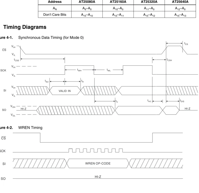
Table 3-6. Address Key
Address AT25080A AT25160A AT25320A AT25640A
AN A9–A0 A10–A0 A11–A0 A12–A0
Don’t Care Bits A15–A10 A15–A11 A15–A12 A15–A13
SO VOH VOL HI-Z HI-Z tV VALID IN SI VIH VIL tH tSU tDIS SCK VIH VIL tWH tCSH CS VIH VIL tCSS tCS tWL tHO
Figure 4-3. WRDI Timing Figure 4-4. RDSR Timing Figure 4-5. WRSR Timing CS SCK 0 1 2 3 4 5 6 7 8 9 10 11 12 13 14 SI INSTRUCTION SO 7 6 5 4 3 2 1 0 DATA OUT MSB HIGH IMPEDANCE 15 HIGH IMPEDANCE INSTRUCTION DATA IN 0 0 1 1 2 2 3 3 4 4 5 5 6 6 7 7 8 9 10 11 12 13 14 15 CS SCK SI SO
Figure 4-6. READ Timing
Figure 4-7. WRITE Timing
Figure 4-8. HOLD Timing CS SCK SI SO 0 0 0 1 1 1 2 2 2 3 3 3 ... 4 4 5 5 6 6 7 7 8 9 10 15 14 13 11 20 21 22 23 24 25 26 27 28 29 30 HIGH IMPEDANCE INSTRUCTION BYTE ADDRESS MSB DATA OUT 31 0 0 0 1 1 1 2 2 2 3 3 3 ... 4 4 5 5 6 6 7 7 8 9 10 15 14 13 11 20 21 22 23 24 25 26 27 28 29 30 31 HIGH IMPEDANCE CS SCK SI SO INSTRUCTION
BYTE ADDRESS DATA IN
SO SCK HOLD tCD tHD tHZ tLZ tCD tHD CS
Notes: 1. For 2.7V devices used in the 4.5 to 5.5V range, please refer to performance values in the AC and DC Characteristics tables. 2. “U” designates Green package + RoHS compliant.
3. “H” designates Green package + RoHS compliant, with NiPdAu Lead Finish.
4. Available in waffle pack and wafer form; order as SL788 for inkless wafer form. Bumped die available upon request. Please contact Serial EEPROM Marketing.
5.
AT25080A Ordering Information
(1)Ordering Code Package Operation Range
AT25080A-10PU-2.7(2) AT25080A-10PU-1.8(2) AT25080AN-10SU-2.7(2) AT25080AN-10SU-1.8(2) AT25080A-10TU-2.7(2) AT25080A-10TU-1.8(2)
AT25080AY1-10YU-1.8(2) (Not recommended for new design) AT25080AY6-10YH-1.8(3) 8P3 8P3 8S1 8S1 8A2 8A2 8Y1 8Y6 Lead-free/Halogen-free/ Industrial Temperature (40 to 85C)
AT25080A-W1.8-11(4) Die Sale Industrial Temperature
(40 to 85C)
Package Type 8P3 8-lead, 0.300" Wide, Plastic Dual Inline Package (PDIP)
8S1 8-lead, 0.150" Wide, Plastic Gull Wing Small Outline (JEDEC SOIC) 8A2 8-lead, 4.4 mm Body, Plastic Thin Shrink Small Outline Package (TSSOP)
8Y1 8-lead, 4.90 mm x 3.00 mm Body, Dual Footprint, Non-leaded, Miniature Array Package (MAP)
8Y6
8-lead, 2.00 mm x 3.00 mm Body, 0.50 mm Pitch, Ultra Thin Mini-MAP, Dual No Lead Package (DFN), (MLP 2x3mm)
Options
2.7 Low Voltage (2.7 to 5.5V) 1.8 Low Voltage (1.8 to 5.5V)
Notes: 1. For 2.7V devices used in the 4.5 to 5.5V range, please refer to performance values in the AC and DC Characteristics tables. 2. “U” designates Green package + RoHS compliant.
3. “H” designates Green package + RoHS compliant, with NiPdAu Lead Finish.
4. Available in waffle pack and wafer form; order as SL788 for inkless wafer form. Bumped die available upon request. Please contact Serial EEPROM Marketing.
6.
AT25160A Ordering Information
(1)Ordering Code Package Operation Range
AT25160A-10PU-2.7(2) AT25160A-10PU-1.8(2) AT25160AN-10SU-2.7(2) AT25160AN-10SU-1.8(2) AT25160A-10TU-2.7(2) AT25160A-10TU-1.8(2)
AT25160AY1-10YU-1.8(2) (Not recommended for new design) AT25160AY6-10YH-1.8(3) AT25160AD3-10DH-1.8 8P3 8P3 8S1 8S1 8A2 8A2 8Y1 8Y6 8D3 Lead-free/Halogen-free/ Industrial Temperature (40 to 85C)
AT25160A-W1.8-11(4) Die Sale Industrial Temperature
(40 to 85C)
Package Type 8P3 8-lead, 0.300" Wide, Plastic Dual Inline Package (PDIP)
8S1 8-lead, 0.150" Wide, Plastic Gull Wing Small Outline (JEDEC SOIC) 8A2 8-lead, 4.4 mm Body, Plastic Thin Shrink Small Outline Package (TSSOP)
8Y1 8-lead, 4.90 mm x 3.00 mm Body, Dual Footprint, Non-leaded, Miniature Array Package (MAP)
8Y6
8-lead, 2.00 mm x 3.00 mm Body, 0.50 mm Pitch, Ultra Thin Mini-MAP, Dual No Lead Package (DFN), (MLP 2x3mm)
8D3 8-lead, 1.80 mm x 2.20 mm Body, Ultra Lead Frame Land Grid Array (ULLGA) D3 Options
Notes: 1. For 2.7V devices used in the 4.5 to 5.5V range, please refer to performance values in the AC and DC Characteristics tables. 2. “U” designates Green package + RoHS compliant.
3. “H” designates Green package + RoHS compliant, with NiPdAu Lead Finish.
4. Available in waffle pack and wafer form; order as SL788 for inkless wafer form. Bumped die available upon request. Please contact Serial EEPROM Marketing.
7.
AT25320A Ordering Information
(1)Ordering Code Package Operation Range
AT25320A-10PU-2.7(2) AT25320A-10PU-1.8(2) AT25320AN-10SU-2.7(2) AT25320AN-10SU-1.8(2) AT25320A-10TU-2.7(2) AT25320A-10TU-1.8(2)
AT25320AY1-10YU-1.8(2) (Not recommended for new design) AT25320AY6-10YH-1.8(3) 8P3 8P3 8S1 8S1 8A2 8A2 8Y1 8Y6 Lead-free/Halogen-free/ Industrial Temperature (40 to 85C)
AT25320A-W1.8-11(4) Die Sale Industrial Temperature
(40 to 85C)
Package Type 8P3 8-lead, 0.300" Wide, Plastic Dual Inline Package (PDIP)
8S1 8-lead, 0.150" Wide, Plastic Gull Wing Small Outline (JEDEC SOIC) 8A2 8-lead, 4.4 mm Body, Plastic Thin Shrink Small Outline Package (TSSOP)
8Y1 8-lead, 4.90 mm x 3.00 mm Body, Dual Footprint, Non-leaded, Miniature Array Package (MAP)
8Y6
8-lead, 2.00 mm x 3.00 mm Body, 0.50 mm Pitch, Ultra Thin Mini-MAP, Dual No Lead Package (DFN), (MLP 2x3mm)
Options
Notes: 1. For 2.7V devices used in the 4.5 to 5.5V range, please refer to performance values in the AC and DC Characteristics tables. 2. “U” designates Green package + RoHS compliant.
3. “H” designates Green package + RoHS compliant, with NiPdAu Lead Finish.
4. Available in waffle pack and wafer form; order as SL788 for inkless wafer form. Bumped die available upon request. Please contact Serial EEPROM Marketing.
8.
AT25640A Ordering Information
(1)Ordering Code Package Operation Range
AT25640A-10PU-2.7(2) AT25640A-10PU-1.8(2) AT25640AN-10SU-2.7(2) AT25640AN-10SU-1.8(2) AT25640A-10TU-2.7(2) AT25640A-10TU-1.8(2)
AT25640AY1-10YU-1.8(2)(Not recommended for new design) AT25640AY6-10YH-1.8(3) 8P3 8P3 8S1 8S1 8A2 8A2 8Y1 8Y6 Lead-free/Halogen-free/ Industrial Temperature (40 to 85C)
AT25640A-W1.8-11(3) Die Sale Industrial Temperature
(40 to 85C)
Package Type 8P3 8-lead, 0.300" Wide, Plastic Dual Inline Package (PDIP)
8S1 8-lead, 0.150" Wide, Plastic Gull Wing Small Outline (JEDEC SOIC) 8A2 8-lead, 4.4 mm Body, Plastic Thin Shrink Small Outline Package (TSSOP)
8Y1 8-lead, 4.90 mm x 3.00 mm Body, Dual Footprint, Non-leaded, Miniature Array Package (MAP)
8Y6 8-lead, 2.00 mm x 3.00 mm Body, 0.50 mm Pitch, Ultra Thin Mini-MAP, Dual No Lead Package (DFN), (MLP 2x3 mm) Options
9.
Packaging Information
8P3 – PDIP
2325 Orchard Parkway San Jose, CA 95131
TITLE DRAWING NO.
R
REV. 8P3, 8-lead, 0.300" Wide Body, Plastic Dual
In-line Package (PDIP)
01/09/02
8P3 B
Notes: 1. This drawing is for general information only; refer to JEDEC Drawing MS-001, Variation BA, for additional information. 2. Dimensions A and L are measured with the package seated in JEDEC seating plane Gauge GS-3.
3. D, D1 and E1 dimensions do not include mold Flash or protrusions. Mold Flash or protrusions shall not exceed 0.010 inch. 4. E and eA measured with the leads constrained to be perpendicular to datum.
5. Pointed or rounded lead tips are preferred to ease insertion.
6. b2 and b3 maximum dimensions do not include Dambar protrusions. Dambar protrusions shall not exceed 0.010 (0.25 mm).
COMMON DIMENSIONS
(Unit of Measure = inches)
SYMBOL MIN NOM MAX NOTE
D D1 E E1 e L b2 b A2 A 1 N eA c b3 4 PLCS A – – 0.210 2 A2 0.115 0.130 0.195 b 0.014 0.018 0.022 5 b2 0.045 0.060 0.070 6 b3 0.030 0.039 0.045 6 c 0.008 0.010 0.014 D 0.355 0.365 0.400 3 D1 0.005 – – 3 E 0.300 0.310 0.325 4 E1 0.240 0.250 0.280 3 e 0.100 BSC eA 0.300 BSC 4 L 0.115 0.130 0.150 2
Top View
Side View
End View
8S1 – JEDEC SOIC
1150 E. Cheyenne Mtn. Blvd. Colorado Springs, CO 80906
TITLE DRAWING NO.
R
REV.
Note:
10/7/03
8S1, 8-lead (0.150" Wide Body), Plastic Gull Wing
Small Outline (JEDEC SOIC) 8S1 B
COMMON DIMENSIONS
(Unit of Measure = mm)
SYMBOL MIN NOM MAX NOTE
A1 0.10 – 0.25
These drawings are for general information only. Refer to JEDEC Drawing MS-012, Variation AA for proper dimensions, tolerances, datums, etc.
A 1.35 – 1.75 b 0.31 – 0.51 C 0.17 – 0.25 D 4.80 – 5.00 E1 3.81 – 3.99 E 5.79 – 6.20 e 1.27 BSC L 0.40 – 1.27 ∅ 0˚ – 8˚ ∅
Top View
End View
Side View
e B D A A1 N E 1 C E1 L8A2 – TSSOP
2325 Orchard Parkway San Jose, CA 95131
TITLE DRAWING NO.
R
REV.
5/30/02
COMMON DIMENSIONS
(Unit of Measure = mm)
SYMBOL MIN NOM MAX NOTE
D 2.90 3.00 3.10 2, 5 E 6.40 BSC E1 4.30 4.40 4.50 3, 5 A – – 1.20 A2 0.80 1.00 1.05 b 0.19 – 0.30 4 e 0.65 BSC L 0.45 0.60 0.75 L1 1.00 REF
8A2, 8-lead, 4.4 mm Body, Plastic
Thin Shrink Small Outline Package (TSSOP)
Notes: 1. This drawing is for general information only. Refer to JEDEC Drawing MO-153, Variation AA, for proper dimensions, tolerances, datums, etc.
2. Dimension D does not include mold Flash, protrusions or gate burrs. Mold Flash, protrusions and gate burrs shall not exceed 0.15 mm (0.006 in) per side.
3. Dimension E1 does not include inter-lead Flash or protrusions. Inter-lead Flash and protrusions shall not exceed 0.25 mm (0.010 in) per side.
4. Dimension b does not include Dambar protrusion. Allowable Dambar protrusion shall be 0.08 mm total in excess of the b dimension at maximum material condition. Dambar cannot be located on the lower radius of the foot. Minimum space between protrusion and adjacent lead is 0.07 mm.
5. Dimension D and E1 to be determined at Datum Plane H.
8A2 B Side View End View
Top View
A2 A L L1 D 1 2 3 E1 N b Pin 1 indicator this corner E e8Y1 – MAP
A – – 0.90 A1 0.00 – 0.05 D 4.70 4.90 5.10 E 2.80 3.00 3.20 D1 0.85 1.00 1.15 E1 0.85 1.00 1.15 b 0.25 0.30 0.35 e 0.65 TYP L 0.50 0.60 0.70PIN 1 INDEX AREA
D E A A1 b 8 7 6 e 5 L D1 E1 PIN 1 INDEX AREA
1 2 3 4
A
Top View End View Bottom View
Side View
2325 Orchard Parkway San Jose, CA 95131
TITLE DRAWING NO.
R
REV. 8Y1, 8-lead (4.90 x 3.00 mm Body) MSOP Array Package
(MAP) Y1 8Y1 C
2/28/03
COMMON DIMENSIONS
(Unit of Measure = mm)
8Y6 – Mini MAP
2325 Orchard Parkway San Jose, CA 95131
TITLE DRAWING NO.
R
REV. 8Y6, 8-lead 2.0 x 3.0 mm Body, 0.50 mm Pitch, Utlra Thin Mini-Map,
Dual No Lead Package (DFN) ,(MLP 2x3) 8Y6 C 8/26/05
Notes: 1. This drawing is for general information only. Refer to JEDEC Drawing MO-229, for proper dimensions, tolerances, datums, etc.
2. Dimension b applies to metallized terminal and is measured between 0.15 mm and 0.30 mm from the terminal tip. If the terminal has the optional radius on the other end of the terminal, the dimension should not be measured in that radius area.
COMMON DIMENSIONS
(Unit of Measure = mm)
SYMBOL MIN NOM MAX NOTE
D 2.00 BSC E 3.00 BSC D2 1.40 1.50 1.60 E2 - - 1.40 A - - 0.60 A1 0.0 0.02 0.05 A2 - - 0.55 A3 0.20 REF L 0.20 0.30 0.40 e 0.50 BSC b 0.20 0.25 0.30 2 A2 b (8X) Pin 1 ID Pin 1 Index Area A1 A3 D E A L (8X) e (6X) 1.50 REF. D2 E2
8D3 - ULLGA
1150 E. Cheyenne Mtn. Blvd. Colorado Springs, CO 80906
TITLE DRAWING NO.
R
REV. 8D3, 8-lead (1.80 x 2.20 mm Body) Ultra Leadframe
Land Grid Array (ULLGA) D3 8D3 0
11/15/05
COMMON DIMENSIONS
(Unit of Measure = mm)
SYMBOL MIN NOM MAX NOTE
A – – 0.40 A1 0.00 – 0.05 D 1.70 1.80 1.90 E 2.10 2.20 2.30 b 0.15 0.20 0.25 e 0.40 TYP e1 1.20 REF L 0.25 0.30 0.35 0.10 0.15
b
6
5
7
4
3
E
D
8
1
2
PIN #1 ID
TOP VIEW
L
b
A1
A
e
PIN #1 ID
SIDE VIEW
BOTTOM VIEW
10. Revision History
Doc. Rev. Date Comments
3347M 6/2007 Added 8D3-ULLGA to document
Changed Feature descriptions on page 1
3347L 4/2007
Added AT25640AY6-10YU-1.8 ordering code.
Added ‘Not recommended for new design’ note to AT25640AY1-10YU-1.8 ordering code.
3347K 2/2007 Implemented revision history.
Headquarters International Atmel Corporation 2325 Orchard Parkway San Jose, CA 95131 USA Tel: 1(408) 441-0311 Fax: 1(408) 487-2600 Atmel Asia Room 1219
Chinachem Golden Plaza 77 Mody Road Tsimshatsui East Kowloon Hong Kong Tel: (852) 2721-9778 Fax: (852) 2722-1369 Atmel Europe Le Krebs
8, Rue Jean-Pierre Timbaud BP 309 78054 Saint-Quentin-en-Yvelines Cedex France Tel: (33) 1-30-60-70-00 Fax: (33) 1-30-60-71-11 Atmel Japan 9F, Tonetsu Shinkawa Bldg. 1-24-8 Shinkawa Chuo-ku, Tokyo 104-0033 Japan Tel: (81) 3-3523-3551 Fax: (81) 3-3523-7581 Product Contact Web Site www.atmel.com Technical Support [email protected] Sales Contact www.atmel.com/contacts Literature Requests www.atmel.com/literature
Disclaimer:The information in this document is provided in connection with Atmel products. No license, express or implied, by estoppel or otherwise, to any
intellectual property right is granted by this document or in connection with the sale of Atmel products.EXCEPT AS SET FORTH IN ATMEL’S TERMS AND CONDI-TIONS OF SALE LOCATED ON ATMEL’S WEB SITE, ATMEL ASSUMES NO LIABILITY WHATSOEVER AND DISCLAIMS ANY EXPRESS, IMPLIED OR STATUTORY WARRANTY RELATING TO ITS PRODUCTS INCLUDING, BUT NOT LIMITED TO, THE IMPLIED WARRANTY OF MERCHANTABILITY, FITNESS FOR A PARTICULAR PURPOSE, OR NON-INFRINGEMENT. IN NO EVENT SHALL ATMEL BE LIABLE FOR ANY DIRECT, INDIRECT, CONSEQUENTIAL, PUNITIVE, SPECIAL OR INCIDEN-TAL DAMAGES (INCLUDING, WITHOUT LIMITATION, DAMAGES FOR LOSS OF PROFITS, BUSINESS INTERRUPTION, OR LOSS OF INFORMATION) ARISING OUT OF
THE USE OR INABILITY TO USE THIS DOCUMENT, EVEN IF ATMEL HAS BEEN ADVISED OF THE POSSIBILITY OF SUCH DAMAGES. Atmel makes no
representations or warranties with respect to the accuracy or completeness of the contents of this document and reserves the right to make changes to specifications and product descriptions at any time without notice. Atmel does not make any commitment to update the information contained herein. Unless specifically provided otherwise, Atmel products are not suitable for, and shall not be used in, automotive applications. Atmel’s products are not intended, authorized, or warranted for use as components in applications intended to support or sustain life.